Äîêóìåíòàöèÿ è îïèñàíèÿ www.docs.chipfind.ru
Integrated
Circuit
Systems, Inc.
General Description
Features
ICS9148-03
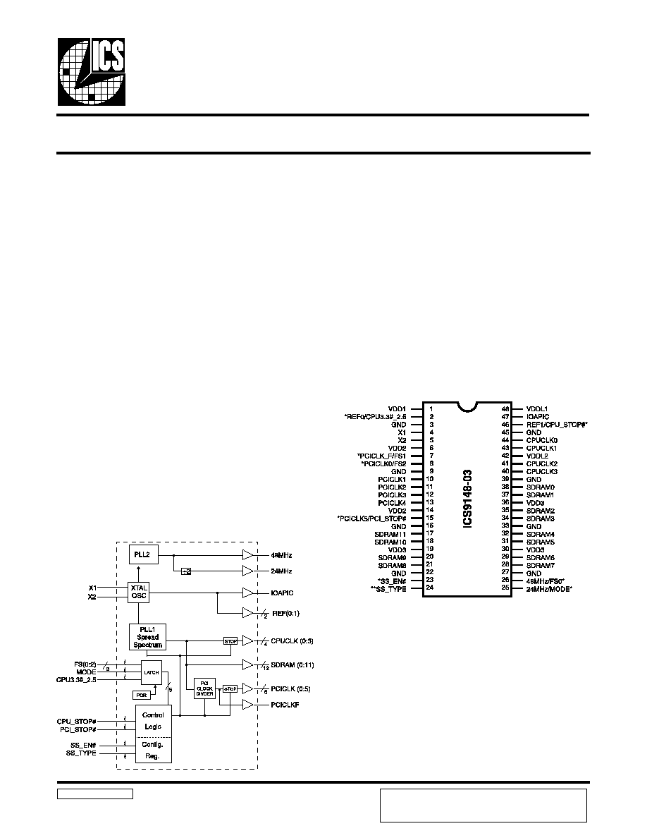
Block Diagram
Pentium is a trademark of Intel Corporation
Frequency Generator & Integrated Buffers for PENTIUM/Pro
TM
9148-03 Rev A 091997P
Pin Configuration
48-Pin SSOP
Power Groups
VDD1 = REF (0:1), XTAL, 24MHz, 48MHz
VDD2 = PCICLK_F, PCICLK(0:5)
VDD3 = SDRAM (0:11), supply for PLL core,
24MHz, 48MHz
VDDL1 = IOAPIC
VDDL2 = CPU (0:3)
* Internal Pull-up Resistor of
240K to 3.3V on indicated inputs
** Internal Pulldown to GND
3.3V outputs: SDRAM, PCI, REF, 48/24MHz.
2.5V or 3.3V outputs: CPU, IOAPIC
20 ohm CPU clock output impedance
20 ohm PCI clock output impedance
Skew from CPU (earlier) to PCI clock - 1 to 4 ns,
center 2.6 ns.
No external load cap for C
L
=18pF crystal
±250 ps CPU, PCI clock skew
400ps (cycle to cycle) CPU jitter
2ms power up clock stable time.
Clock duty cycle 45-55%.
48 pin 300 mil SSOP package
3.3V operation, 5V tolerant input.
The ICS9148-03 generates all clocks required for high
speed RISC or CISC microprocessor systems such as Intel
PentiumPro or Cyrix. Eight different reference frequency
multiplying factors are externally selectable with smooth
frequency transitions.
Features include four CPU, seven PCI and Twelve SDRAM
clocks. Two reference outputs are available equal to the
crystal frequency. Plus the IOAPIC output powered by
VDDL1. One 48 MHz for USB, and one 24 MHz clock for
Super IO. Spread Spectrum built in - ±1.5% modulation to
reduce the EMI. Rise time adjustment for VDD at 3.3V or
2.5V CPU. Additionally, the device meets the Pentium
power-up stabilization, which requires that CPU and PCI
clocks be stable within 2ms after power-up. It is not
recommended to use I/O dual function pin for the slots
(ISA, PCI, CPU, DIMM). The add on card might have a pull up
or pull down.
High drive PCICLK and SDRAM outputs typically provide
greater than 1 V/ns slew rate into 30pF loads. CPUCLK
outputs typically provide better than 1V/ns slew rate into
20pF loads while maintaining 50±5% duty cycle. The REF
and 24 and 48 MHz clock outputs typically provide better
than 0.5V/ns slew rates.
ADVANCE INFORMATION documents contain information on
new products in the sampling or preproduction phase of devel-
opment. Characteristic data and other specifications are subject to
change without notice.
2
ICS9148-03
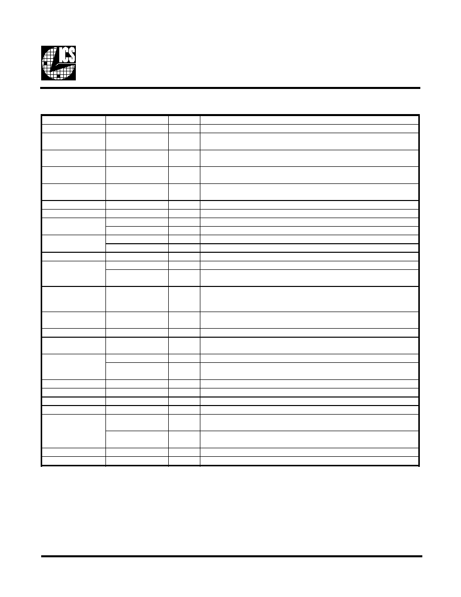
Pin Descriptions
Notes:
1:
Internal Pull-up Resistor of 240K to 3.3V on indicated inputs
2:
Bidirectional input/output pins, input logic levels are latched at internal power-on-reset. Use 10Kohm resistor
to program logic high to VDD logic low to GND.
3. Internal Pulldown Resistor of 240K to GND on SS_type
PIN NUMBER
PIN NAME
TYPE
DESCRIPTION
1
VDD1
PWR
Ref (0:1), XTAL power supply, nominal 3.3V
2
REF0
OUT
14.318 MHz reference clock.
CPU3.3#_2.5
1 ,2
IN
Indicates whether VDDL2 is 3.3V or 2.5V. High=2.5V CPU, LOW=3.3V
CPU. Latched Input.
3,9,16,22,27,
33,39,45
GND
PWR
Ground
4
X1
IN
Crystal input, has internal load cap (33pF) and feedback
resistor from X2
5
X2
OUT
Crystal output, nominally 14.318MHz. Has internal load cap (33pF)
6,14
VDD2
PWR
Supply for PCICLK_F and PCICLK (0:5), nominal 3.3V
7
PCICLK_F
OUT
Free running PCI clock
FS1
1 ,2
IN
Frequency select pin. Latched Input.
8
PCICLK0
OUT
PCI clock output.
FS2
1 ,2
IN
Frequency select pin. Latched Input.
10, 11, 12, 13
PCICLK(1:4)
OUT
PCI clock outputs.
15
PCICLK5
OUT
PCI clock output. (In desktop mode, MODE=1)
PCI_STOP#
1
IN
Halts PCICLK (0:5) clocks at logic 0 level, when input low
(In mobile mode, MODE=0)
17, 18, 20, 21,
28, 29, 31, 32,
34, 35,37,38
SDRAM (0:11)
OUT
SDRAM clock outputs.
19,30,36
VDD3
PWR
Supply for SDRAM (0:11), PLL core and 24, 48MHz clocks, nominal
3.3.V
23
SS_EN#
1
IN
Spread Spectrum Enable. Low =Enable
24
SS_TYPE
3
IN
HIGH = Spread Spectrum down spread. LOW = Spread Spectrum Center
spread. Input has Pulldown to GND
25
24MHz
OUT
24MHz output clock
MODE
1 ,2
IN
Pin 15, pin 46 function select pin, 1=Desktop Mode, 0=Mobile mode.
Latched Input.
26
48MHz
OUT
48MHz output clock
FS0
1 ,2
IN
Frequency select pin. Latched Input.
40, 41, 43, 44
CPUCLK(0:3)
OUT
CPU clock outputs, powered by VDDL2. Low if CPU_STOP#=Low
42
VDDL2
PWR
Supply for CPU (0:3), either 2.5V or 3.3V nominal
46
REF1
OUT
14.318 Mhz reference clock.(in Desktop Mode, MODE=1) This REF Output
is the STRONGER buffer for ISA loads.
CPU_STOP#
1
IN
Halts CPUCLK (0:3) clocks at logic 0 level when input low
(in Mobile Mode, MODE=0)
47
IOAPIC
OUT
IOAPIC clock output. 14.318 MHz Powered by VDDL1.
48
VDDL1
PWR
Supply for IOAPIC, either 2.5V or 3.3V nominal
3
ICS9148-03
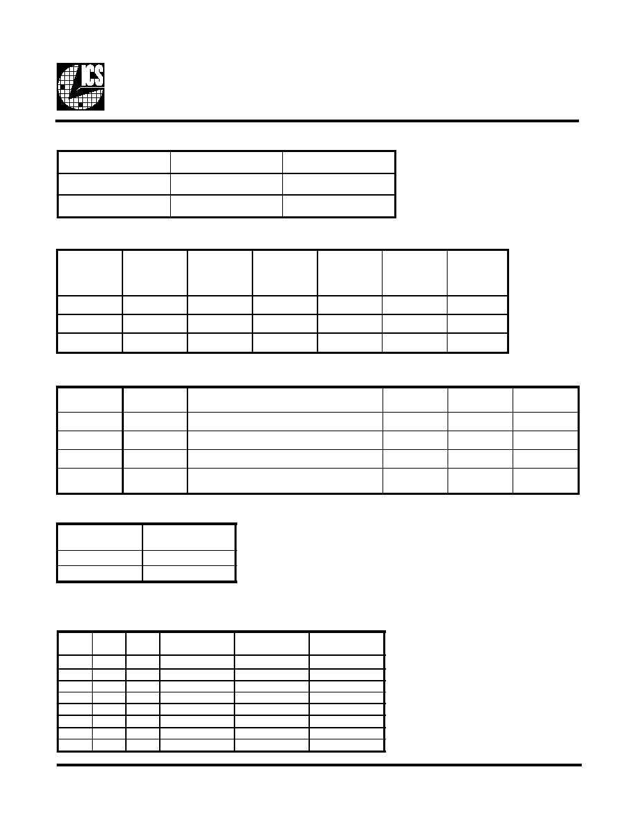
Mode Pin - Power Management Input Control
Power Management Functionality
Spread Spectrum Functionality
CPU3.3#_2.5
Input level
Buffer Selected for
operation at:
1
2.5V VDD
0
3.3V VDD
CPU 3.3#_2.5V Buffer selector for CPUCLK and IOAPIC drivers.
FS2
FS1
FS0
CPU,
SDRAM(M Hz)
PCICLK
(MHz)
REF, IOAPIC
(MHz)
0
0
0
50.0
25.0 (1/2 CPU)
14.318
0
0
1
75.0
32
14.318
0
1
0
83.3
41.65 (1/2 CPU)
14.318
0
1
1
68.5
34.25 (1/2 CPU)
14.318
1
0
0
83.3
33.3
14.318
1
0
1
75.0
37.5 (1/2 CPU)
14.318
1
1
0
60.0
30.0 (1/2 CPU)
14.318
1
1
1
66.8
33.4 (1/2 CPU)
14.318
Functionality
V
DD
1,2,3 = 3.3V±5%, V
DDL
1,2 = 2.5V±5% or 3.3±5%, TA= 0 to 70°C
Crystal (X1, X2) = 14.31818MHz
Pin 23
SSEN#
Pin 24
SS_Type
CPU, SDRAM
and PCICLOCKS
REF, IOAPIC
24MHz
48MHz
0
0
Frequency Modulated Center Spread Mode
14.318MHz
24MHz
48MHz
0
1
Frequency Modulated Down Spread Mode
14.318MHz
24MHz
48MHz
1
0
Normal, Steady Frequency Mode
14.318MHz
24MHz
48MHz
1
1
Not Allowed
(will lower average frequency)
14.318MHz
24MHz
48MHz
MODE, Pin 25
(Latched Input)
Pin 46
Pin 15
0
CPU_STOP#
(INPUT)
PCI_STOP#
(INPUT)
1
REF1
(OUTPUT)
PCICLK5
(OUTPUT)
CPU_STOP#
PCI_STOP#
CPUCLK
Outputs
PCICLK
(0:5)
PCICLK_F,
REF,
24/48MHz
and SDRAM
Crystal
OSC
VCO
0
1
Stopped Low
Running
Running
Running
Running
1
1
Running
Running
Running
Running
Running
1
0
Running
Stopped Low
Running
Running
Running
4
ICS9148-03
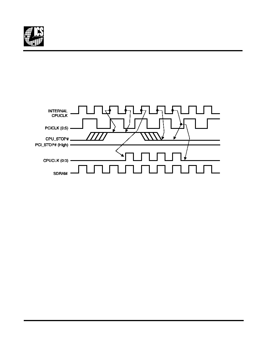
CPU_STOP# Timing Diagram
CPU_STOP# is an asychronous input to the clock synthesizer. It is used to turn off the CPU clocks for low power
operation. CPU_STOP# is synchronized by the ICS9148-03. The minimum that the CPU clock is enabled (CPU_STOP#
high pulse) is 100 CPU clocks. All other clocks will continue to run while the CPU clocks are disabled. The CPU clocks
will always be stopped in a low state and start in such a manner that guarantees the high pulse width is a full pulse. CPU
clock on latency is less than 4 CPU clocks and CPU clock off latency is less than 4 CPU clocks.
Notes:
1. All timing is referenced to the internal CPU clock.
2. CPU_STOP# is an asynchronous input and metastable conditions may exist. This signal
is synchronized to the CPU clocks inside the ICS9148-03.
3. All other clocks continue to run undisturbed.
5
ICS9148-03
Notes:
1. All timing is referenced to the Internal CPUCLK (defined as inside the ICS9148 device.)
2. PCI_STOP# is an asynchronous input, and metastable conditions may exist. This signal is required to be synchronized
inside the ICS9148.
3. All other clocks continue to run undisturbed.
4. CPU_STOP# is shown in a high (true) state.
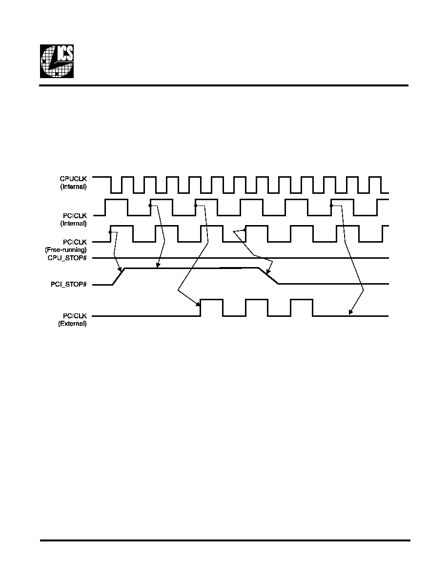
PCI_STOP# Timing Diagram
PCI_STOP# is an asynchronous input to the ICS9148-03. It is used to turn off the PCICLK (0:5) clocks for low power
operation. PCI_STOP# is synchronized by the ICS9148-03 internally. The minimum that the PCICLK (0:5) clocks are
enabled (PCI_STOP# high pulse) is at least 10 PCICLK (0:5) clocks. PCICLK (0:5) clocks are stopped in a low state and
started with a full high pulse width guaranteed. PCICLK (0:5) clock on latency cycles are only one rising PCICLK clock
off latency is one PCICLK clock.