Äîêóìåíòàöèÿ è îïèñàíèÿ www.docs.chipfind.ru
Integrated
Circuit
Systems, Inc.
General Description
Features
ICS9150- 04
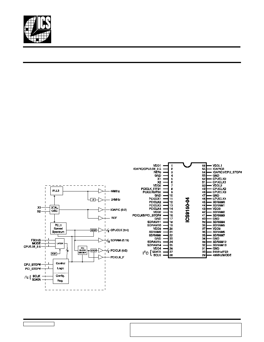
Block Diagram
Pentium is a trademark of Intel Corporation
I
2
C is a trademark of Philips Corporation.
Pentium ProTM and SDRAM Frequency Generator
9150-04 RevD 07/27/98
Pin Configuration
Generates five processor, six bus, one 14.31818MHz
(3.3V) three IOAPIC, 16 SDRAM clocks, 48MHz USB
clock and 24MHz Super I/O clock.
Synchronous clocks skew matched to 250 ps window
on CPUCLKs and 500ps window on PCICLKs
Skew from CPU (earlier) to PCI clock - 1 to 4ns, 2.6ns
nom.
Power Management Control Input pins when MODE
Low
VDD(1:4) - 3.3V ±10%
(inputs 5V tolerant w/series R )
VDDL(1:2) - 2.5V or 3.3V ±5%
I
2
C interface for programming stopclocks plus spread
spectrum options (±0.5% or ±1.5%, center spread or
down spread)
56-pin SSOP package
56-Pin SSOP
The ICS9150-04 generates all clocks required for high speed
RISC or CISC microprocessor systems such as Intel
PentiumPro or Cyrix. Eight different reference frequency
multiplying factors are selectable from 50 to 83.3MHz.
Features include five CPU, seven PCI and Sixteen SDRAM
clocks. One reference output is available equal to the crystal
frequency, plus three IOAPIC outputs powered by VDDL1.
One 48 MHz for USB is provided plus a 24 MHz. Spread
Spectrum built in up to ±1.5% modulation to reduce EMI.
Serial programming I
2
C interface allows changing functions,
stop clock programing and Frequency selection. Rise time
adjustment for VDD at 3.3V or 2.5V CPU. Additionally, the
device meets the Pentium power-up stabilization, which
requires that CPU and PCI clocks be stable within 2ms after
power-up.
High drive PCICLK and SDRAM outputs typically provide
greater than 1 V/ns slew rate into 30pF loads. CPUCLK outputs
typically provide better than 1V/ns slew rate into 20pF loads
while maintaining 50±5% duty cycle. The REF 24 and 48 MHz
and SDRAM 12, 13 clock outputs typically provide better
than 0.5V/ns slew rates.
Power Groups
VDD1 = REF, X1, X2
VDD2 = PCICLK_F, PCICLK(0:5)
VDD3 = SDRAM (0:15), supply for PLL core,
VDD4 = 48MHz, 24MHz
VDDL1 = IOAPIC (0:2)
VDDL2 = CPUCLK (0:4)
ICS reserves the right to make changes in the device data identified in this
publication without further notice. ICS advises its customers to obtain the latest
version of all device data to verify that any information being relied upon by the
customer is current and accurate.
2
ICS9150- 04
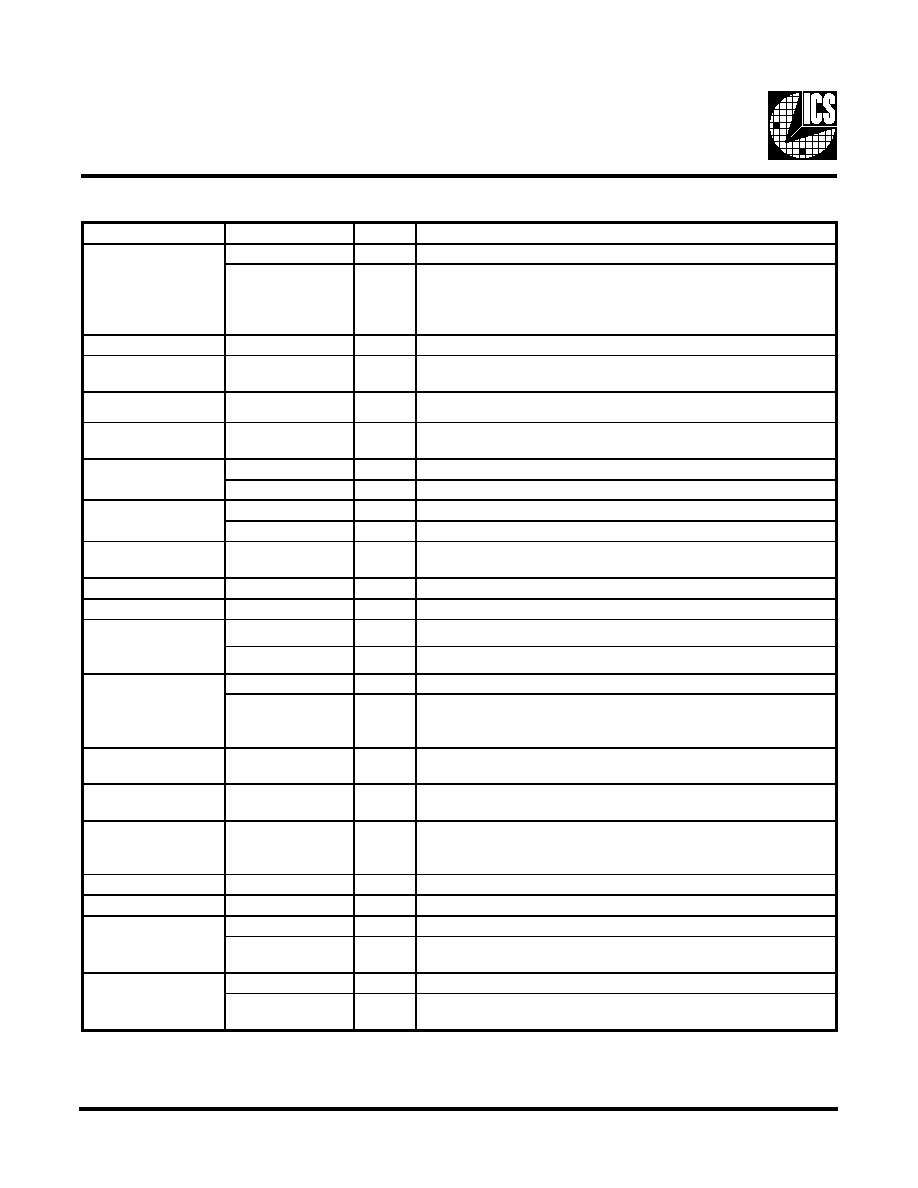
Pin Descriptions
PIN NUMBER
PIN NAME
TYPE
DESCRIPTION
2
IOAPIC2
OUT
IOAPIC clock output (14.318MHz) powered by VDDL1
CPU3.3#_2.5
IN
Indicates whether VDDL1 & VDDL2 are 3.3 or 2.5V. Output
buffer strength compensates for VDDL selection to maintain
CPU to SDRAM skew. High = 2.5V, Low = 3.3V. Has pull-up
to VDDL1, must use series resistor for 3.3 or 5V logic levels.
3
REF0
OUT
14.318 MHz reference clock outputs.
4, 10, 17, 23, 31, 34,
40, 47, 53
GND
PWR
Ground.
5
X1
IN
14.318MHz input. Has internal load cap, (nominal 33pF).
6
X2
OUT
Crystal output. Has internal load cap (33pF) and feedback
resistor to X1
8
PCICLK_F
OUT
Free running BUS clock during PCI_STOP#=0.
FS1
1
IN
Latched frequency select input. Has pull-up to VDD2.
9
PCICLK0
OUT
BUS clock output
FS2
1
IN
Latched frequency select input. Has pull-up to VDD2.
11, 12,
13, 14
PCICLK (1:4)
OUT
BUS clock outputs.
27
SDATA
IN
Serial data in for serial config port. (I
2
C)
28
SCLK
IN
Clock input for serial config port. (I
2
C)
30
24MHz
OUT
24MHz clock output for Super I/O or FD.
FS0
1
IN
Latched frequency select input. Has pull-up to VDD4.
29
48MHz
OUT
48MHz clock output for USB.
MODE
1
IN
Latched input for MODE select. Converts 2 outputs to power
management CPU_STOP# and PCI_STOP# when low. Has pull-
up to VDD4.
1, 7, 15, 20, 26, 37,
43
VDD2, VDD1,
VDD3, VDD4
PWR
Nominal 3.3V power supply, see power groups for function.
50, 56
VDDL2, VDDL1
PWR
CPU and IOAPIC clock buffer power supply, either 2.5 or 3.3V
nominal.
18, 19, 21, 22, 24,
25, 32, 33, 35, 36,
38, 39, 41, 42, 44, 45
SDRAM (0:15)
OUT
SDRAM clocks
55
IOAPIC0
OUT
IOAPIC clock output. (14.318 MHz) Poweredby VDDL1
46, 48, 49, 51, 52
CPUCLK (0:4)
OUT
CPU Output clocks. Powered by VDDL2 (60 or 66.6MHz)
54
IOAPIC1
OUT
IOAPIC clock output. (14.31818 MHz) Powered by VDDL1
CPU_STOP#
IN
Halts CPUCLK clocks at logic "0" level when low. (in mobile,
MODE=0)
16
PCICLK5
OUT
PCI BUS clock 5
PCI_STOP#
IN
Halts PCICLK (0:4) at logic "0" level when low. (in mobile,
MODE=0)
Notes:
1:
Bidirectional input/output pins, input logic levels are latched at internal power-on-reset. Use 10Kohm resistor
to program logic Hi to VDD or GND for logic low.
3
ICS9150-04
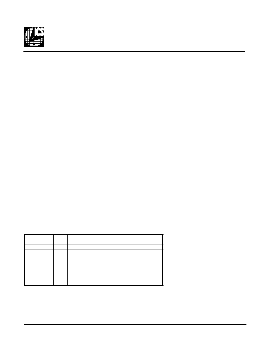
Definitions
5 Latched Inputs at Internal Power-On Reset:
MODE................................ 48MHz/MODE
CPU 3.3_2.5#V .................. IOAPIC2/CPU3.3#_2.5
FS0 ..................................... 24MHz/FS0
FS1 ..................................... PCICLK_F/FS1
FS2 ..................................... PCICLK0/FS2
Pin shared as
2 Realtime Inputs
Pins 27, 28 - I
2
C Serial input SDATA & SCLK
Pull-ups
2 pins with input latch or I/O have IOAPIC output function with VDDL1 which can be at 2.5V or 3.3V. These inputs will
have to use series resistor (above 100
)
to external VIN to be 3.3 & 5V logic input tolerant.
PMOS output stage provides input clamp diode to VDDL.
Nwell resistor Pull-ups 100 to 150K
to local VDD
(ie on IOAPIC pins use VDDL1, on FS1, 2 use VDD2, FS0=VDD4 and PCI_STOP#)
Functionality
V
DD
1,2,3 = 3.3V±5%, V
DDL
1,2 = 2.5V±5% or 3.3±5%, TA=0 to 70°C
Crystal (X1, X2) = 14.31818MHz
FS2
FS1
FS0
CPU,
SDRAM(MHz)
PCICLK (MHz)
REF, IOAPIC
(MHz)
1
1
1
66.8
33.4 (1/2 CPU)
14.318
1
1
0
60.0
30.0 (1/2 CPU)
14.318
1
0
1
75.0
37.5 (1/2 CPU)
14.318
1
0
0
83.3
33.3
14.318
0
1
1
68.5
34.25 (1/2 CPU)
14.318
0
1
0
83.3
41.65 (1/2 CPU)
14.318
0
0
1
75.0
32
14.318
0
0
0
50.0
25.0 (1/2 CPU)
14.318
4
ICS9150- 04
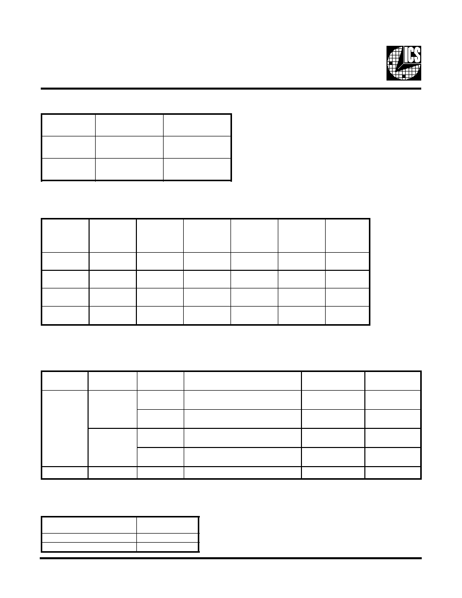
Mode Pin - Power Management Input Control
Power Management Functionality
Spread Spectrum Functionality
CPU 3.3#_2.5V Buffer selector for CPUCLK driver.
CPU3.3#_2.5
Latched Input Level
Buffer Selected
for Operation at:
1
2.5V VDD
0
3.3V VDD
BYTE0, Bit1
SS_EN
BYTE0, Bit2
SS_TYPE
BYTE0, Bit7
CPU, SDRAM
and PCI CLOCKS
REF, IOAPIC
24,48MHz
1
0
0
Frequency modulated in center spread
spectrum mode +1.5%, -1.5%
14.318MHz
24,48MHz
1
Frequency modulated in center spread
spectrum mode +0.5%, -0.5%
14.318MHz
24,48MHz
1
0
Frequency modulated in down spread
spectrum mode +0%, -3.0%
14.318MHz
24,48MHz
1
Frequency modulated in down spread
spectrum mode +0%, -1.0%
14.318MHz
24,48MHz
0
X
X
Normal, Steady frequency mode
14.318MHz
24,48MHz
MODE, Pin 55
Pin 54
Pin 16
0
CPU_STOP#
Input
PCI_STOP#
Input
1
IOAPIC1
Output
PCICLK5
Output
CPU_STOP#
PCI_STOP#
CPUCLK
Outputs
PCICLK(0:5)
Outputs
PCICLK_F,
REF, IOAPIC
48MHz
and SDRAM
Crystal
OSC
VCO
0
0
Stopped Low
Stopped Low
Running
Running
Running
0
1
Stopped Low
Running
Running
Running
Running
1
0
Running
Stopped Low
Running
Running
Running
1
1
Running
Running
Running
Running
Running

5
ICS9150-04
VDD(1,2,3,4)
This is the power supply to the internal core logic of the
device as well as the clock output buffers for REF, PCICLK,
and SDRAM.
This pin operates at 3.3V volts. Clocks from the listed buffers
that it supplies will have a voltage swing from Ground to this
level. For the actual guaranteed high and low voltage levels
for the Clocks, please consult the DC parameter table in this
data sheet.
VDDL1,2
This is the power supply for the CPUCLK and IOAPIC output
buffers. The voltage level for these outputs may be 2.5 or
3.3volts. Clocks from the buffers that each supplies will have
a voltage swing from Ground to this level. For the actual
Guaranteed high and low voltage levels of these Clocks,
please consult the DC parameter table in this Data Sheet.
GND
This is the power supply ground (common or negative) return
pin for the internal core logic and all the output buffers.
X1
This input pin serves one of two functions. When the device
is used with a Crystal, X1 acts as the input pin for the
reference signal that comes from the discrete crystal. When
the device is driven by an external clock signal, X1 is the
device input pin for that reference clock. This pin also
implements an internal Crystal loading capacitor that is
connected to ground. With nominal value of 33pF no external
load cap is needed for a CL=17 to 18pF crystal.
X2
This Output pin is used only when the device uses a Crystal
as the reference frequency source. In this mode of operation,
X2 is an output signal that drives (or excites) the discrete
Crystal. The X2 pin will also implement an internal Crystal
loading capacitor that is nominally 33pF.
CPUCLK (0:4)
These Output pins are the Clock Outputs that drive processor
and other CPU related circuitry that requires clocks which are
in tight skew tolerance with the CPU clock. The voltage
swing of these Clocks is controlled by the Voltage level
applied to the VDDL2 pin of the device. See the Functionality
Table for a list of the specific frequencies that are available
for these Clocks and the selection codes to produce them.
SDRAM(0:15)
These Output Clocks are used to drive Dynamic RAMs and
are low skew copies of the CPU Clocks. The voltage swing of
the SDRAMs output is controlled by the supply voltage
that is applied to VDD3 of the device. Operates at 3.3 volts.
IOAPIC (0:2)
These Outputs are fixed frequency Output Clocks that run at
the Reference Input frequency (typically 14.31818MHz) . Its
voltage level swing is controlled by VDDL1 and may operate
at 2.5 or 3.3volts.
REF0
The REF Output is a fixed frequency Clock that runs at the
same frequency as the Input Reference Clock X1 or the
Crystal (typically 14.31818MHz) attached across X1 and X2.
Technical Pin Function Descriptions
PCICLK_F
This Output is equal to PCICLK(0:5). It is FREE RUNNING, and
will not be stopped by PCI_STOP#.
PCICLK (0:5)
These Output Clocks generate all the PCI timing requirements
for a Pentium/Pro based system. They conform to the current
PCI specification. They run at 1/2 CPU frequency, for most
choices of FS (0:2).
FS(0:2)
These Input pins control the frequency of the Clocks at the
CPU, PCICLK and SDRAM output pins. These inputs are
Bidirectional Input/Output pins, latched at internal power-on-
reset.
MODE
This Input pin is used to select the Input function of the I/O
pins. An active Low will place the I/O pins in the Input mode
and enable the stop clock functions. (This is the Power
Management Mode)
CPU_STOP#
This is a synchronous active Low Input pin used to stop the
CPUCLK clocks in an active low state. All other Clocks including
SDRAM clocks will continue to run while this function is
enabled. The CPUCLKs will have a turn ON latency of at least
3 CPU clocks. This input pin valid only when MODE=0 (Power
Management Mode)
PCI_STOP#
This is a synchronous active Low Input pin used to stop the
PCICLK clocks in an active low state. It will not effect PCICLK_F
nor any other outputs. This input pin valid only when MODE=0
(Power Management Mode)
I
2
C (SDATA, SCLK)
The SDATA and SCLOCK Inputs are use to program the device.
The clock generator is a slave-receiver device in the I
2
C
protocol. It will allow read-back of the registers. See
configuration map for register functions. The I
2
C specification
in Philips I
2
C Peripherals Data Handbook (1996) should be
followed.
48MHz
This is a fixed frequency Clock output at 48MHz that is typically
used to drive USB devices.
24MHz
This pin is a fixed frequency clock output typically used to
drive Super I/O devices.
CPU 3.3#_2.5
This Input pin controls the CPU output buffer strength for
skew matching CPU and SDRAM outputs to compensate for
the external VDDL supply condition. It is important to use this
function when selecting power supply requirements for
VDDL1,2. A logic 1 (ground) will indicate 2.5V operation and
a logic 0 will indicate 3.3V operation. This pin has an internal
pullup resistor to VDD.