Äîêóìåíòàöèÿ è îïèñàíèÿ www.docs.chipfind.ru
Integrated
Circuit
Systems, Inc.
General Description
Features
ICS9159-06
Frequency Generator and Buffer for Pentium Systems
9159-06 Rev C 091897
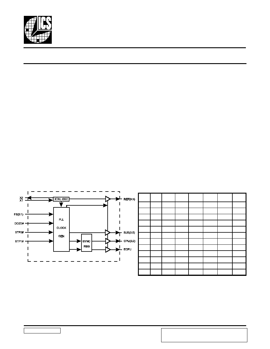
Block Diagram
The ICS9159-06 is a low cost frequency generator designed
specifically for Pentium systems. The integrated buffer minimizes
skew and provides the early CPU clock required by some
chipsets such as the OPTi VIPER. A 14.318 MHz XTAL oscillator
provides the reference clock to generate standard Pentium
frequencies. The CPU clock makes gradual frequency transitions
without violating the PLL timing of internal microprocessor
clock multipliers.
Asynchronous 33.3 MHz PCI bus operation is supported,
in-dependent of the CPU operating frequency. Green PC
systems are supported through power-down, doze, and
glitch-free stop clock modes.
Four CPU clocks operate up to 66 MHz at 3.3V with
glitch-free start and stop plus smooth transitions
3-6ns early CPU clock supports OPTi VIPER systems
Selection of 8 frequencies, tristate, or power-down
Six BUS clocks support asynchronous PCI bus
operation
±250ps skew between synchronous outputs
Integrated buffer outputs drive up to 30pF loads
3.1V -5.5V supply range
28-pin 300-mil SOIC package
COMPAQ is a trademark of Compaq Computers.
Pentium is a trademark of Intel Corporation.
Applications
Ideal for green Pentium and 486 PCI systems
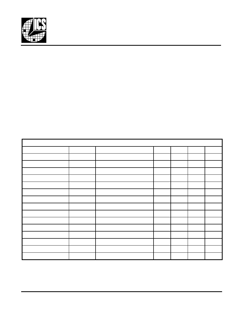
Functionality
3.1 to 5.5V, 0-70° Crystal=14.318 MHz input
STP0# STP1# DOZE#
FS(0:1)
CPU(0:1)
(MHz)
CPU2,
ECPU
BUS(0:5)
(MHz)
REF(0:3)
(MHz)
1
X
1
00
66.6*
66.6*
33.3
14.318
1
X
1
01
60*
60*
33.3
14.318
1
X
1
10
50
50
33.3
14.318
1
X
1
11
40
40
33.3
14.318
1
X
0
00
33.3
33.3
16.7
14.318
1
X
0
01
30
30
16.7
14.318
1
X
0
10
25
25
16.7
14.318
1
X
0
11
22.5
22.5
16.7
14.318
0
1
1
- -
Stop
Run
Run
14.318
0
0
1
X X
Stop
Stop
Stop
14.318
0
0*
0*
X X
Low
Low
Low
14.318
0
1
0
X X
Tristate Tristate Tristate 14.318
* 3.3 volt operation only. ** 000 mode powers-down the
PLL sections and forces the outputs low. To ensure glitch-
free start and stop of the CPU and BUS clocks enter 000
from 001 and exit 000 through 001.
PRODUCT PREVIEW documents contain information on new
products in the sampling or preproduction phase of development.
Characteristic data and other specifications are subject to change
without notice.
Preliminary Product Preview
2
ICS9159-06
Preliminary Product Preview
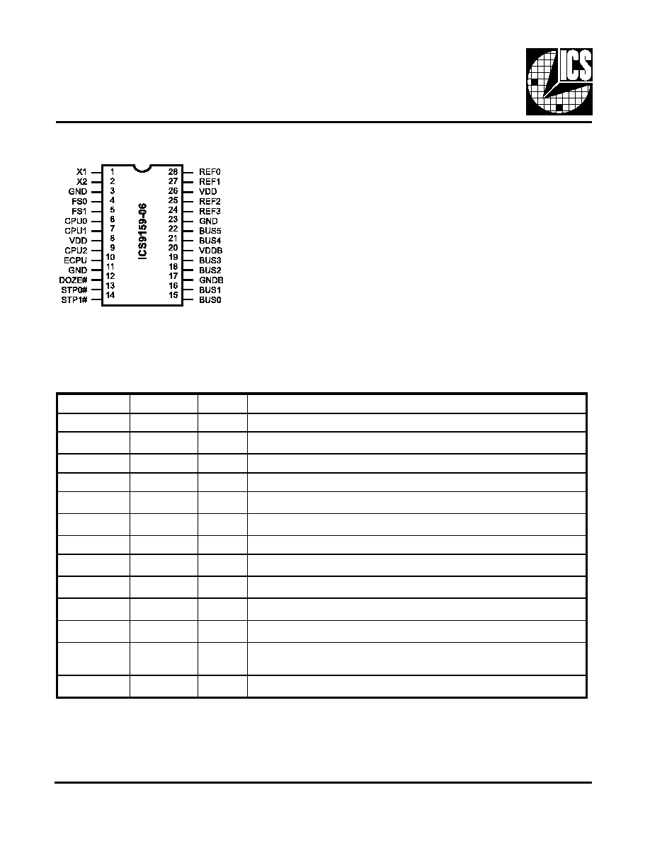
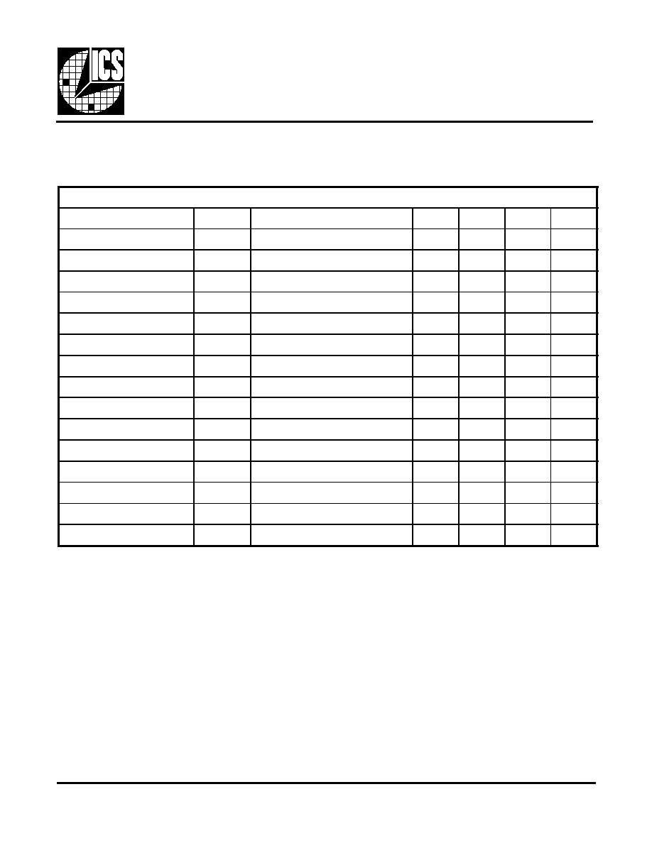
Pin Descriptions
28-Pin 300-mil SOIC
Pin Configuration
PIN NUMBER
PIN NAME
TYPE
DESCRIPTION
8, 26
VDD
PWR
Power for logic, CPU and fixed frequency output buffers.
1
X1
IN
XTAL or external reference frequency input. This input includes XTAL load
capacitance and feedback bias for a 0.5 - 20 MHz XTAL.**
2
X2
OUT
XTAL output which includes XTAL load capacitance.**
3, 11, 23
GND
PWR
Ground for logic, CPU and fixed frequency output buffers.
6, 7, 9
CPU(0:2)
OUT
Processor clock outputs which are a multiple of the input reference frequency as
shown in the table.
4, 5
FS(0:1)
IN
Frequency multiplier select pins. See table. These inputs have internal pull-up
devices.
20
VDDB
PWR
Power for BUS output buffers.
15, 16, 18 19,
21, 22
BUS(0:5)
OUT
Bus clock outputs are fixed at 33.3 or 16.7 MHz.*
24, 25, 27, 28
REF(0:3)
OUT
REF is a buffered copy of the crystal oscillator or reference input clock,
nominally 14.31818 MHz.*
10
ECPU
OUT
Early processor clock output which is the same frequency as CPU(0:2). This clock
leads CPU(0:2) by 3-6nS.
12
DOZE#
IN
Reduces CPU, ECPU and BUS clock outputs as shown in the functionality table
when at a logic low level.
13, 14
STP0#, STP1#
IN
Synchronously stops the CPU, ECPU and BUS clocks per the description in the
functionality table. Can also be used to tristate all outputs when the DOZE pin is
low.
17
GNDB
PWR
This ground return path is brought on separately to permit separating the noise
impulses from high output buffers from affecting sensitive internal circuitry.***
*
Assuming 14.31818 MHz input clock or crystal.
** Device provides 18pF load for crystal load capacitance at each pin.
*** Ground for bus clock buffers.
3
ICS9159-06
Preliminary Product Preview
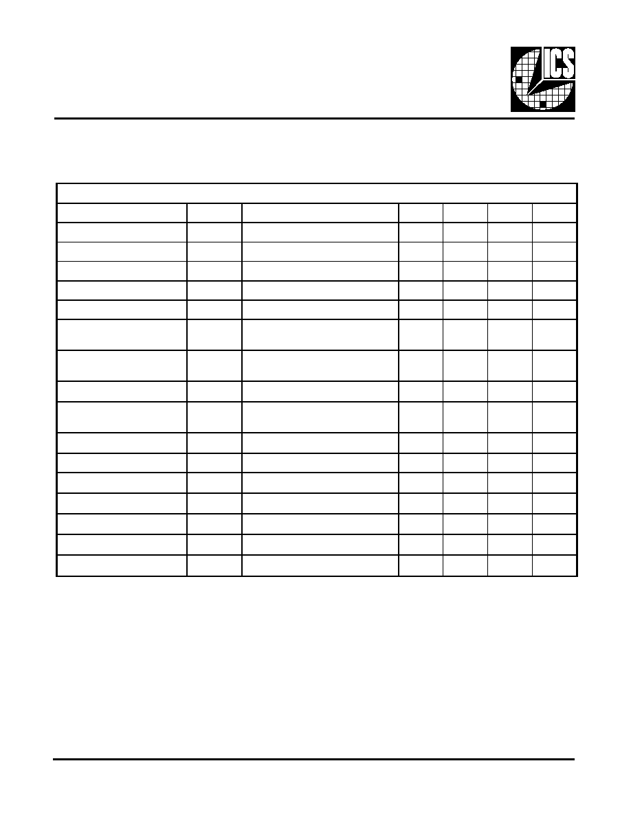
Absolute Maximum Ratings
Electrical Characteristics at 3.3V
Supply Voltage .......................................................................................................... 7.0 V
Logic Inputs ....................................................................... GND 0.5 V to V
DD
+0.5 V
Ambient Operating Temperature ............................................................. 0°C to +70°C
Storage Temperature ........................................................................... 65°C to +150°C
V
DD
= 3.0 3.7 V, T
A
= 0 70
°
C unless otherwise stated
Note 1: Parameter is guaranteed by design and characterization. Not 100% tested in production.
Stresses above those listed under Absolute Maximum Ratings may cause permanent damage to the device. These ratings
are stress specifications only and functional operation of the device at these or any other conditions above those listed
in the operational sections of the specifications is not implied. Exposure to absolute maximum rating conditions for
extended periods may affect product reliability.
DC Characteristics
PARAMETER
SYMBOL
TEST CONDITIONS
MIN
TYP
MAX
UNITS
Input Low Voltage
V
IL
-
-
0.2V
DD
V
Input High Voltage
V
IH
0.7V
DD
-
-
V
Input Low Current
I
IL
V
IN
=0V
-28.0
-10.5
-
µA
Input High Current
I
IH
V
IN
=V
DD
-5.0
-
5.0
µA
Output Low Current
1
I
OL
V
OL
=0.8V; for CPU & BUS
30.0
47.0
-
mA
Output High Current
1
I
OH
V
OL
=2.0V; for CPU & BUS
-
-66.0
-42.0
mA
Output Low Current
1
I
OL
V
OL
=0.8V; for REF
25.0
38.0
-
mA
Output High Current
1
I
OH
V
OL
=2.0V; for REF
-
-47.0
-30.0
mA
Output Low Voltage
V
OL
I
OL
=15mA; for CPU & BUS
-
0.30
.4
V
Output High Voltage
1
V
OH
I
OH
=-30mA; for CPU & BUS
2.4
2.8
-
V
Output Low Voltage
V
OL
I
OL
=12.5mA; for REF
-
0.30
.4
V
Output High Voltage
1
V
OH
I
OH
=-20mA; for REF
2.4
2.8
-
V
Supply Current
I
DD
@66.66 MHz; all outputs unloaded
-
55
110
mA
Supply Current, Power-down
I
DD
(PD)
@000 Mode (Power-down)
-
8
20
mA
Supply Current, Stop Mode
I
DD
(STOP)
@001 Mode (Stop Mode)
-
35
70
mA
4
ICS9159-06
Preliminary Product Preview
Electrical Characteristics at 3.3V
V
DD
= 3.1 3.7 V, T
A
= 0 70
°
C
Note 1: Parameter is guaranteed by design and characterization. Not 100% tested in production.
AC Characteristics
PARAMETER
SYMBOL
TEST CONDITIONS
MIN
TYP
MAX
UNITS
Rise Time
1
T
r1
20pF load, 0.8 to 2.0V, CPU & BUS
-
0.9
1.5
ns
Fall Time
1
T
f1
20pF load, 2.0 to 0.8V, CPU & BUS
-
0.8
1.4
ns
Rise Time
1
T
r2
20pF load, 20% to 80%, CPU & BUS
-
1.5
2.5
ns
Fall Time
1
T
f2
20pF load, 80% to 20%, CPU & BUS
-
1.4
2.4
ns
Duty Cycle
1
D
t
20pF load; @VOUT=1.4V
40
50
60
%
Jitter, One Sigma
1
T
j1s
CPU; ECPU
Load=20pF;
FOUT >25 MHz
-
60
150
ps
Jitter, Absolute
1
T
jab
CPU; ECPU
Load=20pF,
FOUT >25 MHz
-350
-
350
ps
Jitter, One Sigma
1
T
j1s
BUS(0:2); REF(0:3); CPU
25 MHz;
Load=20pF; Comp. to the period
-
0.7
2.0
%
Jitter, Absolute
1
T
jab
BUS(0:2); REF(0:3); CPU
25 MHz;
Load=20pF;
Comp. to the period
-3.0
-
3.0
%
Input Frequency
1
F
i
0.5 14.318 20 MHz Logic Input
Capacitance 1 CIN Logic input pins
-
5
-
pF
Crystal Oscillator Capacitance
1
CINX
X1, X2 pins
-
18
-
pF
Power-on Time
1
t
on
From V
DD
=1.6V to 1 st crossing of
66.6 MHz V
DD
supply ramp < 40ms
-
2.5
4.5
ms
Frequency Settling Time
1
t
s
From 1 st crossing of acquisition to
<1% settling
-
2.0
4.0
ms
Clock Skew Window
1
T
sk1
CPU to CPU;
Load=20pF; @1.4V
-
150
250
ps
Clock Skew Window
1
T
sk2
BUS to BUS and REF to REF;
Load=20pF; @1.4V
-
300
500
ps
Clock Skew Window
1
T
sk3
ECPU to CPU(0:2);
Load=20pF; @1.4V
3.0
5.0
6.0
ns
5
ICS9159-06
Preliminary Product Preview
Electrical Characteristics at 5.5V
V
DD
= 4.5 5.5 V, T
A
= 0 70
°
C
Note 1: Parameter is guaranteed by design and characterization. Not 100% tested in production.
DC Characteristics
PARAMETER
SYMBOL
TEST CONDITIONS
MIN
TYP
MAX
UNITS
Input Low Voltage
V
IL
-
-
0.2V
DD
V
Input High Voltage
V
IH
0.7V
DD
-
-
V
Input Low Current
I
IL
V
IN
= 0V
-40.0
16.0
-
µA
Input High Current
I
IH
V
IN
= V
DD
-5.0
-
5.0
µA
Output Low Current
1
I
OL
V
OL
= 0.8V; for CPU & BUS
40.0
62.0
-
mA
Output High Current
1
I
OH
V
OL
= 2.0V; for CPU & BUS
-
-140.0
-90.0
mA
Output Low Current
1
I
OL
V
OL
= 0.8V; for REF
30.0
50.0
-
mA
Output High Current
1
I
OH
V
OL
= 2.0V; for REF
-
-100.0
-60.0
mA
Output Low Voltage
V
OL
I
OL
= 20mA; for CPU & BUS
-
0.3
0.4
V
Output High Voltage
1
V
OH
I
OH
= -70mA; for CPU & BUS
2.4
2.8
-
V
Output Low Voltage
V
OL
I
OL
= 15mA; for REF
-
0.30
.4
V
Output High Voltage
1
V
OH
I
OH
=-50mA; for REF
2.4
2.8
-
V
Supply Current
I
DD
@50.0 MHz; all outputs unloaded
-
95.0
200.0
mA
Supply Current, Power-down
I
DD
(PD)
@000 Mode (Power-down)
-
16.0
40.0
mA
Supply Current, Stop Mode
I
DD
(STOP)
@001 Mode (Stop Mode)
-
70.0
140.0
mA