Integrated
Circuit
Systems, Inc.
General Description
Features
ICS9169C-26
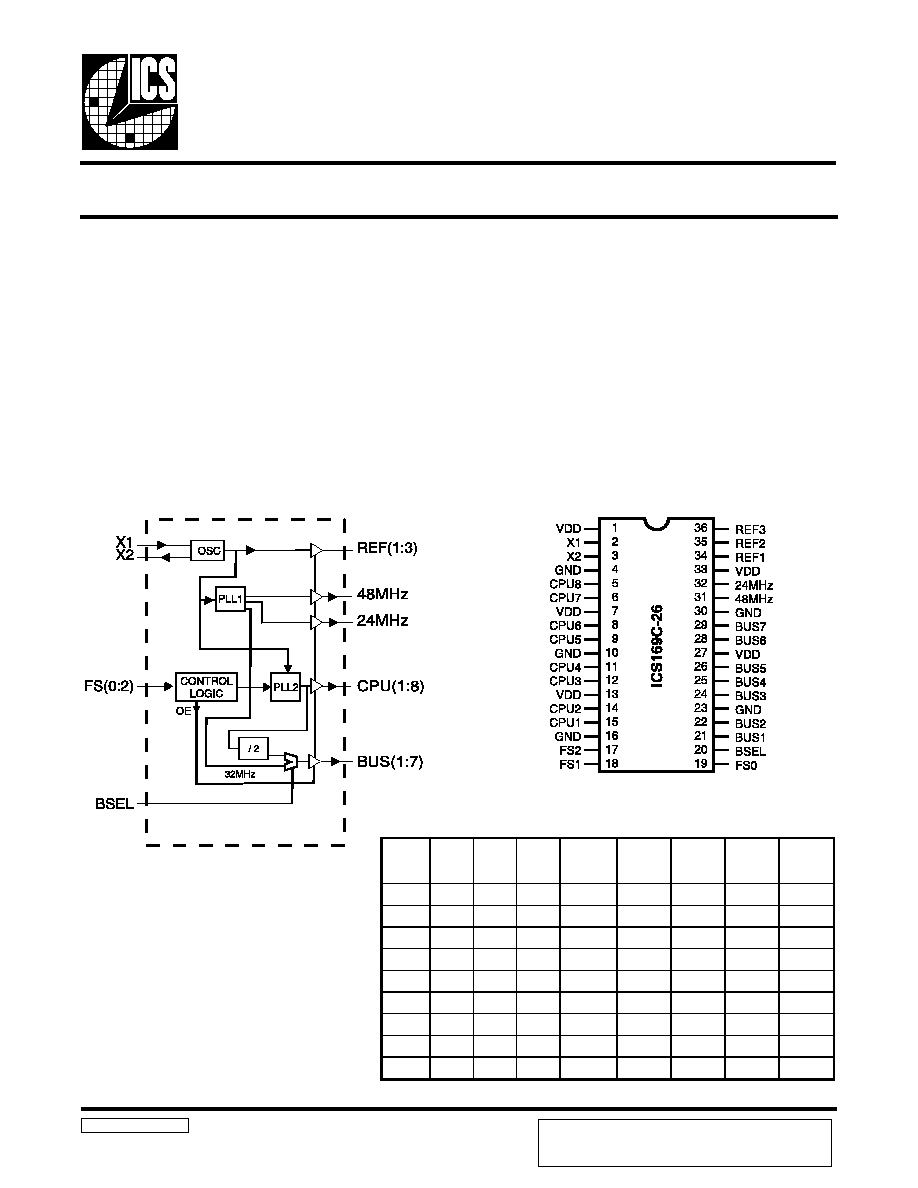
Block Diagram
Frequency Generator and Integrated Buffers
9169C-26RevB091997P
Pin Configuration
Twelve selectable CPU clocks operate up to 83.3 MHZ
Eight selectable CPU clocks operate up to100 MHz
Maximum CPU jitter of ±200ps
Seven BUS clocks support sync or async bus operation
500ps skew window for all synchronous clock edges
CPU clocks to BUS clocks in sync mode skew
1-4ns (CPU early)
Integrated buffer outputs drive up to 30pF loads
3.0V - 3.7V supply range
36-pin SSOP package
48 MHz clock for USB support and 24 MHz clock for FD
36-Pin SSOP
Functionality
3.3V±10%, 0-70
∞
C
Crystal (X1, X2) = 14.31818 MHz
Pentium is a trademark on Intel Corporation.
The ICS9169C-26 is a low-cost frequency generator
designe specifically for Pentium-based chip set systems.
The integrated buffer minimizes skew and provides all the
clocks required. A 14.318 MHz XTAL oscillator provides
the reference clock to generate standard Pentium
frequencies. The CPU clock makes gradual frequency
transitions without violating the PLL timing of internal
microprocessor clock multipliers.
Either synchronous (CPU/2) or asynchronous (32 MHz)
PCI bus operation can be selected.
BSEL
FS2
FS1
FS0
CPU
(1:8)
MHz
BUS
(0:7)
MHz
48 MHz 24 MHz
REF
(1:3)
0
0
0
0
55
27.5
48
24
14.318
0
0
0
1
80
40
48
24
14.318
0
0
1
0
100
50
48
24
14.318
0
0
1
1
75
37.5
48
24
14.318
0
1
0
0
50
25
48
24
14.318
0
1
0
1
66.6
33.3
48
24
14.318
0
1
1
0
60
30.0
48
24
14.318
0
1
1
1
Tristate Tristate Tristate Tristate Tristate
1
select select select Tristate
32.0
48
24
14.318
PRODUCT PREVIEW documents contain information on new
products in the sampling or preproduction phase of development.
Characteristic data and other specifications are subject to change
without notice.
Preliminary Product Preview

2
ICS169C-26
Preliminary Product Preview
Pin Descriptions
PIN NUMBER
PIN NAME
TYPE
DESCRIPTION
1, 7, 13, 27, 33
VDD
PWR
Power for control logic, PLL and output buffers.
2
X1
IN
XTAL or external reference frequency input. This input
includes XTAL load capacitance and feedback bias for a 12 -
16 MHz crystal, nominally 14.31818 Mhz.
3
X2
OUT
XTAL output which includes XTAL load capacitance.
4, 10, 16, 23, 30
GND
PWR
Ground for logic, PLL and output buffers.
5, 6, 8, 9, 11, 12, 14, 15
CPU(1:8)
OUT
Processor clock outputs which are a multiple of the input
reference frequency as shown in the table above.
17, 18, 19
FS(1:2)
IN
Frequency multiplier select pins. See table above. These inputs
have internal pull-up devices.
20
BSEL
IN
Selector for synchronous or asynchronous bus operation.
21, 22, 24, 25, 26, 28, 29
BUS(1:7)
OUT
Bus clock outputs.
31
48MHz
OUT
Fixed 48 MHz clock (with 14.318 MHz input).
32
24MHz
OUT
Fixed 24 MHz clock (with 14.318 MHz input).
34, 35, 36
REF(1:3)
OUT
REF is a buffered copy of the crystal oscillator or reference
input clock, nominally 14.31818 Mhz.
3
ICS169C-26
Preliminary Product Preview
Absolute Maximum Ratings
Electrical Characteristics at 3.3V
Supply Voltage . . . . . . . . . . . . . . . . . . . . . . . . . . 7.0 V
Logic Inputs . . . . . . . . . . . . . . . . . . . . . . . . . . . . GND 0.5 V to V
DD
+0.5 V
Ambient Operating Temperature . . . . . . . . . . . . 0∞C to +70∞C
Storage Temperature . . . . . . . . . . . . . . . . . . . . . . 65∞C to +150∞C
V
DD
= 3.0 3.7 V, T
A
= 0 70
∞
C unless otherwise stated
Note 1: Parameter is guaranteed by design and characterization. Not 100% tested in production.
Stresses above those listed under Absolute Maximum Ratings may cause permanent damage to the device. These ratings are
stress specifications only and functional operation of the device at these or any other conditions above those listed in the
operational sections of the specifications is not implied. Exposure to absolute maximum rating conditions for extended
periods may affect product reliability.
DC Characteristics
PARAMETER
SYMBOL
TEST CONDITIONS
MIN
TYP
MAX
UNITS
Input Low Voltage
V
IL
-
-
0.2V
DD
V
Input High Voltage
V
IH
0.7V
DD
-
-
V
Input Low Current
I
IL
V
IN
=0V
-28.0
-10.5
-
µ A
Input High Current
I
IH
V
IN
=V
DD
-5.0
-
5.0
µ A
Output Low Current1
I
OL
V
OL
=0.8V; for CPUs & BUSes
30.0
47.0
-
mA
Output High Current1
I
OH
V
OL
=2.0V; for CPUs & BUSes
-
-66.0
-42.0
mA
Output Low Current1
I
OL
V
OL
=0.8V; for fixed CLKs
25.0
38.0
-
mA
Output High Current1
I
OH
V
OL
=2.0V; for fixed CLKs
-
-47.0
-30.0
mA
Output Low Voltage1
V
OL
I
OL
=15mA; for CPUs & BUSes
-
0.3
0.4
V
Output High Voltage1
V
OH
I
OH
=-30mA; for CPUs & BUSes
2.4
2.8
-
V
Output Low Voltage1
V
OL
I
OL
=12.5mA; for fixed CLKs
-
0.3
0.4
V
Output High Voltage1
V
OH
I
OH
=-20mA; for fixed CLKs
2.4
2.8
-
V
Supply Current
I
DD
@66.6 MHz; all outputs unloaded
-
55
110
mA
4
ICS169C-26
Preliminary Product Preview
Electrical Characteristics at 3.3V
V
DD
= 3.0 3.7 V, T
A
= 0 70
∞
C unless otherwise stated
Note 1: Parameter is guaranteed by design and characterization. Not 100% tested in production.
AC Characteristics
PARAMETER
SYMBOL
TEST CONDITIONS
MIN
TYP
MAX
UNITS
Rise Time
1
T
r1
20pF load, 0.8 to 2.0V
CPU & BUS
-
0.9
1.5
ns
Fall Time
1
T
f1
20pF load, 2.0 to 0.8V
CPU & BUS
-
0.8
1.4
ns
Rise Time
1
T
r2
20pF load, 20% to 80%
CPU & BUS
-
1.5
2.5
ns
Fall Time
1
T
f2
20pF load, 80% to 20%
CPU & BUS
-
1.4
2.4
ns
Duty Cycle
1
D
t
20pF load @ VOUT=1.4V
45
50
55
%
Jitter, One Sigma
1
T
j1s1
CPU & BUS Clocks;
Load=20pF, >25 MHz
-
50
150
ps
Jitter, Absolute
1
T
jab1
PCLK & BCLK Clocks;
Load=20pF, FOUT>25 MHz
-200
-
200
ps
Jitter, One Sigma
1
T
j1s2
Fixed CLK; Load=20pF
-
1
3
%
Jitter, Absolute
1
T
jab2
Fixed CLK; Load=20pF
-5
2
5
%
Input Frequency
1
F
i
12.0
14.318
16.0
MHz
Logic Input Capacitance
1
C
IN
Logic input pins
-
5
-
pF
Crystal Oscillator Capacitance
1
C
INX
X1, X2 pins
-
18
-
pF
Power-on Time
1
t
on
From V
DD
=1.6V to 1st crossing
of 66.6 MHz V
DD
supply
ramp < 40ms
-
2.5
4.5
ms
Frequency Settling Time
1
t
s
From 1st crossing of
acquisition to < 1% settling
-
2.0
4.0
ms
Clock Skew
1
T
sk1
CPU to CPU;
Load=20pF; @1.4V
-
150
250
ps
Clock Skew
1
T
sk2
BUS to BUS;
Load=20pF; @1.4V
-
300
500
ps
Clock Skew
1
T
sk3
CPU & BUS;
Load=20pF; @1.4V
1
2.6
4
ns
5
ICS169C-26
Preliminary Product Preview
Ordering Information
ICS9169CF-26
Pattern Number (2 or 3 digit number for parts with ROM code patterns)
Package Type
F=SSOP
Device Type (consists of 3 or 4 digit numbers)
Prefix
ICS, AV = Standard Device
Example:
ICS XXXX F - PPP
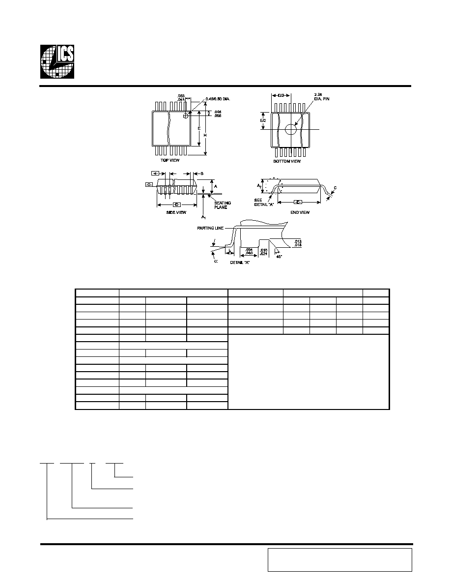
This table in inches
SSOP Package
SYMBOL
COMMON DIMENSIONS
VARIATIONS
D
N
MIN.
NOM.
MAX.
MIN.
NOM.
MAX.
A
.097
.101
.110
AA
.602
.607
612
36
A1
.008
.010
.0116
AB
.701
.706
.711
44
A2
.090
.092
.094
AC
.620
.625
.630
48
B
.0091
.014
.017
AD
.720
.725
.730
56
C
.0091
.010
.0125
D
See Variations
E
.292
.296
.299
e
.0315 BSC
H
.400
.406
.410
h
.010
.013
.016
L
.024
.032
.040
N
See Variations
0∞
5∞
8∞
X
.085
.093
.100
PRODUCT PREVIEW documents contain information on new
products in the sampling or preproduction phase of development.
Characteristic data and other specifications are subject to change
without notice.