Integrated
Circuit
Systems, Inc.
General Description
Features
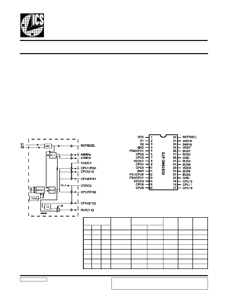
ICS9169C-272
Block Diagram
Frequency Generator for PentiumTM Based Systems
9169C-272RevC060297P
Pin Configuration
The ICS9169C-272 is a low-cost frequency generator
designed specifically for Pentium based chip set systems.
The integrated buffer minimizes skew and provides all the
clocks required. A 14.318 MHz XTAL oscillator provides
the reference clock to generate standard Pentium frequencies.
The CPU clock makes gradual frequency transitions without
violating the PLL timing of internal microprocessor clock
multipliers. A raised frequency setting of 68.5MHz is available
in the Turbo-mode of the 66.8MHz CPU. The ICS9169C-272
contains 12 CPU clocks, 4 PCI clocks, 1 REF at 48MHz and 1 at
24MHz.
The twelve CPU clock outputs provide sufficient clocks for
the CPU, chip set, memory and up to two DIMM connectors
(with four clocks to each DIMM). Either synchronous(CPU/
2) or asynchronous (32 MHz) PCI bus operation can be selected
by latching data on the BSEL input
32-Pin SOIC/SOJ
Pentium is a trademark of Intel Corporation.
∑
Twelve selectable CPU clocks operate up to 83.3MHz
∑
Maximum CPU jitter of ± 200ps
∑
Six BUS clocks support sync or async bus operation
∑
250ps skew window for CPU outputs, 500ps skew
window for BUS outputs
∑
CPU clocks BUS clocks skew 1-4ns (CPU early)
∑
Integrated buffer outputs drive up to 30pF loads
∑
3.0V - 3.7V supply range, CPU(1:6) outputs 2.5V(2.375-
2.62V) VDD option
∑
32-pin SOIC/SOJ package
∑
Logic inputs latched at Power-On for frequency selection
saving pins as Input/Output
∑
48 MHz clock for USB support and 24 MHz clock
for FD.
A D D R E S S
S E L E C T
C P U (1:12)
(M H z)
B U S (1:6)M H z
48M H z
24M H z
R E F
FS2 FS1
FS0
BSEL=1
BSEL=0
0
0
0
50
25
32
48
24
REF
0
0
1
60
30
32
48
24
REF
0
1
0
66.8
33.4
32
48
24
REF
0
1
1
75.9
32
32
48
24
REF
1
0
0
55
27.5
32
48
24
REF
1
0
1
75.9
37.5
32
48
24
REF
1
1
0
83.3
41.7
32
48
24
REF
1
1
1
68.5
34.25
32
48
24
REF
VDD Groups:
VDD1 = X1, X2, REF/BSEL
VDDC1 = CPU1-6
VDDC2 = CPU7-12 & PLL Core
VDDB = BUS1-6
VDDF = 48/24 MHz
Latched Inputs:
L1 = BSEL
L2 = FS0
L3 = FS1
L4 = FS2
ICS reserves the right to make changes in the device data identified in this
publication without further notice. ICS advises its customers to obtain the latest
version of all device data to verify that any information being relied upon by the
customer is current and accurate.
Functionality
3.3V±10%, 0-70
∞
C
Crystal (X1, X2) = 14.31818 MHz

2
ICS9169C-272
Pin Descriptions
PIN N UM BER
PIN N A M E
TYPE
DESCR IPTIO N
1
V D D
PW R
Power for device logic and crystal oscillator circuit and
14.318 M H z output.
2
X1
IN
XTAL or external reference frequency input. This input
includes XTA L load capacitance and feedback bias for a
12-16M Hz crystal, nom inally 14.31818M H z external crystal
load of 30pF to GND recom m ended for V D D pow er on faster
than 2.0m s.
3
X 2
OUT
XTAL output w hich includes XTAL load capacitance.
External crystal load of 10pF to GN D recom m ended for V DD
power on faster than 2.0m s.
4,11,20,26
G N D
PW R
Ground for device logic.
5
CPU (1)
OUT
Processor clock output which is a m ultiple of the input
reference frequency.
FS0
IN
Frequency m ultiplier select pins. 350K internal pull up.
6,7,9,10,15,16,17,18,19
CPU
(2:5) (8:12)
OUT
Processor clock outputs w hich are a m ultiple of the input
reference frequency.
8
V D DC1
PW R
Pow er for CPU (1:6) output buffers only. Can be reduced V DD
for 2.5V (2.375-2.62V ) next generation processor clocks.
12
CPU (6)
O UT
Processor clock output which is a m ultiple of the input
reference frequency internal pull up devices.
FS1
IN
Frequency m ultiplier select pin. See shared pin description.
350K internal pull up.
13
CPU (7)
OUT
Processor clock output which is a m ultiple of the input
reference frequency internal pull up devices.
FS2
IN
Frequency m ultiplier select pin. See shared pin description.
350K internal pull up.
14
VD D C2
PW R
Power for CPU PLL, logic and CPU(7:12)output buffers. M ust
be nom inal 3.3V (3.0 to 3.7V).
21,22,24,25,27,28
BUS (1:6)
OU T
BU S clock outputs w hich are a m ultiple of the input reference
clock.
23
VD D B
PW R
Power for BUS clock buffers BU S(1:6).
29
VD D F
PW R
Power for fixed clock buffer (48 M H z, 24 M hz).
30
24M H z
OUT
Fixed 24M Hz clock (assum ing a 14.31818M H z REF
frequency).
31
48M H z
OUT
Fixed 48M Hz clock (assum ing a 14.31818M H z REF
frequency).
32
REF
OU T
Fixed 14.31818M H z clock (assum ing a 14.31818M Hz REF
frequency).
BSEL
IN
Selection for synchronous or asynchronous bus clock
operation. See shared pin program m ing description late in this
data sheet for further explanation. 350K internal pull up.
* The internal pull up will vary from 350K to 500K based on temperature
3
ICS9169C-272
The ICS9169C-272 includes a production test verification
mode of operation. This requires that the FS0 and FS1 pins
be programmed to a logic high and the FS2 pin be
programmed to a logic low(see Shared Pin Operation
section). In this mode the device will output the following
frequencies.
Note: REF is the frequency of either the crystal connected
between the devices X1and X2 or, in the case of a device
being driven by an external reference clock, the frequency
of the reference (or test) clock on the device's X1 pin.
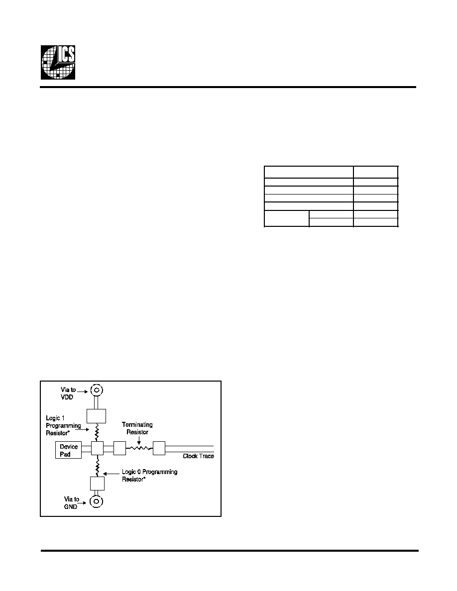
Shared Pin Operation - Input/Output Pins 5, 12, 13 and 32
on the ICS9169C-272 serve as dual signal functions to the
device. During initial power-up, they act as input pins.
The logic level (voltage) that is present on these pins at
this time is read and stored into a 4-bit internal data latch.
At the end of Power-On reset, (see AC characteristics for
timing values), the device changes the mode of operation
for these pins to an output function. In this mode the pins
produce the specified buffered clocks to external loads.
To program (load) the internal configuration register for
these pins, a resistor is connected to either the VDD (logic
1) power supply or the GND (logic 0) voltage potential. A
10 Kilohm(10K) resistor is used to provide both the solid
CMOS programming voltage needed during the power-up
programming period and to provide an insignificant load
on the output clock during the subsequent operating
period.
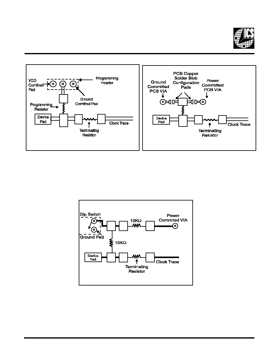
Figs. 1 and 2 show the recommended means of
implementing this function. In Fig. 1 either one of the
resistors is loaded onto the board (selective stuffing) to
configure the device's internal logic. Figs. 2a and b provide
a single resistor loading option where either solder spot
tabs or a physical jumper header may be used.
These figures illustrate the optimal PCB physical layout
options. These configuration resistors are of such a large
ohmic value that they do not effect the low impedance
clock signals. The layouts have been optimized to provide
as little impedance transition to the clock signal as possible,
as it passes through the programming resistor pad(s).
Shared Pin Operation -
Input/Output Pins
Test Mode Operation
Pin
Frequency
REF
REF
48MHz
REF/2
24MHz
REF/4
CPU (1:12)
REF2
BUS (1:6)
BSEL=1
REF/4
BSEL = 0
REF/3
Fig. 1
(Resistors are surface mount devices
shown schematically between 5.m. pads)
*use only one programming resistor
4
ICS9169C-272
Fig. 2a
Fig. 2b
Fig. 3

5
ICS9169C-272
Technical Pin Function Descriptions
VDD
This is the power supply to the internal logic of the device
as well as the following clock output buffers:
A. REF clock output buffers
B. BUS clock output buffers
C. Fixed clock output buffers
This pin may be operated at any voltage between 3.0 and
5.5 volts. Clocks from the listed buffers that it supplies
will have a voltage swing from ground to this level. For the
actual guaranteed high and low voltage levels of these
clocks, please consult the AC parameter table in this data
sheet.
GND
This is the power supply ground return pin for the internal
logic of the device as well as the following clock output
buffers:
A. REF clock output buffers
B. BUS clock output buffers
C. CPU clock output buffers
D. Fixed clock output buffers
X1
This pin serves one of two functions. When the device is
used with a crystal, X1 acts as the input pin for the
reference signal that comes from the discrete crystal.
When the device is driven by an external clock signal, X1
is the device' input pin for that reference clock. This pin
also implements an internal crystal loading capacitor that
is connected to ground. See the data tables for the value of
the capacitor.
X2
This pin is used only when the device uses a Crystal as the
reference frequency source. In this mode of operation, X2
is an output signal that drives (or excites) the discrete
crystal. This pin also implements an internal crystal loading
capacitor that is connected to ground. See the data tables
for the value of the capacitor.
CPU
This pin is the clock output that drives processor and other
CPU related circuitry that require clocks which are in tight
skew tolerance with the CPU clock. The voltage swing of
these clocks is controlled by that which is applied to the
VDDC pins of the device. See note on VDDC (1:2). See the
Functionality table at the beginning of this data sheet for
a list of the specific frequencies that this clock operates at
and the selection codes that are necessary to produce
these frequencies.
BUS
This pin is the clock output that is intended to drive the
systems plug-in card bus. The voltage swing of these
clocks is control-led by the supply that is applied to the
VDD pin of the device. See the Functionality table at the
beginning of this data sheet for a list of the specific
frequencies that this clock operates at and the selection
codes that are necessary to produce these frequencies.
FS0, FS1, FS2
These pins control the frequency of the clocks at the CPU,
CPUL, BUS & SDRAM pins. See the Funtionality table at
the beginning of this data sheet for a list of the specific
frequencies that this clock operates at and the selection
codes that are necessary to produce these frequencies.
The device reads these pins at power-up and stores the
programmed selection code in an internal data latch. (See
programming section of this data sheet for configuration
circuitry recommendations.
BSEL
This pin controls whether the BUS clocks will be
synchronous (run at half the frequency) with the CPU and
CPUL clocks or whether they will be asynchronous (run at
a pre-programmed fixed frequency) clock rate. It is a
shared pin and is pro grammed the same way as the
frequency select pins.
VDDC (1:2)
These are the power supply pins for the CPU (1:6) and
CPU (7:12) clock buffers. By separating the clock power
pins, each group can receive the appropriate power
decoupling and bypassing necessary to minimize EMI
and crosstalk between the individual signals. VDDCL can
be reduced to 2.5V VDD for advanced processor clocks,
which will bring CPU (1:6) outputs at 0 to 2.5V output
swings.
48 MHz
This is a fixed frequency clock that is typically used to
drive Super I/O peripheral device needs.
24 MHz
This is a fixed frequency clock that is typically used to
drive Keyboard controller clock needs.
REF
This is a fixed frequency clock that runs at the same
frequency as the input reference clock (typically 14.31818
MHz) is and typically used to drive Video and ISA BUS
requirements.
VDDB
This power pin supplies the BUS clock buffers.
VDDF
This power pin supplies the 48/24 MHz clocks.