Integrated
Circuit
Systems, Inc.
ICS91719
0506D--08/16/04
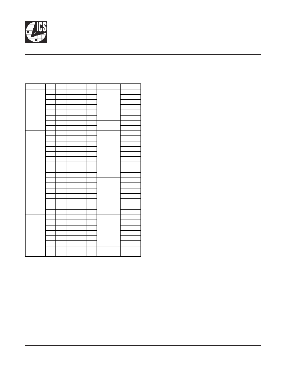
Block Diagram
Pin Configuration
16-pin TSSOP
Features:
∑
ICS91719 is a Spread Spectrum Clock targeted for
Mobile PC and LCD panel applications. Generates an
EMI optimized clock signal (EMI peak reduction of 7-
14 dB on 3rd-19th harmonics) through use of Spread
Spectrum techniques.
∑
ICS91719 focuses on the lower input frequency
range of 14.318 to 80.00 MHz with a spread
modulation of 20kHz to 40kHz.
Specifications:
∑
Supply Voltages: VDD = 3.3V ±0.3V
∑
Frequency range: 14.318 MHz
Fin
80 MHz
∑
Cyc to Cyc jitter: <150ps
∑
Output duty cycle 40/60% (worst case)
∑
Guarantees +85∞C operational condition.
∑
16-pin TSSOP package 4.4mm body (173mils), 0.65
mm pitch
∑
14.318 MHz crystal input or reference clock input
∑
27MHz, 48MHz and 66MHz reference clock input
Low EMI, Spread Modulating, Clock Generator
Notes:
** Internal pull-down
^ Internal pull-up
CLK
CL
REFOUT
KOUT
OUT
PD#
PD#
SPREAD#
SPREAD#
CLKIN
CLKIN
PLL1
PLL1
Spread
Spread
Spectr
Spectrum
um
SD
SDAT
REF_STOP
A
SCLK
SCLK
FS_IN0:1
Control
Control
Logic
Logic
Config.
Config.
Reg.
Reg.
REF Voltage Select Functionality
Input Select Functionality
GND
1
16
VDDREF
X1 _CLKIN
2
15
VDDREF_SEL_2.5V/3.3V# ^
X2
3
14
REF_OUT/VDDREF_SEL_1.8V * *
GNDA
4
13
**REF_Stop
VDDA
5
12
^PD#
VDD
6
11
SCLK
GND
7
10
SDATA
* * CLKOUT/FS_IN0
8
9
^SPREAD_ENABLE/FS_IN1
Pin14 Pin15
REF
Voltage
0 0
N/A
0 1
1.8V
1 0
2.5V
1 1
3.3V
FS_IN1 FS_IN0 MHZ
Default
Spread
%
0
0
14.318 in 27.00 out -0.8% downspread
0
1
14.318 in/out
-0.8% downspread
1
0
27.00 in/out
-0.8% downspread
1
1
48.00 in/out
66.66 in/out
-0.8% downspread
2
ICS91719
0506D--08/16/04
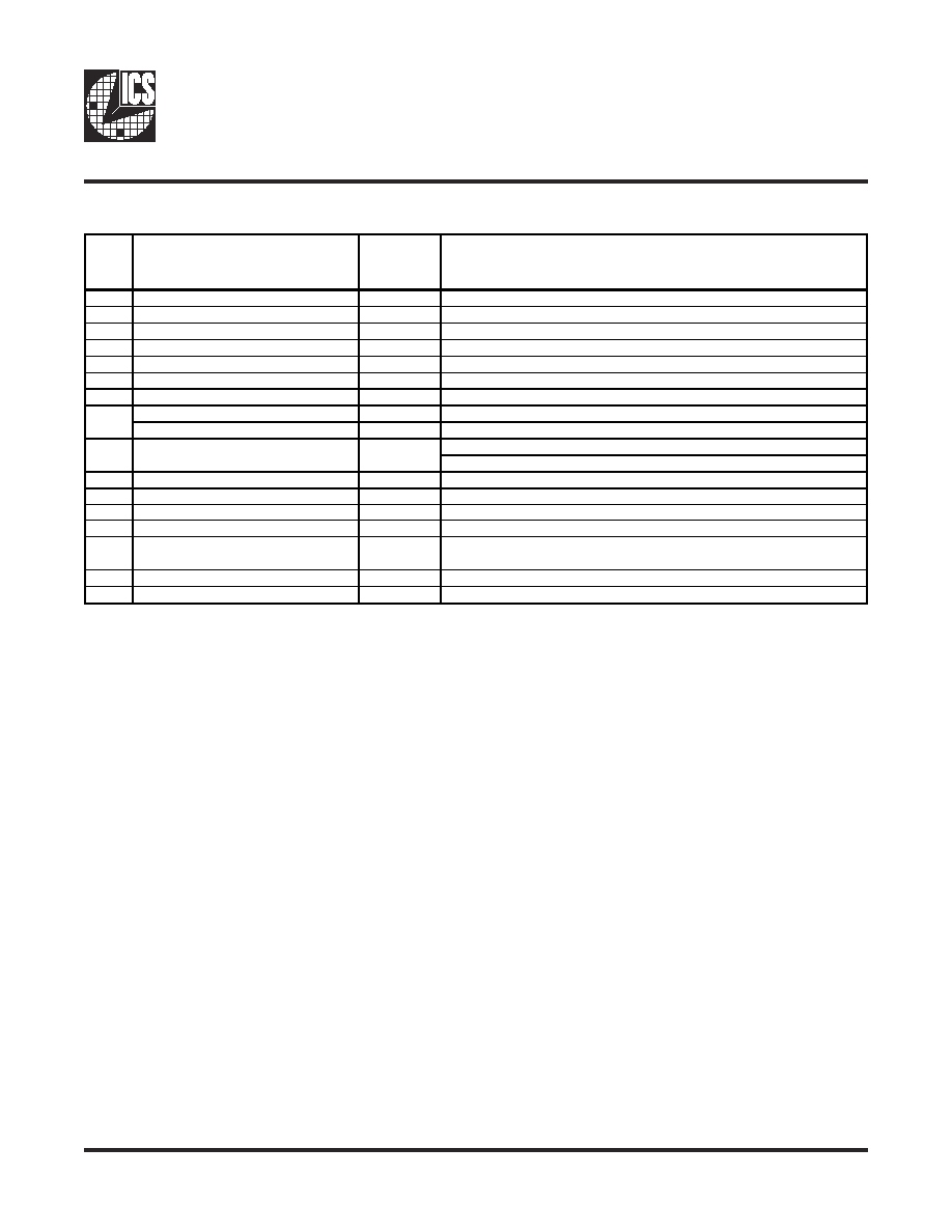
Pin Descriptions
PIN #
PIN NAME
PIN TYPE
DESCRIPTION
1
GND
PWR
Ground pin for 3V outputs
2
X1 _CLKIN
IN
Crystal input or CLOCKIN input
3
X2
OUT
Crystal output
4
GNDA
PWR
Analog ground
5
VDDA
PWR
Analog power supply for 3V
6
VDD
PWR
Power supply for 3V
7
GND
PWR
Ground pin for 3V outputs
CLKOUT
OUT
Modulated clock output
FS_IN0
IN
Latched input for input frequency select
Spread enable pin
Latched input for input frequency select
10
SDATA
IN
Data pin for I2C circuitry 5V tolerant
11
SCLK
IN
Clock pin for I2C circuitry 5V tolerant
12
^PD# IN
Power
down
13
**REF_Stop
IN
Stop control for REF_CLOCK output STOP:1, RUNNING:0
14
REF_OUT/VDDREF_SEL_1.8V * *
IN/OUT
REF_CLOCK output
15
VDDREF_SEL_2.5V/3.3V# ^
PWR
REF_CLOCK power supply voltage select
16
VDDREF
PWR
Power supply for REF_CLOCK
^internal pull-up
**internal pull-down
8
9
^SPREAD_ENABLE
FS_IN1
IN

4
ICS91719
0506D--08/16/04
1.
The ICS clock generator is a slave/receiver, I
2
C component. It can read back the data stored in the latches for
verification. Read-Back will support Intel PIIX4 "Block-Read" protocol.
2.
The data transfer rate supported by this clock generator is 100K bits/sec or less (standard mode)
3.
The input is operating at 3.3V logic levels.
4.
The data byte format is 8 bit bytes.
5.
To simplify the clock generator I
2
C interface, the protocol is set to use only "Block-Writes" from the controller.
The bytes must be accessed in sequential order from lowest to highest byte with the ability to stop after any
complete byte has been transferred. The Command code and Byte count shown above must be sent, but the
data is ignored for those two bytes. The data is loaded until a Stop sequence is issued.
6.
At power-on, all registers are set to a default condition, as shown.
Controller (Host)
ICS (Slave/Receiver)
Start Bit
Address
D2
(H)
ACK
Dummy Command Code
ACK
Dummy Byte Count
ACK
Byte 0
ACK
Byte 1
ACK
Byte 2
ACK
Byte 3
ACK
Byte 4
ACK
Byte 5
ACK
Byte 6
ACK
Byte 7
ACK
Stop Bit
How to Write:
Controller (Host)
ICS (Slave/Receiver)
Start Bit
Address
D3
(H)
ACK
Byte Count
ACK
Byte 0
ACK
Byte 1
ACK
Byte 2
ACK
Byte 3
ACK
Byte 4
ACK
Byte 5
ACK
Byte 6
ACK
Byte 7
Stop Bit
How to Read:
General I
2
C serial interface information
The information in this section assumes familiarity with I
2
C programming.
For more information, contact ICS for an I
2
C programming application note.
How to Write:
∑
Controller (host) sends a start bit.
∑
Controller (host) sends the write address D2
(H)
∑
ICS clock will
acknowledge
∑
Controller (host) sends a dummy command code
∑
ICS clock will
acknowledge
∑
Controller (host) sends a dummy byte count
∑
ICS clock will
acknowledge
∑
Controller (host) starts sending first byte (Byte 0)
through byte 6
∑
ICS clock will
acknowledge each byte one at a
time.
∑
Controller (host) sends a Stop bit
How to Read:
∑
Controller (host) will send start bit.
∑
Controller (host) sends the read address D3
(H)
∑
ICS clock will
acknowledge
∑
ICS clock will send the
byte count
∑
Controller (host) acknowledges
∑
ICS clock sends first byte
(Byte 0) through byte 7
∑
Controller (host) will need to acknowledge each
byte
∑
Controller (host) will send a stop bit
Notes: