Integrated
Circuit
Systems, Inc.
General Description
Features
ICS9212- 02
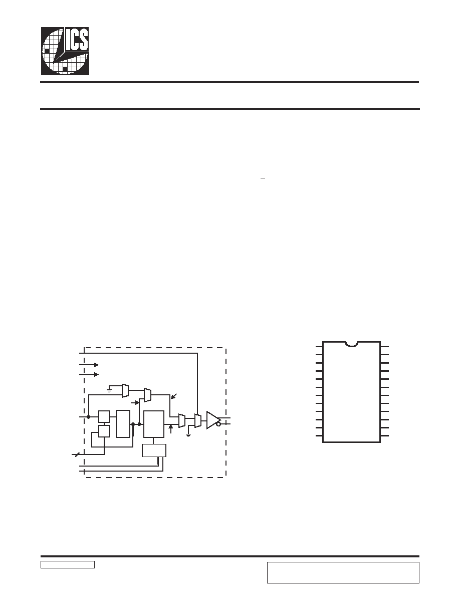
Block Diagram
Direct RambusTM Clock Generator
9212-02 Rev C 3/6/00
Pin Configuration
The ICS9212-02 is a High-speed clock generator providing
400 MHz differential clock source for direct Rambus
memory system. It includes DDLL (Distributed Delay locked
loop) and phase detection mechanism to synchronize the
direct Rambus
channel clock to an external system clock.
ICS9212-02 provides a solution for a broad range of Direct
Rambus memory applications. The device works in
conjunction with the ICS9250-09.
The ICS9212-02 power management support system turns
"off" the Rambus
channel clock to minimize power
consumption for mobile and other power ≠sensitive
applications. In "clock off" mode the device remains "on"
while the output is disabled, allowing fast transitions between
clock-off and clock ≠on states. In "power down" mode it
completely powers down for minimum power dissipation.
The ICS9212-02 meets the requirements for input frequency
tracking when the input frequency clock is using Spread
Spectrum clocking and also the optimum bandwidth is
maintained while attenuating the jitter of the reference signal.
24-Pin 150 Mil SSOP
∑
Compatible with all Direct RambusTM based IC s
∑
Up to 400 MHz differential clock source for direct
RambusTM memory system
∑
Cycle to cycle jitter is less than 50ps
∑
3.3 + 5% supply
∑
Synchronization flexibility: Supports Systems that
need clock domains of Rambus channel to synchronize
with system or processor clock, or systems that do not
require synchronization of the Rambus clock to
another system clock
∑
Excellent power management support
∑
REFCLK input is from the ICS9250-09.
BUSCLK_STOP#
PLL
Phase
Aligner
Pclk/M
Multi(0:1)
Synclk/N
PD#
FS(0:1)
Refclk
Test MUX
Bypass MUX
Bypclk
PLLclk
GND
GND
2
PAclk
BUSCLKT
BUSCLKC
B
A
Phase
Detector
VDDREF
REFCLK
VDD1
GND1
GND3
PCLK/M
SYNCLK/N
GND2
VDD2
VDDPD
BUSCLK_STOP#
PD#
FS0
FS1
VDD-OUT
GND-OUT
BUSCLKT
N/C
BUSCLKC
GND-OUT
VDD-OUT
MULTI0
MULTI1
GND3
ICS9212-02
1
2
3
4
5
6
7
8
9
10
11
12
24
23
22
21
20
19
18
17
16
15
14
13
Preliminary Product Preview
PRODUCT PREVIEW documents contain information on new
products in the sampling or preproduction phase of development.
Characteristic data and other specifications are subject to change
without notice.

2
ICS9212-02
Preliminary Product Preview
dvance Information
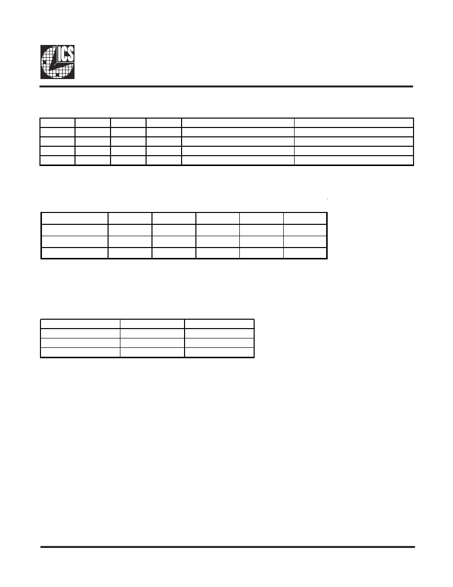
Pin Descriptions
Pin #
Name
Type
Description
1
VDDREF
REFV
Reference voltage for refclk, to be connected to CK133
2
REFCLK
IN
Reference clock, to be connected to CK133
3
VDD1
PWR
3.3 V power supply used for PLL
4
GND1
PWR
Ground for PLL
5, 13
GND3
PWR
Ground for control inputs
6,7
PCLK/M, SYNCLK/N
IN
Phase controller input, used to drive a phase aligner
that adjusts the phase of the busclk.
8
GND2
PWR
Ground for phase aligner
9
VDD2
PWR
3.3 V power supply used for phase aligner
10
VDDPD
REFV
Reference voltage for phase detector inputs connected
to the controller
11
BUSCLK_ STOP#
IN
Active low output enable/disable
12
PD#
IN
3.3V CMOS active low power down, the device is
powered down when the "(PD#) =0"
14,15
MULTI (0:1)
IN
3.3V CMOS PLL Multiplier select, logic for selecting the
multiply ratio for the PLL from the input REFCLK
16
VDD_OUT
PWR
3.3V supply for clock out puts
17
GND_OUT
PWR
Ground for clock outputs
18
BUSCLKC
OUT
Out put clock connected to the Rambus channel. This
output is the complement of BUSCLK
19
N/C
N/C
NOT USED
20
BUSCLKT
OUT
Out put clock connected to the Rambus channel. This
output is the true component of BUSCLK
21
GND_OUT
PWR
Ground for clock outputs
22
VDD_OUT
PWR
3.3V supply for clock out puts
24, 23
FS(0:1)
IN
3.3V CMOS Mode control, used in selecting bypass,
test, normal, and output test (OE)
3
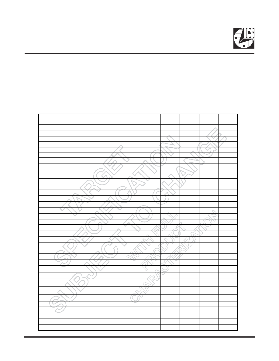
ICS9212- 02
Preliminary Product Preview
Mult0
Mult1
A
B
PLLCLK for REFCLK=50MHz
PLLCLK for REFCLK=66.67MHz
0
0
9
2
225.00
300.02
0
1
6
1
300.00
400.02
1
0
16
3
266.67
355.57
1
1
8
1
400.00
Reserved
PLL DIVIDER SELECTION AND PLL VALUES ( PLLCLK = REFCLK*A/B)
POWER MANAGEMENT MODES
State
PwrDnB
StopB
NORMAL
1
1
Clk Off
1
0
Powerdown
0
X
Mode FS0
FS1
Bypclk
(int.)
BusClk
BusClkB
Normal
0
0
Gnd
PAclk
PAclkB
Bypass 1
0
PLLclk
PLLclk
PLLclkB
Test
1
1
Refclk
Refclk
RefclkB
BYPASS AND TEST MODE SELECTION
4
ICS9212-02
Preliminary Product Preview
dvance Information
Absolute Maximum Ratings
Supply Voltage . . . . . . . . . . . . . . . . . . . . . . . . . . . . 4.0 V
Logic Inputs . . . . . . . . . . . . . . . . . . . . . . . . . . . . . . GND ≠0.5 V to V
DD
+0.5 V
Ambient Operating Temperature . . . . . . . . . . . . . 0∞C to +70∞C
Storage Temperature . . . . . . . . . . . . . . . . . . . . . . . ≠65∞C to +150∞C
Stresses above those listed under Absolute Maximum Ratings may cause permanent damage to the device. These ratings are
stress specifications only and functional operation of the device at these or any other conditions above those listed in the
operational sections of the specifications is not implied. Exposure to absolute maximum rating conditions for extended
periods may affect product reliability.
Parameters
Symbol
Min
Max
Unit
Supply Voltage
VDD
3.15
3.45
V
Refclk Input cycle time
t
CY CLE,IN
10
40
ns
Input cycle-to-cycle Jitter
t
J,IN
-
250
ps
Input Duty cycle over 10k cycles
DC
IN
40%
60%
t
CY CLE
Input frequency of modulation
F
m,in
30
33
KHz
Modulation index
P
M,IN
0.25
0.5
%
Phase detector input cycle time at PDclk/M & Synclk/N
t
CY CLE,PD
30
100
ns
Initial phase error at phase detector inputs
T
err,init
-0.5
0.5
t
CY CLE,PD
Phase detector input duty cycle over 10k cycles
D
CIN,PD
25%
75%
t
CY CLE,PD
Input rise & fall times ( measured at 20%-80% of input voltage) for
PDCLK/M & SYNCLK/N,&REfCLK
T
IR
,T
IF
-
1
ns
Input capacitance at PDCLK/M,Synclk/N,&REFCLK
C
IN,PD
-
7
pF
Input Capacitance matching at PCLK/M & SYNCLK/N
C
IN,PD
-
0.5
pF
Input capacitance at CMOS pins
C
IN,CMOS
-
10
pF
Input (CMOS) signal low voltage
V
IL
-
0.3
Vdd
Input (CMOS) signal high voltage
V
IH
0.7
-
Vdd
REFCLK input low voltage
V
IL,R
-
0.3
Vddi,R
REFCLK input high voltage
V
IH,R
0.7
-
Vddi,R
Input signal low voltage for PD inputs and STOP
V
IL,PD
-
0.3
Vddi,PD
Input signal high voltage for PD inputs and STOP
V
IH,PD
0.7
-
Vddi,PD
Input supply referance for REFCLK
V
DD,IR
1.3
3.3
V
Input supply referance vfor PD inputs
V
DDI,PD
1.3
3.3
V
Phase detector phase error for distributed loop measured at
PDCLK/M & SYNCLK/N(rising
t
ERR,PD
-100
100
ps
Cycle cycle time
t
CY CLE
2.5
3.75
ns
Cycle-to-cycle jitter at Busclk/BUSCLKB
t
J
-
50
ps
Total jitter over 2,3, or 4clock cycles
tJ
-
100
ps
Phase aligner, phase step size (BSCLK/BUSCLKB)
t
STEP
1
-
ps
PLL out put phase error when tracking SSC
t
ERR,SSC
-100
100
ps
Out put crossing-point voltage
V
X
1.3
1.8
V
Output voltage swing
V
COS
0.4
0.6
V
Output high voltage
V
H
-
2
V
Out put duty cycle over 10k cycle
DC
40%
60%
t
CY CLE
Output cycle -to-cycle duty cycle error
t
DC,ERR
-
50
ps
Output rise & fall times ( measured at 20%-80% of output voltage)
t
CR
,t
CF
300
500
psd
Difference between rise and fall times on a single device(20%-80%)
t
CR,CF
-
100
ps
Electrical Characteristics-input/supply/Outputs
5
ICS9212- 02
Preliminary Product Preview
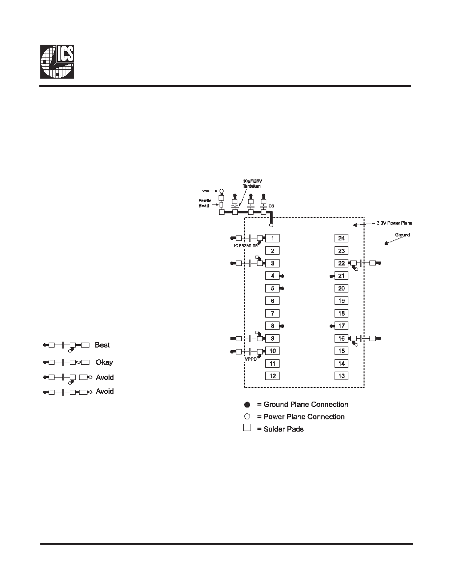
General Layout Precautions:
1) Use a ground plane on the top layer of
the PCB in all areas not used by traces.
2) Make all power traces and vias as wide as
possible to lower inductance.
Connections to VDD:
Capacitor Values:
C3 : 100pF ceramic
All unmarked capacitors are 0.01µF ceramic