 | –≠–ª–µ–∫—Ç—Ä–æ–Ω–Ω—ã–π –∫–æ–º–ø–æ–Ω–µ–Ω—Ç: ICS9214 | –°–∫–∞—á–∞—Ç—å:  PDF PDF  ZIP ZIP |
Integrated
Circuit
Systems, Inc.
ICS9214
0809D≠04/07/06
Block Diagram
Rambus
TM
XDR
TM
Clock Generator
The ICS9214 clock generator provides the necessary clock
signals to support the Rambus XDR
TM
memory subsystem
and Redwood logic interface. The clock source is a reference
clock that may or may not be modulated for spread spectrum.
The ICS9214 provides 4 differential clock pairs in a space
saving 28-pin TSSOP package and provides an off-the-shelf
high-performance interface solution.
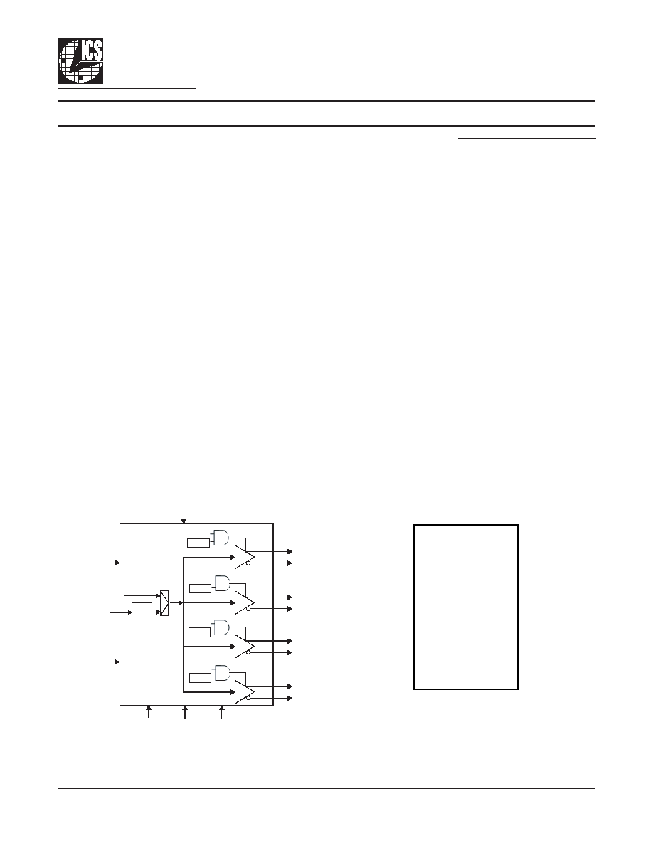
Figure 1 shows the major components of the ICS9214 XDR
Clock Generator. These include the a PLL, a Bypass
Multiplexer and four differential output buffers. The outputs
can be disabled by a logic low on the OE pin. An output is
enabled by the combination of the OE pin being high, and 1
in its SMBus Output control register bit.
The PLL receives a reference clock, CLK_INT/C and outputs
a clock signal at a frequency equal to the input frequency
times a multiplier. Table 2 shows the multipliers selectable
via the SMBus interface. This clock signal is then fed to the
differential output buffers to drive the enabled clocks. Disabled
outputs are set to Hi-Z. The Bypass mode routes the input
clock, CLK_INT/C, directly to the differential output buffers,
bypassing the PLL.
Up to four ICS9214 devices can be cascaded on the same
SMBus. Table 3 shows the SMBus addressing and control for
the four devices.
∑
400 ≠ 500 MHz clock source
∑
4 open-drain differential output drives with short term
jitter < 40ps
∑
Spread spectrum compatible
∑
Reference clock is differential or single-ended, 100 or
133 MHz
∑
SMBus programmability for:
- frequency multiplier
- output enable
- operating mode
∑
Supports frequency multipliers of: 3, 4, 5, 6, 8, 9/2,
15/2 and 15/4
∑
Support systems where XDR subsystem is
asynchronous to other system clocks
∑
2.5V power supply
PLL
Bypass
MUX
RegA
RegB
RegC
RegD
CLK_INT
CLK_INC
SMBCLK
OE
OE
OE
OE
OE
BYPASS#/PLL
SMBDAT SMB_A0 SMB_A1
ODCLK_C3
ODCLK_T3
ODCLK_C2
ODCLK_T2
ODCLK_C1
ODCLK_T1
ODCLK_C0
ODCLK_T0
AVDD2.5
1
28 VDD2.5
AGND
2
27 ODCLK_T0
IREFY
3
26 ODCLK_C0
AGND
4
25 GND
CLK_INT
5
24 ODCLK_T1
CLK_INC
6
23 ODCLK_C1
VDD2.5
7
22 VDD2.5
GND
8
21 GND
SMBCLK
9
20 ODCLK_T2
SMBDAT 10
19 ODCLK_C2
OE 11
18 GND
SMB_A0 12
17 ODCLK_T3
SMB_A1 13
16 ODCLK_C3
BYPASS#/PLL 14
15 VDD2.5
I
C
S
921
4
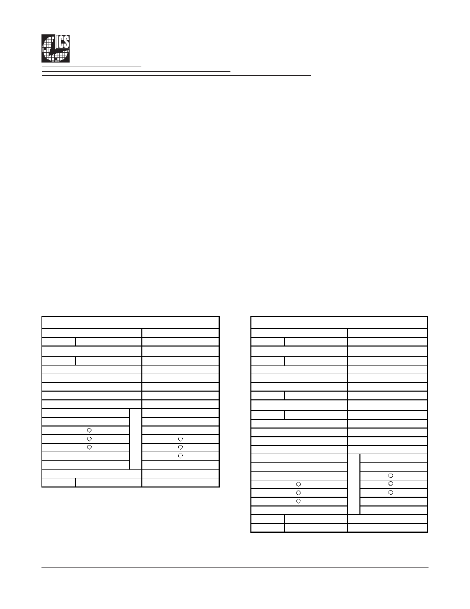
Pin Configuration
28-Pin 4.4mm TSSOP
General Description
Features

2
Integrated
Circuit
Systems, Inc.
ICS9214
0809D--04/07/06
Pin Descriptions
PIN #
PIN NAME
PIN TYPE
DESCRIPTION
1
AVDD2.5
PWR
2.5V Analog Power pin for Core PLL
2
AGND
PWR
Analog Ground pin for Core PLL
3
IREFY
OUT
This pin establishes the reference current for the differential
clock pairs. This pin requires a fixed precision resistor tied to
ground in order to establish the appropriate current.
4
AGND
PWR
Analog Ground pin for Core PLL
5
CLK_INT
IN
"True" reference clock input.
6
CLK_INC
IN
"Complementary" reference clock input.
7
VDD2.5
PWR
Power supply, nominal 2.5V
8
GND
PWR
Ground pin.
9
SMBCLK
IN
Clock pin of SMBUS circuitry, 5V tolerant
10
SMBDAT
I/O
Data pin of SMBUS circuitry, 5V tolerant
11
OE
IN
Active high input for enabling outputs.
0 = tri-state outputs, 1= enable outputs
12
SMB_A0
IN
SMBus address bit 0 (LSB)
13
SMB_A1
IN
SMBus address bit 1
14
BYPASS#/PLL
IN
Input to select Bypass(fan-out) or PLL (ZDB) mode
0 = Bypass mode, 1= PLL mode
15
VDD2.5
PWR
Power supply, nominal 2.5V
16
ODCLK_C3
OUT
"Complementary" side of open drain differential clock output.
This open drain output needs an external resistor network..
17
ODCLK_T3
OUT
"True" side of open drain differential clock output. This open
drain output needs an external resistor network..
18
GND
PWR
Ground pin.
19
ODCLK_C2
OUT
"Complementary" side of open drain differential clock output.
This open drain output needs an external resistor network..
20
ODCLK_T2
IN
"True" side of open drain differential clock output. This open
drain output needs an external resistor network..
21
GND
IN
Ground pin.
22
VDD2.5
PWR
Power supply, nominal 2.5V
23
ODCLK_C1
OUT
"Complementary" side of open drain differential clock output.
This open drain output needs an external resistor network..
24
ODCLK_T1
OUT
"True" side of open drain differential clock output. This open
drain output needs an external resistor network..
25
GND
PWR
Ground pin.
26
ODCLK_C0
OUT
"Complementary" side of open drain differential clock output.
This open drain output needs an external resistor network..
27
ODCLK_T0
OUT
"True" side of open drain differential clock output. This open
drain output needs an external resistor network..
28
VDD2.5
PWR
Power supply, nominal 2.5V
3
Integrated
Circuit
Systems, Inc.
ICS9214
0809D--04/07/06
General SMBus serial interface information for the ICS9214
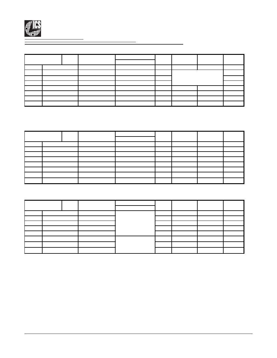
How to Write:
∑ Controller (host) sends a start bit.
∑ Controller (host) sends the write address D8
(H)
∑ ICS clock will
acknowledge
∑ Controller (host) sends the begining byte location = N
∑ ICS clock will
acknowledge
∑ Controller (host) sends the data byte count = X
∑ ICS clock will
acknowledge
∑ Controller (host) starts sending
Byte N through
Byte N + X -1
(see Note 2)
∑ ICS clock will
acknowledge each byte one at a time
∑ Controller (host) sends a Stop bit
How to Read:
∑ Controller (host) will send start bit.
∑ Controller (host) sends the write address D8
(H)
∑ ICS clock will
acknowledge
∑ Controller (host) sends the begining byte
location = N
∑ ICS clock will
acknowledge
∑ Controller (host) will send a separate start bit.
∑ Controller (host) sends the read address D9
(H)
∑ ICS clock will
acknowledge
∑ ICS clock will send the data byte count = X
∑ ICS clock sends
Byte N + X -1
∑ ICS clock sends
Byte 0 through byte X (if X
(H)
was written to byte 8)
.
∑ Controller (host) will need to acknowledge each byte
∑ Controllor (host) will send a not acknowledge bit
∑ Controller (host) will send a stop bit
ICS (Sla ve/Re ce ive r)
T
W R
ACK
ACK
ACK
ACK
ACK
P
Byte N + X - 1
Data Byte Count = X
Beginning Byte N
stoP bit
X B
y
te
Index Block Write Operation
Slave Address D8
(H )
Beginning Byte = N
W Rite
starT bit
Controlle r (Host)
T
starT bit
W R
W Rite
RT
Repeat starT
RD
ReaD
Beginning Byte N
Byte N + X - 1
N
Not acknowledge
P
stoP bit
ICS (Sla ve/Re ce ive r)
Controlle r (Host)
X Byte
ACK
ACK
Data Byte Count = X
ACK
Slave Address D9
(H )
Index Block Read Operation
Slave Address D8
(H )
Beginning Byte = N
ACK
ACK
4
Integrated
Circuit
Systems, Inc.
ICS9214
0809D--04/07/06
SMB Table: Output Control Register
Control
Function
Bit 7
Test Mode
Reserved for Vendor
RW
0
Bit 6
MULT2
Multiplier Select
RW
0
Bit 5
MULT1
Multiplier Select
RW
0
Bit 4
MULT0
Multiplier Select
RW
1
Bit 3
ODCLK_T/C0
Output Control
RW
1
Bit 2
ODCLK_T/C1
Output Control
RW
1
Bit 1
ODCLK_T/C2
Output Control
RW
1
Bit 0
ODCLK_T/C3
Output Control
RW
1
Disable = Output in high-impedance state
Enable = Output is switching
SMB Table: Frequency Multiplier Control Register
Control
Function
Bit 7
Reserved
Reserved
RW
0
Bit 6
Reserved
Reserved
RW
0
Bit 5
Reserved
Reserved
RW
0
Bit 4
Reserved
Reserved
RW
0
Bit 3
Reserved
Reserved
RW
0
Bit 2
Reserved
Reserved
RW
0
Bit 1
Reserved
Reserved
RW
0
Bit 0
Test Mode
Reserved for Vendor
RW
0
SMB Table: Revision & Vendor ID Register
Control
Function
Bit 7
RID4
R
X
Bit 6
RID3
R
X
Bit 5
RID2
R
X
Bit 4
RID1
R
X
Bit 3
RID0
R
X
Bit 2
VID2
R
0
Bit 1
VID1
R
0
Bit 0
VID0
R
1
NOTES:
1. PWD = Power Up Default
Disable
Enable
-
-
-
-
-
-
-
-
-
-
Vendor ID
-
-
-
-
-
Revision ID
-
-
-
-
-
-
0
1
See Table 2.
PWD
1
PWD
-
-
-
Byte 2
Pin #
Name
Type
-
-
Byte 0
Pin #
Name
Type
Disable
Enable
0
1
-
-
Byte 1
Pin #
-
27,26
24,23
20,19
17,16
-
-
-
Name
Type
0
1
-
-
-
-
-
-
-
-
-
-
-
-
-
-
PWD
Disable
Enable
Disable
Disable
Enable
Enable
Disable
Enable
5
Integrated
Circuit
Systems, Inc.
ICS9214
0809D--04/07/06
Device ID and SMBus Device Address
The device ID (SMB_A(1:0)) is part of the SMBus device address. The least significant bit of the address designates a write
or read operation. Table 3 shows the addresses for four ICS9214 devices on the same SMBus.
PLL Multiplier
Table 2 shows the frequency multipliers in the PLL, selectable by programming the MULT0, MULT1 and MULT2 bits in the
SMBus Multiplier Control register. Power up default is 4.
Table 2. PLL Multiplier Selection
Bit 6
Bit 5
Bit 4
MULT2
MULT1
MULT0
0
0
0
3
300
3
400
0
0
1
4
400
2
533
0
1
0
5
500
667
0
1
1
6
600
800
1
0
0
8
800
-
3
1
0
1
9/2
450
600
1
1
0
15/2
750
-
3
1
1
1
15/4
375
500
NOTES
1 Output frequencies are based on nominal input frequencies of 100 MHz and 133 MHz. The PLL
multipliers are also applicable to spread spectrum modulated input clocks.
2 Default muliplier value at power up
3 Outputs at these settings do not conform to the AC Output Characteristics, or are not supported.
4 Shaded areas are under development and are not yet supported
Byte 0
Output Frequency (MHz)
Frequency
Multiplier
CLK_INT/C =
100 MHz
1
CLK_INT/C =
133 MHz
1
Table 3. SMBus Device Addresses
Device
Operation
SMB_A1
SMB_A0
WR#/RD
Write
D8
0
Read
D9
1
Write
DA
0
Read
DB
1
Write
DC
0
Read
DD
1
Write
DE
0
Read
DF
1
0
2
ICS9214
Hex Address
0
1
3
8-bit SMBus Device Address, Including Oper.
1
11011
1
0
0
1
1
0