 | –≠–ª–µ–∫—Ç—Ä–æ–Ω–Ω—ã–π –∫–æ–º–ø–æ–Ω–µ–Ω—Ç: ICS9219 | –°–∫–∞—á–∞—Ç—å:  PDF PDF  ZIP ZIP |

Integrated
Circuit
Systems, Inc.
General Description
Features
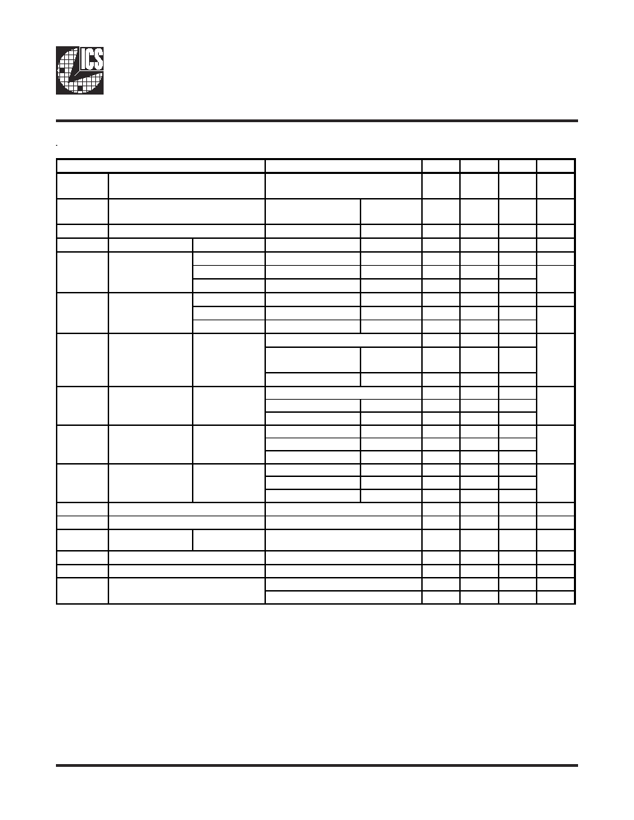
ICS9219
0931B--10/25/04
Block Diagram
Direct RambusTM Clock Generator Lite
ICS9219 is a High-speed clock generator providing 400 or
533 MHz differential clock source for direct Rambus
memory system. ICS9219 takes a crystal as an input
reference source, and produces the differential output
clock required for the Rambus channel. ICS9219 provides
a solution for a broad range of Direct Rambus memory
applications. ICS9219 can be used in single or dual
Rambus channels. An additional LVCMOS output, which
provides a reference clock at the crystal frequency for the
other system blocks is also included.
∑
Compatible with all Direct Rambus
TM
based ICs
∑
Provides differential clock source for direct
Rambus
memory system with 1GHz data transfer
rate capability
∑
Cycle to Cycle jitter is less than 100ps
∑
3.3V + 4% supply
∑
LVCMOS REF clock @ crystal frequency
∑
Output edge rate control to minimize EMI
PLL
Control
Logic
Xtal
OSC
FS0
X1
X2
FS1
VDDT
FS2
BUSCLKT
BUSCLKC
REF
VDDT 1
16 FS0*
GND 2
15 VDD
X2 3
14 GND
X1 4
13 BUSCLKT
VDD 5
12 BUSCLKC
REF 6
11 GND
GND 7
10 VDD
FS1* 8
9 FS2*
IC
S9219
Pin Configuration
16-Pin 173 mil TSSOP
* Pins have 60K internal pull-up to VDD
Table 1. PLL Multiplier Selection and Output Frequency
FS0
Mult
BUSCLK
1
0
16
400.00
1
21.33
2
533.30
Notes:
1 Output frequencies are based on 25MHz XTAL Input
multipliers are also applicable to spread spectrum modulated input clocks.
2 Default muliplier value at power up.

2
ICS9219
0931B--10/25/04
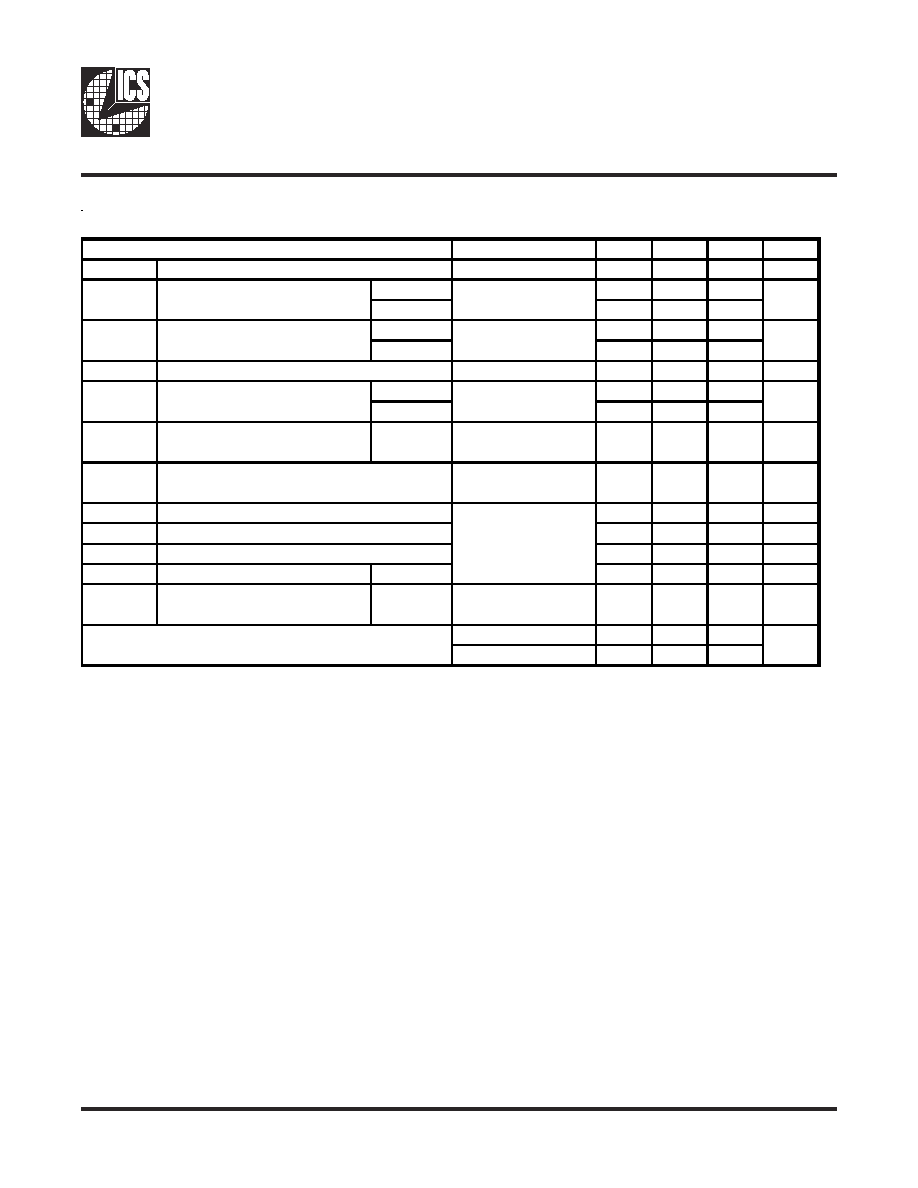
Pin Descriptions
PIN #
PIN NAME
PIN TYPE
DESCRIPTION
1
VDDT
PWR/IN
Power supply, nominal 3.3V/Test mode
2
GND
PWR
Ground pin.
3
X2
OUT
Crystal output (14MHz to 25MHz)
4
X1
IN
Crystal input (14MHz to 25MHz)
5
VDD
PWR
Power supply, nominal 3.3V
6
REF
OUT
Reference of Input
7
GND
PWR
Ground pin.
8
FS1*
IN
Frequency select pin.
9
FS2*
IN
Real-time frequency select pin with internal 120Kohm pull-up resistor (check
SMBus HW/SW setting for priority).
10
VDD
PWR
Power supply, nominal 3.3V
11
GND
PWR
Ground pin.
12
BUSCLKC
OUT
Output clock connected to the Rambus channel. This output is the complement
of BUSCLK.
13
BUSCLKT
OUT
Output clock connected to the Rambus channel. This output is the true
component of BUSCLK.
14
GND
PWR
Ground pin.
15
VDD
PWR
Power supply, nominal 3.3V
16
FS0*
IN
Frequency select pin.
* Pins have 60K internal pull-up to VDD
Table 2: Function Table
FS2
FS1
FS0
3.3V
0
0
0
16
NORMAL
INPUT x MULT
BUSCLKC
INPUT
3.3V
1
1
1
21.33
NORMAL
INPUT x MULT
BUSCLKC
INPUT
3.3V
1
1
0
16
NORMAL
INPUT x MULT
BUSCLKC
INPUT
3.3V
0
0
1
21.33
NORMAL
INPUT x MULT
BUSCLKC
INPUT
3.3V
1
0
X
-
TEST
BUSCLKT/2
BUSCLKC/2
INPUT
3.3V
0
1
X
-
TEST
BUSCLKT/4
BUSCLKC/4
INPUT
0
0
0
X
-
TEST
X1
X1(INVERT)
INPUT
0
1
1
X
-
TEST
X1
X1(INVERT)
INPUT
0
1
0
X
-
TEST
X1/2
X1(INVERT)/2
INPUT
0
0
1
X
-
TEST
X1/4
X1(INVERT)/4
INPUT
BUSCLKC
REF
VDDT
FS(2:0)
INPUT
MULT
MODE
BUSCLKT

3
ICS9219
0931B--10/25/04
Absolute Maximum Ratings over operating free-air temperature
Supply voltage range, V
DD
or V
DDT
(see Note 1)
-0.5 V to 4 V
. . . . . . . . . . . . . . . . . . . . . . . . . . . . . . . . . . . . . .
Input voltage range,V
I
, at any input terminal
-0.5 V to V
DD
+ 0.5 V
. . . . . . . . . . . . . . . . . . . . . . . . . . . . . . . . . . . .
Output voltage range, V
O
, at any output terminal (BUSCLKT/C)
-0.5 V to V
DD
+ 0.5 V
. . . . . . . . . . . . . . . . . . . .
ESD rating (MIL-STD 883C, Method 3015)
> 2 kV, Machine Model >200 V
. . . . . . . . . . . . . . . . . . . . . . . . . . . . .
Operating free-air temperature range, T
A
∞C to 85∞C
. . . . . . . . . . . . . . . . . . . . . . . . . . . . . . . . . . . . . . . . . . . . . .
Storage temperature range, T
stg
-65∞
C to 150∞C
. . . . . . . . . . . . . . . . . . . . . . . . . . . . . . . . . . . . . . . . . . . . . . . . . . .
Stresses beyond those listed under absolute maximum ratings may cause permanent damage to the device. These are stress ratings only, and
functional operation of the device at these or any other conditions beyond those indicated under recommended operating conditions is not
implied. Exposure to absolute-maximum-rated conditions for extended periods may affect device reliability.
NOTE 1: All voltage values are with respect to the GND terminals.
0
Recommended Operating Conditions
MIN
NOM
MAX
UNIT
3
3.3
3.6
V
Low-level input voltage, V
IL
FS (2:0)
0.35 x V
DD
High-level input voltage, V
IH
FS (2:0)
0.65 x V
DD
Internal pullup resistance
FS (2:0)
90
150
k
14.0625
25
26
MHz
BUSCLKT/C
16
REF
10
BUSCLKT/C
-16
REF
-10
FS (2:0)
15
X1, X2
15
0
85
C
Supply voltage, V
DD
High-level output current, I
OH
Operating free-air temperature
pF
Input capacitance (CMOS), C
L
V
mA
mA
Low-level output current, I
OL
Input frequency at crystal input
Timing Requirements
MIN
MAX
UNIT
Clock cycle time, t
(CYCLE)
2.5
3.7
ns
Input slew rate, S
R
0.5
4
V/ns
State transition latency (V
DDX
or S0 to CLKs - normal mode), t
(STL)
3
ms
Crystal Specifications
MIN
MAX
UNIT
Frequency
14.0625
26
MHz
Frequency tolerance (at 25∞C) ± 3∞C)
-15
15
ppm
Equivalent resistance (C
L
= 10 pF)
100
Temperature drift (-10∞C to 75∞C)
10
ppm
Drive level
0.01
1500
µ
Motional inductance
20.7
25.3
mH
Insulation resistance
500
M
Spurious attenuation ratio (at frequency ±500 kHz)
3
dB
Overtone spurious
8
dB
4
ICS9219
0931B--10/25/04
MIN
TYP**
MAX
UNIT
V
X
1.25
1.6
1.85
V
V
COS
V
OH
- V
OL
See Figure 1
0.4
0.6
0.7
V
V
IK
V
DD
= 3V
I
I
= -18 mA
-1.2
V
R
I
Input res istanc e
X1, X2
V
DD
= 3.3V
V
I
= V
O
>50
k
X2
V
DD
= 3.3V
V
O
= 2V
27
mA
FS0
V
DD
= 3.6V
V
I
= V
DD
10
FS1, FS2
V
DD
= 3.6V
V
I
= V
DD
10
X2
V
DD
= 3.6V
V
O
= 0V
-5.7
mA
FS0
V
DD
= 3.6V
V
I
= 0V
-30
-100
FS1, FS2
V
DD
= 3.6V
V
I
= 0V
-10
-50
2.1
V
DD
= min to max
I
OH
= -1 mA
V
DD
-
0.1V
V
DD
= 3V
I
OH
= -16 mA
2.2
2.5
1
V
DD
= min to max
I
OH
= 1 mA
0.05
0.1
V
DD
= 3V
I
OH
= 16 mA
0.25
0.5
V
DD
= 3.135V
V
O
= 1V
-50
-32
V
DD
= 3.3V
V
O
= 1.65V
-50
V
DD
= 3.465V
V
O
= 3.135V
-21
-15
V
DD
= 3.135V
V
O
= 1.95V
43
69
V
DD
= 3.3V
V
O
= 1.65V
69
V
DD
= 3.465V
V
O
= 0.9V
30
36
r
OH
12
25
40
r
OL
12
17
40
C
O
O utput capacitance
BUSCLKT,
BUSCLKC, REF
3
pF
I
DD
6.5
mA
I
DDL
50
mA
84
100
mA
91
120
mA
Static supply c urrent
Static supply c urrent
I
OL
I
OH
Low-level output
c urrent
BUSCLKT/C,
REF
High-level dynamic output res istance
4
Low-lev el dy namic output resis tanc e
4
400 MHz
533MHz
See Figure 1
V
O utputs high or low (V
DDT
= 0V)
O utputs high or low (V
DDT
= 0V)
I
O
- 14.5 mA to
I
O
- 16.5 mA
I
O
- 14.5 mA to
I
O
- 16.5 mA
BUSCLKT/C,
REF
Low-level input
current
V
OL
Low-level output
v oltage
V
OH
mA
mA
I
IL
PARAMETER
See Figures 1 and 2
Electrical Characteristics over Recommended Operating Free-Air Temperature
* V
DD
refers to any of the following: V
DD,
V
DDT
.
** All ty pic al values are at V
DD
= 3.3V, T
A
25∞C.
4
r
O
=
V
O
/
I
O
. This is defined at the output terminals , not at the measurement point of figure 1.
TEST CO NDITIO NS*
I
IH
High-level input
current
Differential crossing-point output
v oltage
Peak-to-peak output voltage swing,
s ingle ended
Input clamp voltage
I
DD (NORMA L)
Supply current in normal state
See Figure 1
V
BUSCLKT/C,
REF
High-lev el output
v oltage
mA
mA
High-lev el output
c urrent
BUSCLKT/C,
REF
5
ICS9219
0931B--10/25/04
Switching Characteristics over Recommended Operating Free-Air Temperature Range.
MIN
TYP**
MAX
UNIT
t
(CYCLE)
1.8
3.7
ns
400 MHz
42
50
533 MHz
33
50
400 MHz
300
533 MHz
300
D
C
43%
51
53%
400 MHz
30
50
533 MHz
30
50
t
CR
, t
DF
Output rise and fall times (measured at
20%-80% of output voltage)
BUSCLKT/C
120
250
400
ps
t
RF
50
100
ps
t
CYCLE(L)
80
142.2
ns
t
(CJ)
-0.2
0.1
0.2
ns
t
(CJ10)
-1.3 t
(CJ)
1.3 t
(CJ)
ns
D
C(2)
Output duty cycle
REF
47%
50
53%
t
CRL
, t
CFL
Output rise and fall times (measured at
20%-80% of output voltage)
REF
0.8
1
ns
-3
-20
TEST CONDITIONS*
Clock cycle time (BUSCLKT/C)
PARAMETER
See Figure 7
See Figure 7
Difference between rise and fall times on a single
device (20% ± 80%) |tCR - tCF|
Output duty cycle over 10,000 cycles
REF cycle jitter
REF 10-cycle jitter
Clock cycle time (REF)
See Figure 8
Measured at 50%
dB
PLL loop bandwidth
See Figure 7
fmod = 50 kHz
fmod = 8 MHz
ps
ps
ps
See Figure 6
See Figure 4
See Figure 3
See Figure 5
Total jitter over 1, 2, 3, 4, 5 or 6 clock
cycles
t
J
t
JL
t
DC,ERR
Output cycle-to-cycle duty cycle error
Long-term jitter