Äîêóìåíòàöèÿ è îïèñàíèÿ www.docs.chipfind.ru
Integrated
Circuit
Systems, Inc.
ICS9248-157
Third party brands and names are the property of their respective owners.
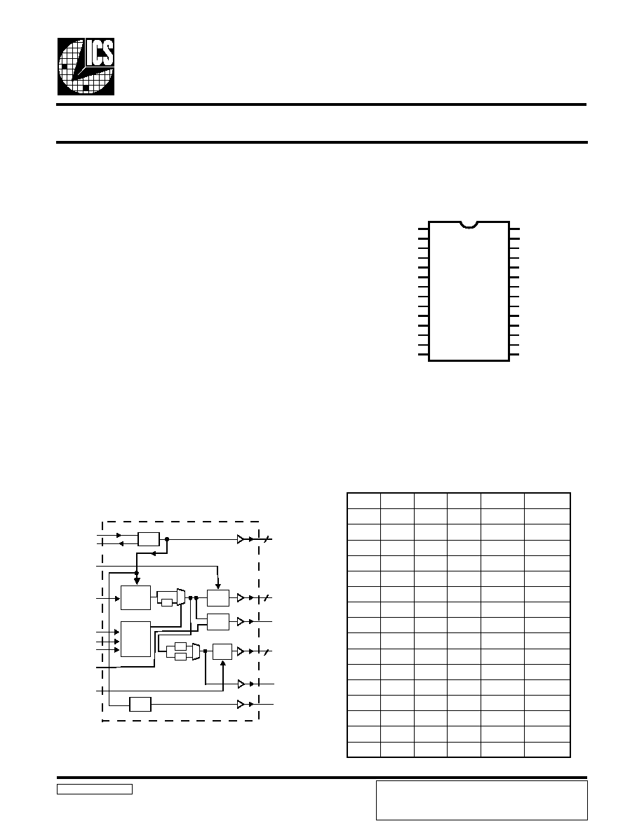
Block Diagram
9248-157 Rev A - 1/16/01
Functionality
Pin Configuration
28 Pin 209mil SSOP
Recommended Application:
ALI1621/1632M style chipsets
Output Features:
·
2 - CPUs @2.5V, up to 140MHz.
·
7 - PCI @3.3V, (including one free running)
·
1 - 48MHz, @3.3V fixed.
·
2 - REF @3.3V, 14.318MHz.
Features:
·
Up to 140 MHz frequency support
·
Support power management: CPU, PCI stop and
Power down.
·
Spread spectrum for EMI control (0.5% down spread).
·
Uses external 14.318MHz crystal
·
FS pins for frequency select
Key Specifications:
·
CPU CPU: <175ps
·
PCI PCI: <250ps
·
CPU(early)-PCI: 1.5ns - 4ns
·
PCI_E (early) - PCI: 2.1ns
Frequency Timing Generator for Pentium II Systems
FS (3:0)
CPU_STOP#
X1
X2
OSC
PLL
Spread
Spectrum
Glitch
Free
Control
Logic
REF (1:0)
2
5
PCICLK (4:0),
PCICLK_E
48MHz
PCI_STOP#
SEL_CPUF#
PD#
Div4#
/ 4
BUS
STOP
PCICLK_F
PLL2
2
CPUCLK 1
CPUCLK0/F
CPU
STOP
CPU
STOP
/ 2
/ 3
SPREAD#
3
S
F
2
S
F
1
S
F
0
S
F
U
P
C
I
C
P
0
0
0
0
3
3
.
3
3
6
6
.
6
1
0
0
0
1
3
3
.
3
6
6
6
.
1
3
0
0
1
0
9
9
.
9
6
0
0
.
5
3
0
0
1
1
6
6
.
6
6
3
3
.
3
3
0
1
0
0
0
0
.
7
9
3
3
.
2
3
0
1
0
1
2
2
.
6
9
7
0
.
2
3
0
1
1
0
0
5
.
1
9
0
5
.
0
3
0
1
1
1
3
3
.
3
8
7
7
.
7
2
1
0
0
0
0
0
.
0
5
6
6
.
6
1
1
0
0
1
5
2
.
5
9
5
7
.
1
3
1
0
1
0
0
0
.
5
0
1
0
0
.
5
3
1
0
1
1
0
0
.
0
0
1
3
3
.
3
3
1
1
0
0
6
6
.
6
6
6
6
.
6
1
1
1
0
1
5
3
.
6
2
1
6
6
.
1
3
1
1
1
0
5
6
.
9
3
1
0
0
.
5
3
1
1
1
1
3
3
.
3
3
1
3
3
.
3
3
*These inputs have a 120K pull up to VDD
**These inputs have a 120K pull down to GND
*FS1/REF0
X1
X2
**FS2/PCICLK_F
*SEL_CPUF#/PCICLK0
PCICLK1
GND
VDDPCI
PCICLK2
PCICLK3
PCICLK4
PCICLK_E
VDD48
*FS3/48MHz
VDDR
REF1/FS0*
SPREAD#
VDDL
CPUCLK1
CPUCLK0/F
GNDL
GND
PCI_STOP#
VDDA
CPU_STOP#
PD#
DIV/4#
GND
ICS9248-157
1
2
3
4
5
6
7
8
9
10
11
12
13
14
28
27
26
25
24
23
22
21
20
19
18
17
16
15
ICS reserves the right to make changes in the device data
identified in this publication without further notice. ICS advises
its customers to obtain the latest version of all device data to
verify that any information being relied upon by the customer is
2
ICS9248-157
Advance Information
Third party brands and names are the property of their respective owners.
Pin Descriptions
General Description
The ICS9248-157 is the Main clock solution for Notebook designs using the Intel ALI1621/1632M style chipset. Along with
an SDRAM buffer such as the ICS9179-03, it provides all necessary clock signals for such a system.
Spread spectrum may be enabled by driving pin 26, SPREAD# active (Low) at power-on. Spread spectrum typically reduces
system EMI by 8dB to 10dB. This simplifies EMI qualification without resorting to board design iterations or costly shielding.
The ICS9248-157 employs a proprietary closed loop design, which tightly controls the percentage of spreading over process
and temperature variations.
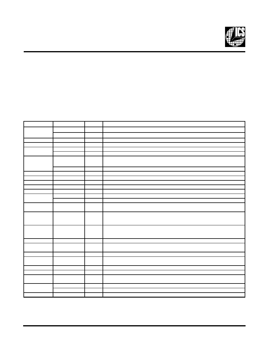
Pin number
Pin name
Type
Description
FS1
Input
Frequency select pin
REF0
Output
3.3V, 14.318 MHz reference clock output.
2
X1
Input
14.318 MHz crystal input
3
X2
Output
14.318 MHz crystal output
FS2
Input
Frequency select pin
PCICLK_F
Output
3.3 V free running PCI clock output, will not be stopped by the PCI_STOP#
SEL_CPUF#
Input
Active low input to select CPUCLK0/F (pin 23) either normal CPUCLK or Free
running (not stoppable through CPU_STOP#) clock.
PCICLK0
Output
3.3V PCI clock output
11, 10, 9, 6
PCICLK (4:1)
Output
3.3 V PCI clock outputs, generating timing requirements
7, 15, 21
GND
Power
Ground for clock outputs
8
VDDPCI
Power
3.3 V power for the PCI clock outputs
12
PCICLK_E
Output
Early PCICLK output, offset from other PCICLKs, stopped by PCI-STOP#
13
VDD48
Power
3.3 V power for 48 MHz clocks
FS3
Input
Frequency select pin
48MHz
Output
Fixed 48MHz clock.
16
DIV4#
Input
Active low input, enables the CPUCLK and the PCICLK to run at 1/4 of the regular
frequecies
17
PD#
Input
Asynchronous active low input pin used to power down the device into a low power
state. The internal clocks are disabled and the VCO and the crystal are stopped. The
latency of the power down will not be greater than 3ms.
18
CPU_STOP#
Input
Asynchronous active low input pin used to stop the CPUCLK in active low state, all
other clocks will continue to run. The CPUCLK will have a "Turnon " latency of at
least 3 CPU clocks.
19
VDDA
Power
3.3 V power for the core
20
PCI-STOP#
Input
Synchronous active low input used to stop the PCICLK in active low state. It will not
effect PCICLK_F or any other outputs.
22
GNDL
Power
Ground for the CPU and Host clock outputs
23
CPUCLK0/F
Output
2.5V CPU clock output; can be selected to be free running by driving
SEL_CPUF# low
24
CPUCLK1
0utput
2.5 V CPU and Host clock outputs
25
VDDL
Power
2.5 V power for the CPU and Host clock outputs
26
SPREAD#
Input
power-on spread spectrum enable option. Active low = spread spectrum clocking
enable. Active high = spread spectrum clocking disable.
FS0
Input
Frequency select pin
REF1
Output
3.3V, 14.318 MHz reference clock output.
28
VDDR
Power
3.3 V power for the REFCLK and crystal clock outputs
14
1
27
4
5
3
ICS9248-157
Third party brands and names are the property of their respective owners.
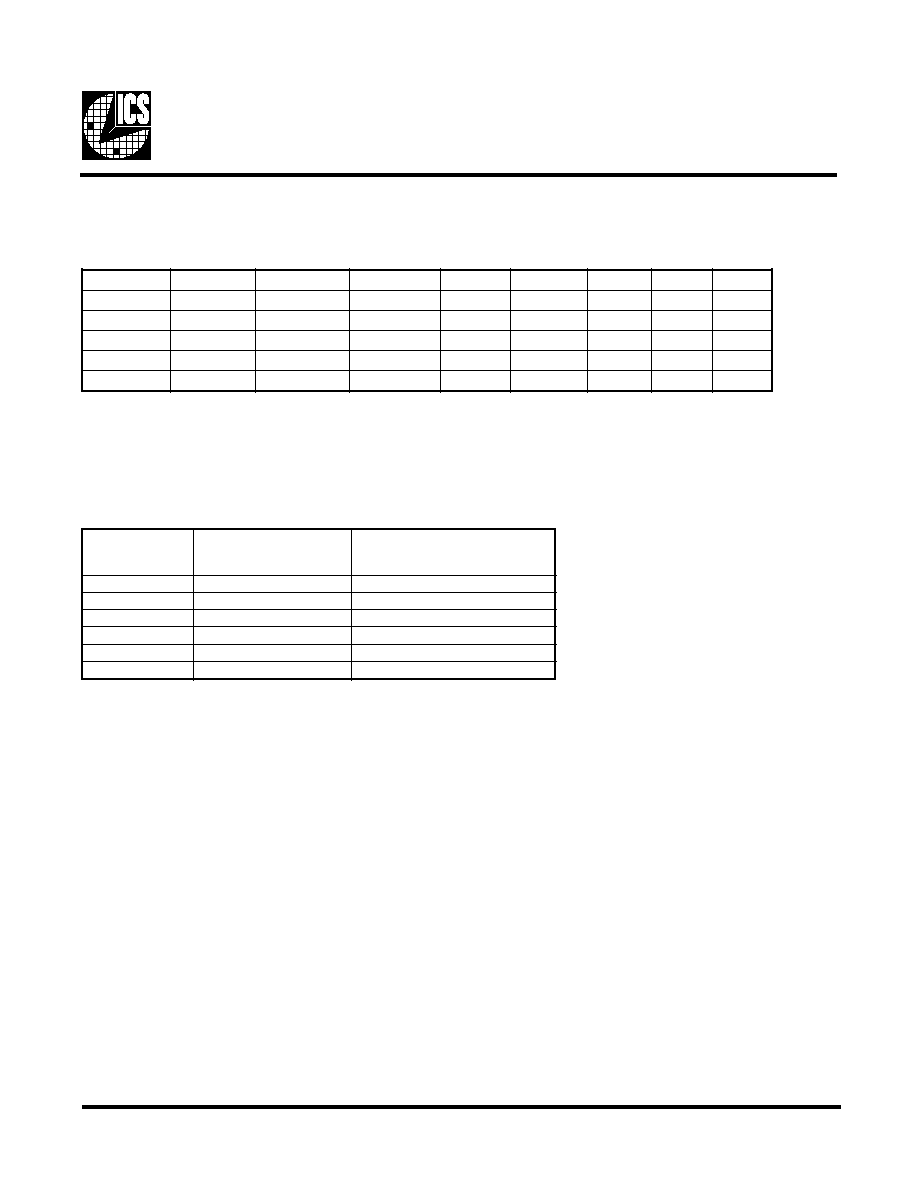
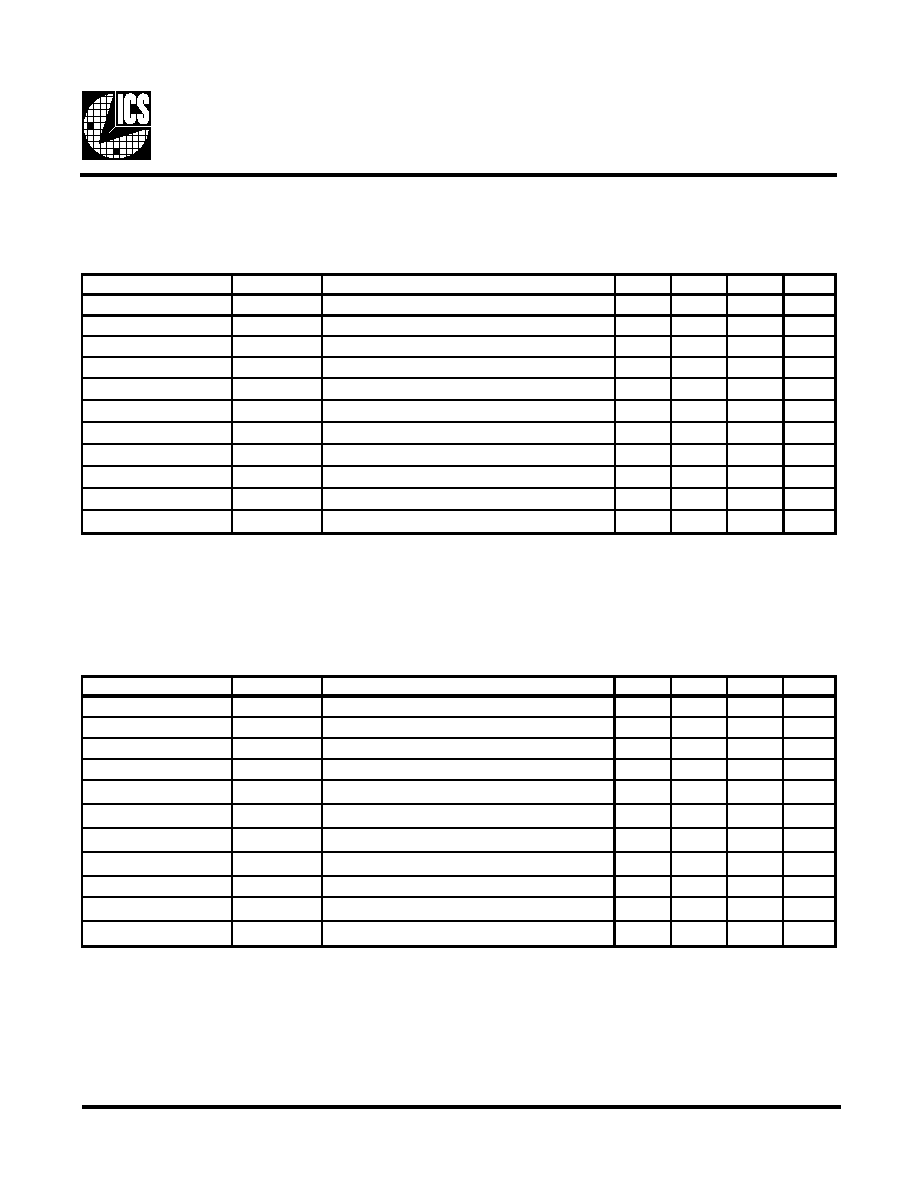
Power Management
Power Management Requirements
Clock Enable Configuration
Full clock cycle timing is guaranteed at all times after the system has initially powered up except where noted. During power up
and power down operations using the PD# pin will not cause clocks of a short or longer pulse than that of the running clock.
The first clock pulse coming out of a stopped clock condition may be slightly distorted due to clock network charging circuitry.
Board routing and signal loading may have a large impact on the initial clock distortion also.
Notes.
1. Clock on latency is defined from when the clock enable goes active to when the first valid clock comes out of the device.
2. Clock off latency is defined from when the clock enable goes inactive to when the last clock is driven low out of the device.
3. Power up latency is when PD# goes inactive (high) to when the first valid clocks are output by the device.
4. Power down has controlled clock counts applicable to CPUCLK, PCICLK only.
The REF will be stopped independant of these.
L
A
N
G
I
S
E
T
A
T
S
L
A
N
G
I
S
y
c
n
e
t
a
L
g
n
i
n
n
u
r
e
e
r
f
f
o
s
e
g
d
e
g
n
i
s
i
r
f
o
.
o
N
K
L
C
I
C
P
#
P
O
T
S
_
U
P
C
)
d
e
l
b
a
s
i
D
(
0
2
1
)
d
e
l
b
a
n
E
(
1
1
1
#
P
O
T
S
_
I
C
P
)
d
e
l
b
a
s
i
D
(
0
2
1
)
d
e
l
b
a
n
E
(
1
1
1
#
D
P
)
n
o
i
t
a
r
e
p
O
l
a
m
r
o
N
(
1
3
s
m
3
)
n
w
o
D
r
e
w
o
P
(
0
4
x
a
m
2
#
P
O
T
S
_
U
P
C
#
P
O
T
S
_
I
C
P
#
N
W
D
_
R
W
P
K
L
C
U
P
C
K
L
C
I
C
P
F
_
K
L
C
I
C
P
F
E
R
l
a
t
s
y
r
C
s
O
C
V
X
X
0
w
o
L
w
o
L
w
o
L
d
e
p
p
o
t
S
f
f
O
f
f
O
0
0
1
w
o
L
w
o
L
g
n
i
n
n
u
R
g
n
i
n
n
u
R
g
n
i
n
n
u
R
g
n
i
n
n
u
R
0
1
1
w
o
L
g
n
i
n
n
u
R
g
n
i
n
n
u
R
g
n
i
n
n
u
R
g
n
i
n
n
u
R
g
n
i
n
n
u
R
1
0
1
g
n
i
n
n
u
R
w
o
L
g
n
i
n
n
u
R
g
n
i
n
n
u
R
g
n
i
n
n
u
R
g
n
i
n
n
u
R
1
1
1
g
n
i
n
n
u
R
g
n
i
n
n
u
R
g
n
i
n
n
u
R
g
n
i
n
n
u
R
g
n
i
n
n
u
R
g
n
i
n
n
u
R
Power Groups:
VDDA = PLL Core
VDD48 = 48MHz Core
VDDPCI = PCICLK
VDDL = CPUCLK
VDDR = Xtal & REF
4
ICS9248-157
Advance Information
Third party brands and names are the property of their respective owners.
Absolute Maximum Ratings
Supply Voltage . . . . . . . . . . . . . . . . . . . . . . . . . . . . 5.5 V
Logic Inputs . . . . . . . . . . . . . . . . . . . . . . . . . . . . . . GND 0.5 V to V
DD
+0.5 V
Ambient Operating Temperature . . . . . . . . . . . . . 0°C to +70°C
Storage Temperature . . . . . . . . . . . . . . . . . . . . . . . 65°C to +150°C
Stresses above those listed under Absolute Maximum Ratings may cause permanent damage to the device. These ratings are
stress specifications only and functional operation of the device at these or any other conditions above those listed in the
operational sections of the specifications is not implied. Exposure to absolute maximum rating conditions for extended periods
may affect product reliability.
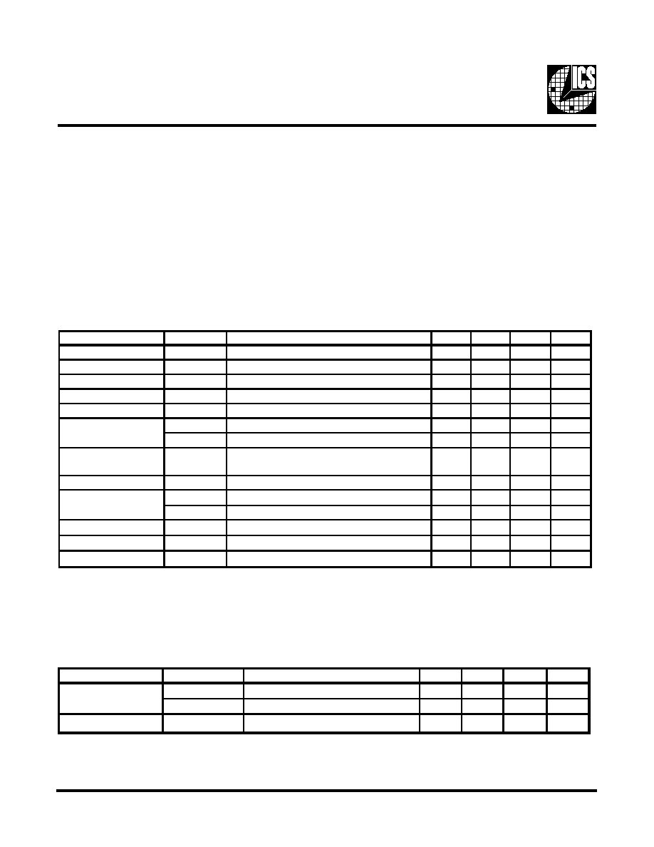
Electrical Characteristics - Input/Supply/Common Output Parameters
T
A
= 0 - 70C; Supply Voltage V
DD
= 3.3 V +/-5% VDDL = 2.5 V +/-5% (unless otherwise stated)
PARAMETER
SYMBOL
CONDITIONS
MIN
TYP
MAX
UNITS
Input High Voltage
V
IH
2
V
DD
+0.3
V
Input Low Voltage
V
IL
V
SS
-0.3
0.8
V
Input High Current
I
IH
V
IN
= V
DD
0.1
5
µA
Input Low Current
I
IL1
V
IN
= 0 V; Inputs with no pull-up resistors
-5
2.0
µA
Input Low Current
I
IL2
V
IN
= 0 V; Inputs with pull-up resistors
-200
-100
µA
Operating
I
DD3.3OP66
C
L
= 0 pF; Select @ 66MHz
60
180
mA
Supply Current
I
DD3.3OP100
C
L
= 0 pF; Select @ 100MHz
66
180
mA
Power Down
I
DD3.3PD
C
L
= 0 pF; With input address to Vdd or GND
70
600
µA
Supply Current
Input frequency
F
i
V
DD
= 3.3 V;
11
14.318
16
MHz
Input Capacitance
1
C
IN
Logic Inputs
5
pF
C
INX
X1 & X2 pins
27
36
45
pF
Transition Time
1
T
trans
To 1st crossing of target Freq.
3
ms
Clk Stabilization
1
T
STAB
From V
DD
= 3.3 V to 1% target Freq.
3
ms
Skew
1
T
CPU-PCI1
V
T
= 1.5 V;
1.5
2.3
4
ns
1
Guaranteed by design, not 100% tested in production.
Electrical Characteristics - Input/Supply/Common Output Parameters
T
A
= 0 - 70C; Supply Voltage V
DD
= 3.3 V +/-5%, V
DDL
= 2.5 V +/-5% (unless otherwise stated)
PARAMETER
SYMBOL
CONDITIONS
MIN
TYP
MAX
UNITS
Operating
I
DD2.5OP66
C
L
= 0 pF; Select @ 66.8 MHz
16
72
mA
Supply Current
I
DD2.5OP100
C
L
= 0 pF; Select @ 100 MHz
23
100
mA
Skew
1
t
CPU-PCI2
V
T
= 1.5 V; V
TL
= 1.25 V
1.5
3
4
ns
1
Guaranteed by design, not 100% tested in production.
5
ICS9248-157
Third party brands and names are the property of their respective owners.
Electrical Characteristics - CPUCLK
T
A
= 0 - 70C; V
DD
= 3.3 V +/-5%, V
DDL
= 2.5 V +/-5%; C
L
= 10 - 20 pF (unless otherwise stated)
PARAMETER
SYMBOL
CONDITIONS
MIN
TYP
MAX
UNITS
Output High Voltage
V
OH2B
I
OH
= -12.0 mA
2
2.3
V
Output Low Voltage
V
OL2B
I
OL
= 12 mA
0.2
0.4
V
Output High Current
I
OH2B
V
OH
= 1.7 V
-41
-19
mA
Output Low Current
I
OL2B
V
OL
= 0.7 V
19
37
mA
Rise Time
t
r2B
1
V
OL
= 0.4 V, V
OH
= 2.0 V
0.99
1.6
ns
Fall Time
t
f2B
1
V
OH
= 2.0 V, V
OL
= 0.4 V
1.05
1.6
ns
Duty Cycle
d
t2B
1
V
T
= 1.25 V
45
50.3
55
%
Skew
t
sk2B
1
V
T
= 1.25 V
34
175
ps
Jitter, Cycle-to-cycle
t
jcyc-cyc2B
1
V
T
= 1.25 V
203
250
ps
Jitter, One Sigma
t
j1s2B
1
V
T
= 1.25 V
150
ps
Jitter, Absolute
t
jabs2B
1
V
T
= 1.25 V
-250
+250
ps
1
Guaranteed by design, not 100% tested in production.
Electrical Characteristics - PCICLK
T
A
= 0 - 70C; V
DD
= 3.3 V +/-5% VDDL = 2.5 V +/-5%; C
L
= 30 pF
PARAMETER
SYMBOL
CONDITIONS
MIN
TYP
MAX UNITS
Output High Voltage
V
OH1
I
OH
= -11 mA
2.4
3.1
V
Output Low Voltage
V
OL1
I
OL
= 9.4 mA
0.1
0.4
V
Output High Current
I
OH1
V
OH
= 2.0 V
-62
-22
mA
Output Low Current
I
OL1
V
OL
= 0.8 V
16
57
mA
Rise Time
1
t
r1
V
OL
= 0.4 V, V
OH
= 2.4 V
1.5
2
ns
Fall Time
1
t
f1
V
OH
= 2.4 V, V
OL
= 0.4 V
1.1
2
ns
Duty Cycle
1
d
t1
V
T
= 1.5 V
45
50
55
%
Skew
1
t
sk1
V
T
= 1.5 V
290
500
ps
Jitter, Cycle-to-cycle
t
jcyc-cyc1
V
T
= 1.25 V
200
500
ps
Jitter, One Sigma
1
t
j1s1
V
T
= 1.5 V
150
ps
Jitter, Absolute
1
t
jabs1
V
T
= 1.5 V
-250
250
ps
1
Guaranteed by design, not 100% tested in production.