9248-179
ICS9248-179
Third party brands and names are the property of their respective owners.
Integrated
Circuit
Systems, Inc.
9248-179 Rev B 08/22/01
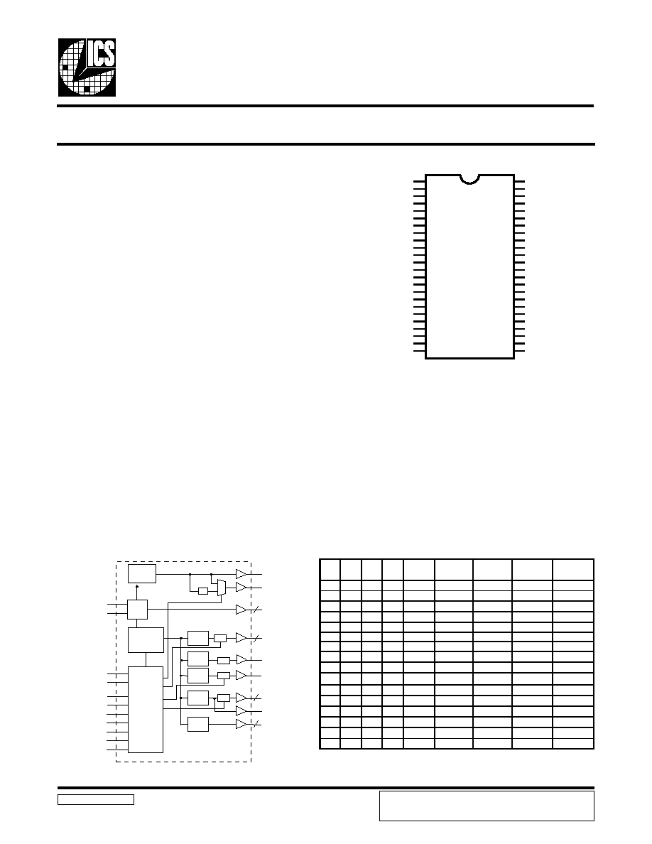
Frequency Generator for Intel Pentium III Celeron Processor
Block Diagram
Recommended Application:
Single chip clock solution for SIS 635/640 Intel Pentium III
Celeron chipset.
Output Features:
·
2 - CPUs @ 2.5V.
·
1 - IOAPIC @ 2.5V.
·
1 - SDRAM @ 3.3V
·
6- PCI @3.3V
·
2 - AGP @ 3.3V
·
1- 48MHz, @3.3V fixed.
·
1- 24/48MHz, @3.3V selectable by I
2
C
(Default is 24MHz)
·
2- REF @3.3V, 14.318MHz.
Features:
·
Up to 166MHz frequency support
·
Support FS0-FS3 trapping status bit for I
2
C read back.
·
Support power management: CPU, PCI, SDRAM stop
and Power down Mode from I
2
C programming.
·
Spread spectrum for EMI control (0 to -0.5%, ± 0.25%).
·
Uses external 14.318MHz crystal
Skew Specifications:
·
CPU - CPU: < 175ps
·
PCI - PCI: < 500ps
·
CPU - SDRAM: < 250ps
·
CPU (early) - PCI: 1-4ns (typ. 2ns)
·
AGP - AGP: <175ps
·
CPU - AGP: 1-4ns
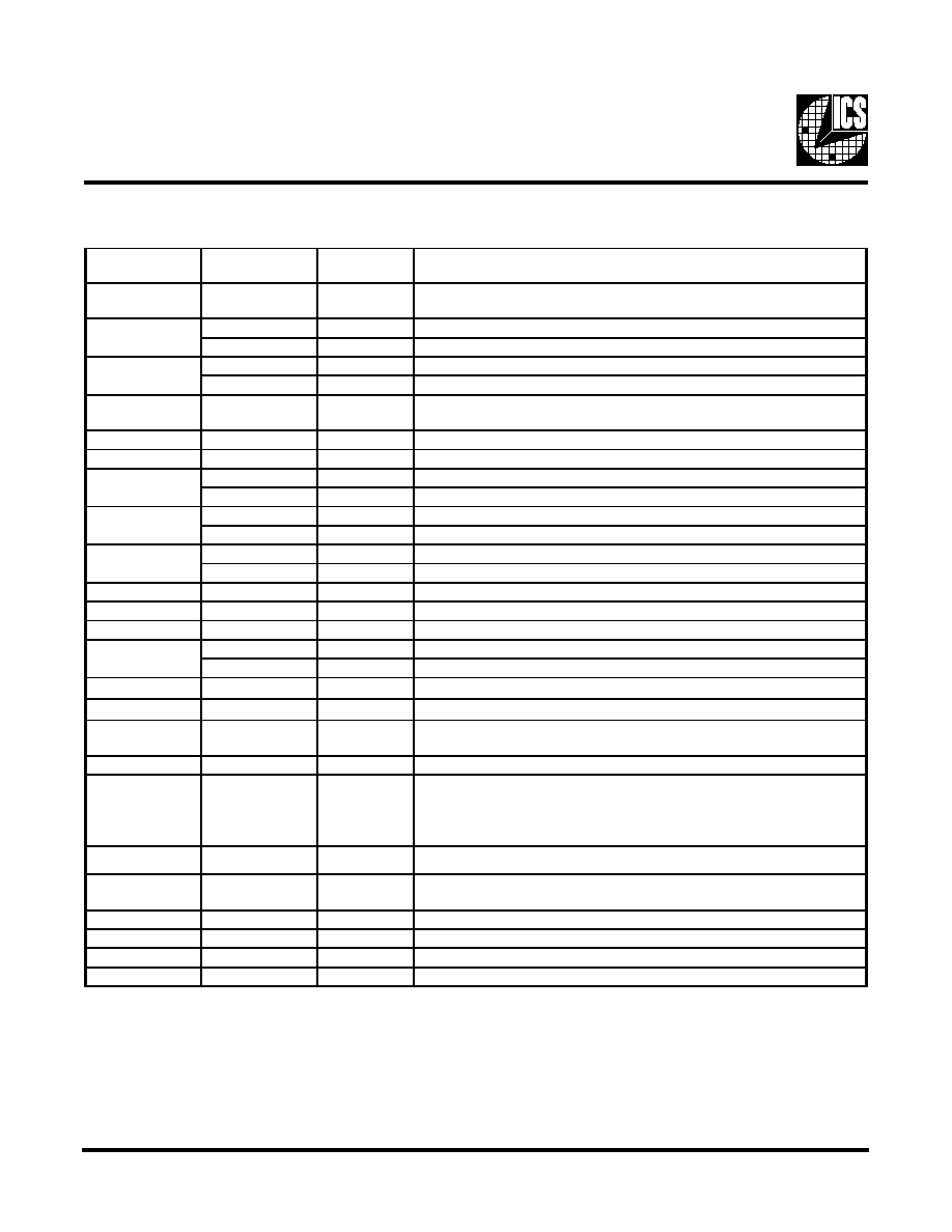
Functionality
Pin Configuration
48-Pin 300mil SSOP
* These are double strength.
** (1X/2X) have single or double strength to
drive 2 loads.
1. Internal pull-up, of 120K to V
DD
.
2. These inputs have a 120K pull down to GND.
VDDREF
REF0
*FS1/REF1
GND
GND
X1
X2
GND
VDDPCI
PCICLK1
PCICLK2
GND
PCICLK3
PCICLK4
VDDAGP
AGPCLK0
AGPCLK1
GND
VDD48
48MHz
AGPSEL/ 24_48MHz
GND
2
2
*FS0/
2
2
2
1
FS2/PCICLK_F
FS3/PCICLK0
**FS4/
**
**
**
2
VDDLAPIC
IOAPIC*
GND
VDDL
CPUCLK0
NC
GND
VDDL
CPUCLK1
GND
NC
NC
VDDSDR
SDRAM
GND
PCI_STOP#
CPU_STOP#
PD#
SDRAM_STOP#
AGP_STOP#
SDATA
SCLK
GND
VDD
2
2
1
2
2
ICS9248-179
1
2
3
4
5
6
7
8
9
10
11
12
13
14
15
16
17
18
19
20
21
22
23
24
48
47
46
45
44
43
42
41
40
39
38
37
36
35
34
33
32
31
30
29
28
27
26
25
PLL2
PLL1
Spread
Spectrum
48MHz
24_48MHz
CPUCLK (1:0)
SDRAM
PCICLK (4:0)
AGP (1:0)
IOAPIC
PCICLK_F
2
5
2
2
X1
X2
XTAL
OSC
CPU
DIVDER
SDRAM
DIVDER
PCI
DIVDER
Stop
Stop
Stop
SDATA
SCLK
FS (4:0)
PD#
PCI_STOP#
CPU_STOP#
SDRAM_STOP#
AGP_STOP#
AGP_SEL
Control
Logic
Config.
Reg.
/ 2
REF (1:0)
AGP
DIVDER
Stop
IOAPIC
DIVDER
Preliminary Product Preview
PRODUCT PREVIEW documents contain information on new
products in the sampling or preproduction phase of development.
Characteristic data and other specifications are subject to change
without notice.
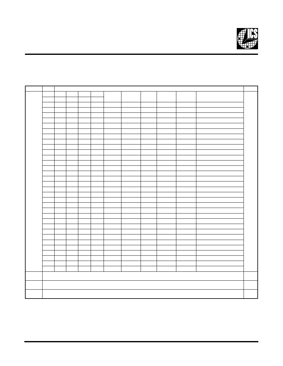
0
0
0
0
66.66
66.66
33.33
66.66
50
0
0
0
1
100
100
33.33
66.66
50
0
0
1
0
166.66 166.66
33.33
66.66
55.6
0
0
1
1
133.33 133.33
33.33
66.66
50
0
1
0
0
66.66
100
33.33
66.66
50
0
1
0
1
100
66.66
33.33
66.66
50
0
1
1
0
100
133.33
33.33
66.66
50
0
1
1
1
133.33
100
33.33
66.66
50
1
0
0
0
112
112
33.6
67.2
56
1
0
0
1
124
124
31
62
46.5
1
0
1
0
138
138
34.5
69
46.0
1
0
1
1
150
150
30
60
50
1
1
0
0
66.66
133.33
33.33
66.66
49.84
1
1
0
1
133.33 166.66
33.33
66.66
55.3
1
1
1
0
150
100
30
60
50
1
1
1
1
160
120
30
60
48
AGP SEL
= 0
AGP SEL
= 1
PCICLK
FS3 FS2 FS1 FS0 CPU
SDRAM
Note: Please see full table on page 4.
2
ICS9248-179
Preliminary Product Preview
Third party brands and names are the property of their respective owners.
Pin Configuration
PIN N UMBER
PIN NA ME
TY PE
DESCR IPTION
1, 11, 17, 21,
25, 36
V DD
PWR
3.3V Power supply for SD RAM output buffers, PCI output buffers,
reference output buffers and 48M H z output.
FS0
IN
Frequency select pin.
REF0
O UT
14.318 M H z reference clock.
FS1
IN
Frequency select pin.
REF1
O UT
14.318 M H z reference clock.
4, 5, 8, 14, 20, 24,
26, 34, 39, 42, 46
G ND
PWR
G round pin for outputs.
6
X 1
IN
Crystal input,nominally 14.318M Hz.
7
X 2
O UT
Crystal output, nominally 14.318M H z.
FS2
IN
Frequency select pin.
PCICLK_F
O UT
PCI clock output, not affected by PCI_STOP#.
FS3
IN
Frequency select pin.
PCICLK0
O UT
PCI clock output.
FS4
IN
Frequency select pin.
PCICLK1
O UT
PCI clock output.
16, 15, 13
PCICLK (4:2)
O UT
PCI clock outputs.
19, 18
AGPCLK (1:0)
O UT
A GP outputs defined as 2X PCI. These may not be stopped.
22
48M H z
O UT
48M Hz output clock.
AG PSEL
IN
A GP frequency select pin.
24_48M Hz
O UT
Clock output for super I/O/USB default is 24M Hz.
27
SCLK
IN
Clock pin of I
2
C circuitry 5V tolerant.
28
SD ATA
I/O
D ata pin for I
2
C circuitry 5V tolerant.
29
AGP_STOP#
IN
Stops all AG P clocks besides the AG P_F clocks at logic 0 level,
w hen input low .
30
SD RA M _STO P#
IN
Stops all SD RAM clocks at logic 0 level, when input low .
31
PD#
IN
A synchronous active low input pin used to pow er down the device into a low
pow er state. The internal clocks are disabled and the V CO and the crystal are
stopped. The latency of the power dow n w ill not be greater than 3ms.
32
CPU_STO P#
IN
Stops all CPU CLKs clocks at logic 0 level, when input low
33
PCI_STO P#
IN
Stops all PCICLKs besides the PCICLK_F clocks at logic 0 level,
w hen input low .
35
SD RAM
O UT
SDRAM clock output.
37, 38, 43
NC
-
N o connect pins.
40, 44
CPUCLK (1:0)
O UT
CPU clock outputs.
41, 45, 48
V DD L
PWR
Supply for CPU and IOA PIC clocks at 2.5V nominal.
2
9
10
23
3
12

3
ICS9248-179
Preliminary Product Preview
Third party brands and names are the property of their respective owners.
The ICS9248-179 is the single chip clock solution for Desktop/Notebook designs using the SIS 635/640 style chipset. It
provides all necessary clock signals for such a system.
Spread spectrum may be enabled through I
2
C programming. Spread spectrum typically reduces system EMI by 8dB to 10dB.
This simplifies EMI qualification without resorting to board design iterations or costly shielding. The ICS9248-179
employs a proprietary closed loop design, which tightly controls the percentage of spreading over process and temperature
variations.
Serial programming I
2
C interface allows changing functions, stop clock programming and frequency selection.
General Description
Power Groups
VDDCPU = CPU
VDDPCI = PCICLK_F, PCICLK
VDDSDR = SDRAM
VDD48 = 48MHz, 24MHz, fixed PLL
VDDA = Core, PLL, X1, X2
VDDAGP=AGP, REF
4
ICS9248-179
Preliminary Product Preview
Third party brands and names are the property of their respective owners.
Serial Configuration Command Bitmap
Note: PWD = Power-Up Default
I
2
C is a trademark of Philips Corporation
Note1:
Default at power-up will be for latched logic inputs to define frequency, as displayed by Bit 3.
Byte4: Functionality and Frequency Select Register (default = 0)
Bytes 0-3: Are reserved for external clock buffer.
t
i
B
n
o
i
t
p
i
r
c
s
e
D
D
W
P
2
t
i
B
4
:
7
t
i
B
2
t
i
B
7
t
i
B
6
t
i
B
5
t
i
B
4
t
i
B
U
P
C
M
A
R
D
S
I
C
P
P
G
A
0
=
L
E
S
P
G
A
1
=
L
E
S
e
g
a
t
n
e
c
e
r
P
d
a
e
r
p
S
0
0
0
0
0
1
e
t
o
N
4
S
F
3
S
F
2
S
F
1
S
F
0
S
F
0
0
0
0
0
6
6
.
6
6
6
6
.
6
6
3
3
.
3
3
6
6
.
6
6
0
5
d
a
e
r
p
S
n
w
o
D
%
5
.
0
-
o
t
0
0
0
0
0
1
0
0
1
0
0
1
3
3
.
3
3
6
6
.
6
6
0
5
d
a
e
r
p
S
n
w
o
D
%
5
.
0
-
o
t
0
0
0
0
1
0
6
6
.
6
6
1
6
6
.
6
6
1
3
3
.
3
3
6
6
.
6
6
6
.
5
5
d
a
e
r
p
S
r
e
t
n
e
C
%
5
2
.
0
-
/
+
0
0
0
1
1
3
3
.
3
3
1
3
3
.
3
3
1
3
3
.
3
3
6
6
.
6
6
0
5
d
a
e
r
p
S
n
w
o
D
%
5
.
0
-
o
t
0
0
0
1
0
0
6
6
.
6
6
0
0
1
3
3
.
3
3
6
6
.
6
6
0
5
d
a
e
r
p
S
n
w
o
D
%
5
.
0
-
o
t
0
0
0
1
0
1
0
0
1
6
6
.
6
6
3
3
.
3
3
6
6
.
6
6
0
5
d
a
e
r
p
S
n
w
o
D
%
5
.
0
-
o
t
0
0
0
1
1
0
0
0
1
3
3
.
3
3
1
3
3
.
3
3
6
6
.
6
6
0
5
d
a
e
r
p
S
n
w
o
D
%
5
.
0
-
o
t
0
0
0
1
1
1
3
3
.
3
3
1
0
0
1
3
3
.
3
3
6
6
.
6
6
0
5
d
a
e
r
p
S
n
w
o
D
%
5
.
0
-
o
t
0
0
1
0
0
0
2
1
1
2
1
1
6
.
3
3
2
.
7
6
6
5
d
a
e
r
p
S
r
e
t
n
e
C
%
5
2
.
0
-
/
+
0
1
0
0
1
4
2
1
4
2
1
1
3
2
6
5
.
6
4
d
a
e
r
p
S
r
e
t
n
e
C
%
5
2
.
0
-
/
+
0
1
0
1
0
8
3
1
8
3
1
5
.
4
3
9
6
0
.
6
4
d
a
e
r
p
S
r
e
t
n
e
C
%
5
2
.
0
-
/
+
0
1
0
1
1
0
5
1
0
5
1
0
3
0
6
0
5
d
a
e
r
p
S
r
e
t
n
e
C
%
5
2
.
0
-
/
+
0
1
1
0
0
6
6
.
6
6
3
3
.
3
3
1
3
3
.
3
3
6
6
.
6
6
4
8
.
9
4
d
a
e
r
p
S
n
w
o
D
%
5
.
0
-
o
t
0
0
1
1
0
1
3
3
.
3
3
1
6
6
.
6
6
1
3
3
.
3
3
6
6
.
6
6
3
.
5
5
d
a
e
r
p
S
n
w
o
D
%
5
.
0
-
o
t
0
0
1
1
1
0
0
5
1
0
0
1
0
3
0
6
0
5
d
a
e
r
p
S
r
e
t
n
e
C
%
5
2
.
0
-
/
+
0
1
1
1
1
0
6
1
0
2
1
0
3
0
6
8
4
d
a
e
r
p
S
r
e
t
n
e
C
%
5
2
.
0
-
/
+
1
0
0
0
0
0
9
0
9
0
3
0
6
5
4
d
a
e
r
p
S
r
e
t
n
e
C
%
5
2
.
0
-
/
+
1
0
0
0
1
9
.
0
0
1
9
.
0
0
1
3
6
.
3
3
7
2
.
7
6
5
4
.
0
5
d
a
e
r
p
S
r
e
t
n
e
C
%
5
2
.
0
-
/
+
1
0
0
1
0
3
0
1
3
0
1
3
3
.
4
3
7
6
.
8
6
5
.
1
5
d
a
e
r
p
S
r
e
t
n
e
C
%
5
2
.
0
-
/
+
1
0
0
1
1
9
.
3
3
1
9
.
3
3
1
8
4
.
3
3
7
6
.
8
6
6
5
.
1
5
d
a
e
r
p
S
r
e
t
n
e
C
%
5
2
.
0
-
/
+
1
0
1
0
0
3
3
.
7
3
1
3
0
1
3
3
.
4
3
5
9
.
6
6
5
4
.
1
5
d
a
e
r
p
S
r
e
t
n
e
C
%
5
2
.
0
-
/
+
1
0
1
0
1
3
3
.
7
3
1
3
3
.
7
3
1
3
3
.
4
3
7
6
.
8
6
1
2
.
0
5
d
a
e
r
p
S
r
e
t
n
e
C
%
5
2
.
0
-
/
+
1
0
1
1
0
9
.
0
0
1
9
.
3
3
1
8
4
.
3
3
5
9
.
6
6
1
2
.
0
5
d
a
e
r
p
S
r
e
t
n
e
C
%
5
2
.
0
-
/
+
1
0
1
1
1
9
.
3
3
1
9
.
0
0
1
8
4
.
3
3
5
9
.
6
6
1
2
.
0
5
d
a
e
r
p
S
r
e
t
n
e
C
%
5
2
.
0
-
/
+
1
1
0
0
0
7
0
1
7
0
1
6
6
.
5
3
3
3
.
1
7
5
.
3
5
d
a
e
r
p
S
r
e
t
n
e
C
%
5
2
.
0
-
/
+
1
1
0
0
1
7
0
1
6
6
.
2
4
1
6
6
.
5
3
3
3
.
1
7
5
.
3
5
d
a
e
r
p
S
r
e
t
n
e
C
%
5
2
.
0
-
/
+
1
1
0
1
0
6
6
.
2
4
1
6
6
.
2
4
1
6
6
.
5
3
3
3
.
1
7
5
.
3
5
d
a
e
r
p
S
r
e
t
n
e
C
%
5
2
.
0
-
/
+
1
1
0
1
1
0
1
1
0
1
1
6
6
.
6
3
3
3
.
3
7
5
5
d
a
e
r
p
S
r
e
t
n
e
C
%
5
2
.
0
-
/
+
1
1
1
0
0
0
1
1
6
6
.
6
4
1
6
6
.
6
3
3
3
.
3
7
5
5
d
a
e
r
p
S
r
e
t
n
e
C
%
5
2
.
0
-
/
+
1
1
1
0
1
6
6
.
6
4
1
6
6
.
6
4
1
6
6
.
6
3
3
3
.
3
7
5
5
d
a
e
r
p
S
r
e
t
n
e
C
%
5
2
.
0
-
/
+
1
1
1
1
0
7
.
6
6
1
5
2
1
5
2
.
1
3
8
6
.
6
6
7
5
.
5
5
d
a
e
r
p
S
r
e
t
n
e
C
%
5
2
.
0
-
/
+
1
1
1
1
1
0
.
0
0
2
0
.
0
0
2
3
3
.
3
3
6
6
.
6
6
0
5
d
a
e
r
p
S
r
e
t
n
e
C
%
5
2
.
0
-
/
+
3
t
i
B
s
t
u
p
n
I
d
e
h
c
t
a
L
,t
c
e
l
e
s
e
r
a
w
d
r
a
h
y
b
d
e
t
c
e
l
e
s
s
i
y
c
n
e
u
q
e
r
F
-
0
4
:
7
2
,
t
i
B
y
b
d
e
t
c
e
l
e
s
s
i
y
c
n
e
u
q
e
r
F
-
1
0
1
t
i
B
l
a
m
r
o
N
-
0
d
e
l
b
a
n
E
m
u
r
t
c
e
p
S
d
a
e
r
p
S
-
1
1
0
t
i
B
g
n
i
n
n
u
R
-
0
s
t
u
p
t
u
o
l
l
a
e
t
a
t
s
i
r
T
-
1
0
5
ICS9248-179
Preliminary Product Preview
Third party brands and names are the property of their respective owners.
Byte 5: CPU, Active/Inactive Register
(1= enable, 0 = disable)
Byte 6: PCI, Active/Inactive Register
(1= enable, 0 = disable)
T
I
B
#
N
I
P
D
W
P
N
O
I
T
P
I
R
C
S
E
D
7
t
i
B
9
1
1
)
e
v
i
t
c
a
n
I
/
t
c
A
(
1
K
L
C
P
G
A
6
t
i
B
8
1
1
)
e
v
i
t
c
a
n
I
/
t
c
A
(
0
K
L
C
P
G
A
5
t
i
B
6
1
1
)
e
v
i
t
c
a
n
I
/
t
c
A
(
4
K
L
C
I
C
P
4
t
i
B
5
1
1
)
e
v
i
t
c
a
n
I
/
t
c
A
(
3
K
L
C
I
C
P
3
t
i
B
3
1
1
)
e
v
i
t
c
a
n
I
/
t
c
A
(
2
K
L
C
I
C
P
2
t
i
B
2
1
1
)
e
v
i
t
c
a
n
I
/
t
c
A
(
1
K
L
C
I
C
P
1
t
i
B
0
1
1
)
e
v
i
t
c
a
n
I
/
t
c
A
(
0
K
L
C
I
C
P
0
t
i
B
3
2
X
)
k
c
a
b
d
a
e
r
(
L
E
S
P
G
A
T
I
B
#
N
I
P
D
W
P
N
O
I
T
P
I
R
C
S
E
D
7
t
i
B
-
0
d
e
v
r
e
s
e
R
6
t
i
B
-
0
d
e
v
r
e
s
e
R
5
t
i
B
-
0
d
e
v
r
e
s
e
R
4
t
i
B
-
0
d
e
v
r
e
s
e
R
3
t
i
B
-
0
d
e
v
r
e
s
e
R
2
t
i
B
-
0
d
e
v
r
e
s
e
R
1
t
i
B
-
0
d
e
v
r
e
s
e
R
0
t
i
B
-
1
d
e
v
r
e
s
e
R
Byte 8: Vendor ID Register
(1= enable, 0 = disable)
Byte 7: Control, Active/Inactive Register
(1= enable, 0 = disable)
T
I
B
#
N
I
P
D
W
P
N
O
I
T
P
I
R
C
S
E
D
7
t
i
B
3
2
1
)
f
f
O
:
0
,
n
O
:
1
(
M
8
4
_
M
4
2
6
t
i
B
3
,
2
0
l
o
r
t
n
o
C
_
X
2
X
1
_
F
E
R
)
x
2
:
1
,
x
1
:
0
(
5
t
i
B
7
4
1
l
o
r
t
n
o
C
_
X
2
X
1
C
I
P
A
)
x
2
:
1
,
x
1
:
0
(
4
t
i
B
3
1
)
e
v
i
t
c
a
n
I
/
t
c
A
(
1
F
E
R
3
t
i
B
2
1
)
e
v
i
t
c
a
n
I
/
t
c
A
(
0
F
E
R
2
t
i
B
-
0
t
c
e
l
e
S
C
I
P
A
O
I
)
z
H
M
3
3
.
3
3
:
1
,
z
H
M
7
6
.
6
1
:
0
(
1
t
i
B
3
2
1
t
c
e
l
e
S
M
8
4
_
M
4
2
)
z
H
M
8
4
:
0
,
z
H
M
4
2
:
1
(
0
t
i
B
2
2
1
)
e
v
i
t
c
a
n
I
/
t
c
A
(
z
H
M
8
4
T
I
B
#
N
I
P
D
W
P
N
O
I
T
P
I
R
C
S
E
D
7
t
i
B
2
1
0
l
o
r
t
n
o
C
_
X
2
X
1
_
1
K
L
C
L
C
P
)
x
1
:
0
,
x
2
:
1
(
6
t
i
B
3
1
0
l
o
r
t
n
o
C
_
X
2
X
1
_
2
K
L
C
L
C
P
)
x
1
:
0
,
x
2
:
1
(
5
t
i
B
0
1
X
)
k
c
a
b
d
a
e
r
(
3
S
F
4
t
i
B
9
X
)
k
c
a
b
d
a
e
r
(
2
S
F
3
t
i
B
3
X
)
k
c
a
b
d
a
e
r
(
1
S
F
2
t
i
B
2
X
)
k
c
a
b
d
a
e
r
(
0
S
F
1
t
i
B
5
1
X
l
o
r
t
n
o
C
_
X
2
X
1
_
3
K
L
C
L
C
P
)
x
1
:
0
,
x
2
:
1
(
0
t
i
B
6
1
X
l
o
r
t
n
o
C
_
X
2
X
1
_
4
K
L
C
L
C
P
)
x
1
:
0
,
x
2
:
1
(