Äîêóìåíòàöèÿ è îïèñàíèÿ www.docs.chipfind.ru
Integrated
Circuit
Systems, Inc.
ICS9248-189
Third party brands and names are the property of their respective owners.
Block Diagram
9248-189 Rev - 08/10/01
Advance Information
ADVANCE INFORMATION documents contain information on products
in the formative or design phase development. Characteristic data and
other specifications are design goals. ICS reserves the right to change or
discontinue these products without notice.
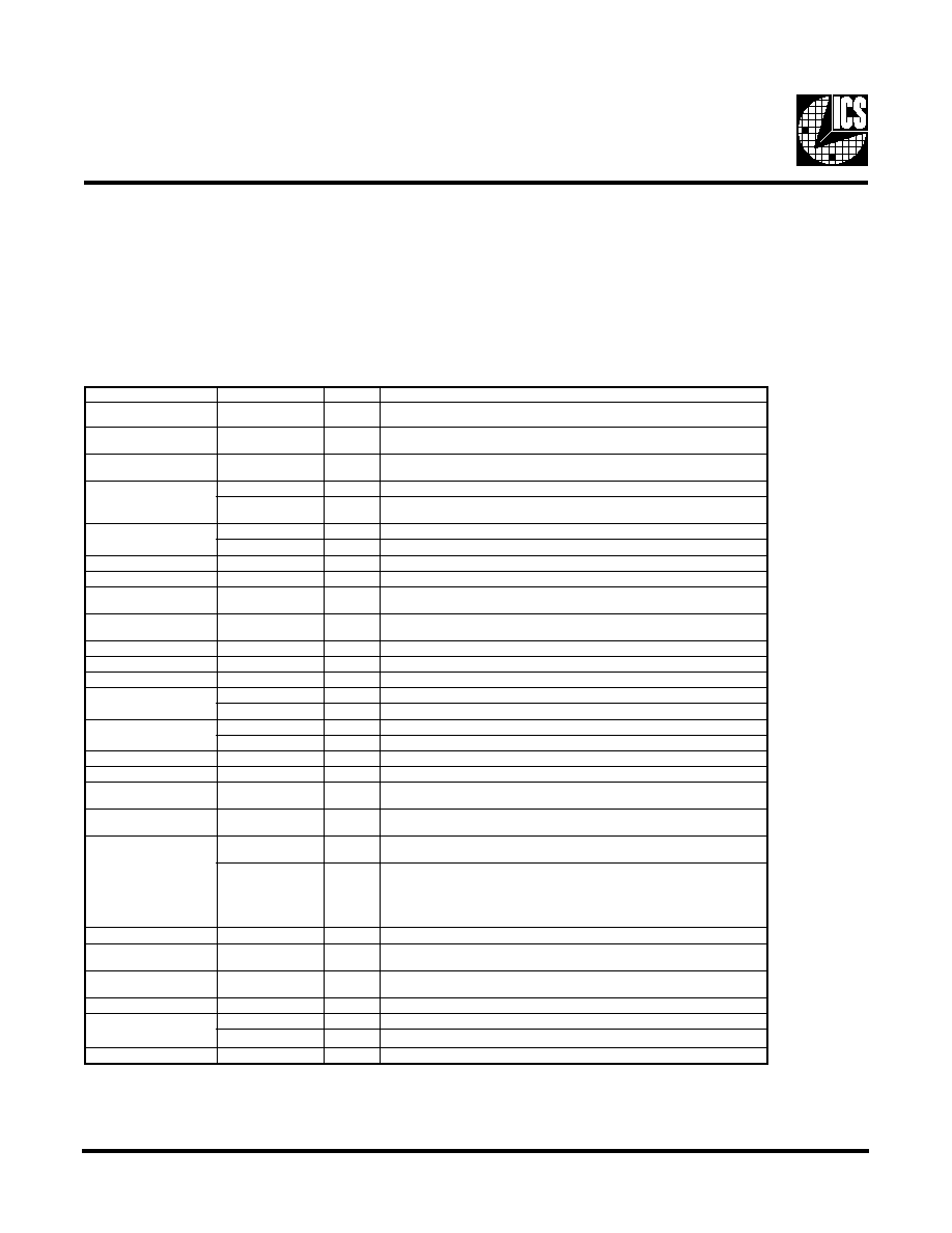
Functionality
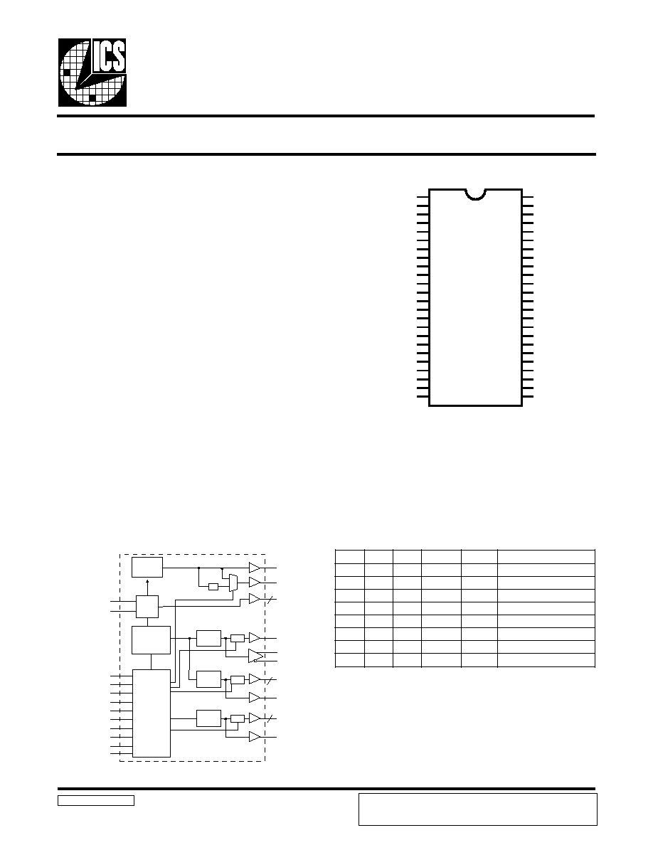
Pin Configuration
48-Pin 300mil SSOP & 240mil TSSOP
Recommended Application:
VIA K7/KN/KX-133 style chipset
Output Features:
·
1 - Differential pair open drain CPU clocks
·
1 - CPU clock @ 3.3V
·
7 - SDRAM @ 3.3V
·
8 - PCI @ 3.3V,
·
1 - 48MHz, @ 3.3V fixed
·
1 - 24/48MHz @ 3.3V
·
3 - REF @ 3.3V, 14.318MHz.
Features:
·
Up to 166MHz frequency support
·
Support power management via hardware select CPU
stop, CLOCK stop, PCI stop, and SDRAM stop
·
Support power management via I
2
C programing
·
Spread spectrum for EMI control
(± 0.25% to ± 0.06% center, or 0 to -0.5% or -1.0% down
spread)
·
Uses external 14.318MHz crystal
Key Specifications:
·
CPU - CPU Skew: <175ps
·
CPU - SDRAM Skew: ±125ps
·
CPU - PCI Skew: ±100ps
·
PCI - PCI Skew: <500ps
AMD - K7
TM
Clock Generator for Mobile System
* Internal Pull-up Resistor of 120K to VDD
1
These outputs have double strength to drive 2 loads.
2
These outputs can be set to 1X or 1.5X strength
through I
2
C
VDDREF
X1
X2
*FS2/PCICLK_F
*FS1/PCICLK0
VDDPCI
GND
PCICLK1
PCICLK2
PCICLK3
PCICLK4
PCICLK5
GND
VDDPCI
PCICLK6
*SDRAM_STOP#
*PCI_STOP#
BUFFER_IN
AVDD
GND
GND
*FS0/48MHZ
*SEL24_48#/24_48MHz
VDD48
REF0
REF
REF2/FS3
GND
GND
VDD
CPUCLK_CS
CPUCLKT0
CPUCLKC0
CPU_STOP#*
CLK_STOP#*/
SDRAM0
SDRAM1
VDDSDR
GND
SDRAM2
SDRAM3
GND
VDDSDR
SDRAM4
SDRAM5
SDRAM_F
SCLK
SDATA
1
2
2
1
*
PD#
ICS9248-189
1
2
3
4
5
6
7
8
9
10
11
12
13
14
15
16
17
18
19
20
21
22
23
24
48
47
46
45
44
43
42
41
40
39
38
37
36
35
34
33
32
31
30
29
28
27
26
25
2
S
F
1
S
F
0
S
F
U
P
C
I
C
P
e
g
a
t
n
e
c
r
e
P
d
a
e
r
p
S
0
0
0
0
0
.
0
0
1
3
3
.
3
3
d
a
e
r
p
S
r
e
t
n
e
C
%
5
3
.
0
-
/
+
0
0
1
3
3
.
3
3
1
3
3
.
3
3
d
a
e
r
p
S
r
e
t
n
e
C
%
5
3
.
0
-
/
+
0
1
0
0
0
.
0
0
1
3
3
.
3
3
d
a
e
r
p
S
n
w
o
D
%
5
.
0
-
o
t
0
0
1
1
3
3
.
3
3
1
3
3
.
3
3
d
a
e
r
p
S
n
w
o
D
%
5
.
0
-
o
t
0
1
0
0
0
0
.
0
0
1
3
3
.
3
3
d
a
e
r
p
S
r
e
t
n
e
C
%
6
.
0
-
/
+
1
0
1
3
3
.
3
3
1
3
3
.
3
3
d
a
e
r
p
S
r
e
t
n
e
C
%
6
.
0
-
/
+
1
1
0
0
0
.
0
0
1
3
3
.
3
3
d
a
e
r
p
S
o
N
1
1
1
3
3
.
3
3
1
3
3
.
3
3
d
a
e
r
p
S
o
N
SEL24_48#
SDATA
SCLK
FS (3:0)
PD#
CPU_STOP#
CLK_STOP#
PCI_STOP#
SDRAM_STOP#
BUFFER_IN
PLL2
PLL1
Spread
Spectrum
48MHz
24_48MHz
SDRAM (5:0)
PCICLK (6:0)
PCICLK_F
SDRAM_F
CPUCLK_CS
X1
X2
XTAL
OSC
CPU
DIVDER
PCI
DIVDER
Stop
Stop
Stop
Control
Logic
Config.
Reg.
/ 2
REF (2:0)
SDRAM
DIVIDER
7
3
6
CPUCLKT0
CPUCLKC0
Power Groups
VDD48 = 48MHz, Fixed PLL
VDDA = VDD for Core PLL
VDDREF = REF, Xtal
Note: For a complete functionality table please see table in
page 3.
2
ICS9248-189
Advance Information
Third party brands and names are the property of their respective owners.
General Description
The ICS9248-189 is a main clock synthesizer chip for AMD-K7 based note book systems with VIA style chipset. This provides
all clocks required for such a system.
Spread spectrum may be enabled through I
2
C programming. Spread spectrum typically reduces system EMI by 8dB to 10dB.
This simplifies EMI qualification without resorting to board design iterations or costly shielding. The ICS9248-189 employs a
proprietary closed loop design, which tightly controls the percentage of spreading over process and temperature variations.
Serial programming I
2
C interface allows changing functions, stop clock programming and frequency selection.
Pin Descriptions
Notes:
1:
Internal Pull-up Resistor of 120K to 3.3V on indicated inputs
2:
Bidirectional input/output pins, input logic levels are latched at internal power-on-reset. Use 10Kohm resistor
to program logic Hi to VDD or GND for logic low.
R
E
B
M
U
N
N
I
P
E
M
A
N
N
I
P
E
P
Y
T
N
O
I
T
P
I
R
C
S
E
D
,
4
2
,
4
1
,
6
,
1
3
4
,
5
3
,
0
3
D
D
V
R
W
P
V
3
.
3
l
a
n
i
m
o
n
,
y
l
p
p
u
s
r
e
w
o
P
2
1
X
N
I
k
c
a
b
d
e
e
f
d
n
a
)
F
p
6
3
(
p
a
c
d
a
o
l
l
a
n
r
e
t
n
i
s
a
h
,
t
u
p
n
i
l
a
t
s
y
r
C
.
2
X
m
o
r
f
r
o
t
s
i
s
e
r
3
2
X
T
U
O
d
a
o
l
l
a
n
r
e
t
n
i
s
a
H
.
z
H
M
8
1
3
.
4
1
y
l
l
a
n
i
m
o
n
,
t
u
p
t
u
o
l
a
t
s
y
r
C
.
)
F
p
6
3
(
p
a
c
4
2
S
F
2
,
1
N
I
t
u
p
n
i
d
e
h
c
t
a
l
,
n
i
p
t
c
e
l
e
s
y
c
n
e
u
q
e
r
F
F
_
K
L
C
I
C
P
T
U
O
r
e
w
o
p
r
o
f
#
P
O
T
S
_
I
C
P
y
b
d
e
t
c
e
f
f
a
t
o
n
k
c
o
l
c
I
C
P
g
n
i
n
n
u
r
e
e
r
F
.
t
n
e
m
e
g
a
n
a
m
5
1
S
F
2
,
1
N
I
t
u
p
n
i
d
e
h
c
t
a
l
,
n
i
p
t
c
e
l
e
s
y
c
n
e
u
q
e
r
F
0
K
L
C
I
C
P
T
U
O
t
u
p
t
u
o
k
c
o
l
c
I
C
P
5
4
,
4
4
,
4
3
,
1
3
,
1
2
,
3
1
,
7
D
N
G
R
W
P
d
n
u
o
r
G
8
,
9
,
0
1
,
1
1
,
2
1
,
5
1
)
1
:
6
(
K
L
C
I
C
P
T
U
O
s
t
u
p
t
u
o
k
c
o
l
c
I
C
P
6
1
#
P
O
T
S
_
M
A
R
D
S
1
N
I
,
l
e
v
e
l
0
c
i
g
o
l
t
a
s
k
c
o
l
c
F
_
M
A
R
D
S
e
h
t
s
e
d
i
s
e
b
s
M
A
R
D
S
l
l
a
s
p
o
t
S
.
w
o
l
t
u
p
n
i
n
e
h
w
7
1
#
P
O
T
S
_
K
L
C
I
C
P
1
N
I
,
l
e
v
e
l
0
c
i
g
o
l
t
a
s
k
c
o
l
c
F
_
K
L
C
I
C
P
e
h
t
s
e
d
i
s
e
b
s
K
L
C
I
C
P
l
l
a
s
p
o
t
S
.
w
o
l
t
u
p
n
i
n
e
h
w
8
1
N
I
R
E
F
F
U
B
N
I
.
s
t
u
p
t
u
o
M
A
R
D
S
r
o
f
s
r
e
f
f
u
B
t
u
o
n
a
F
o
t
t
u
p
n
I
9
1
D
D
V
A
R
W
P
V
3
.
3
U
P
C
&
,
e
r
o
c
r
o
f
y
l
p
p
u
S
0
2
D
N
G
A
R
W
P
d
n
u
o
r
g
g
o
l
a
n
A
2
2
0
S
F
2
,
1
N
I
t
u
p
n
i
d
e
h
c
t
a
l
,
n
i
p
t
c
e
l
e
s
y
c
n
e
u
q
e
r
F
z
H
M
8
4
T
U
O
k
c
o
l
c
t
u
p
t
u
o
z
H
M
8
4
3
2
#
8
4
_
4
2
L
E
S
2
,
1
N
I
z
H
M
8
4
r
o
4
2
t
c
e
l
e
s
o
t
t
u
p
n
i
c
i
g
o
L
z
H
M
8
4
_
4
2
T
U
O
t
u
p
t
u
o
k
c
o
l
c
z
H
M
8
4
/
z
H
M
4
2
5
2
A
T
A
D
S
O
/
I
I
r
o
f
n
i
p
a
t
a
D
2
t
n
a
r
e
l
o
t
V
5
y
r
t
i
u
c
r
i
c
C
6
2
K
L
C
S
N
I
I
f
o
n
i
p
k
c
o
l
C
2
t
n
a
r
e
l
o
t
V
5
y
r
t
i
u
c
r
i
c
C
7
2
F
_
M
A
R
D
S
T
U
O
r
o
f
#
P
O
T
S
_
M
A
R
D
S
y
b
d
e
t
c
e
f
f
a
t
o
n
k
c
o
l
c
M
A
R
D
S
g
n
i
n
n
u
r
e
e
r
F
.
t
n
e
m
e
g
a
n
a
m
r
e
w
o
p
7
3
,
6
3
,
3
3
,
2
3
,
9
2
,
8
2
)
0
:
5
(
M
A
R
D
S
T
U
O
n
i
p
N
I
R
E
F
F
U
B
m
o
r
f
s
t
u
p
t
u
o
r
e
f
f
u
B
t
u
o
n
a
F
,
s
t
u
p
t
u
o
k
c
o
l
c
M
A
R
D
S
.
)
t
e
s
p
i
h
c
y
b
d
e
l
l
o
r
t
n
o
c
(
8
3
#
P
O
T
S
_
K
L
C
1
N
I
0
T
_
K
L
C
U
P
C
d
n
a
L
A
T
X
t
p
e
c
x
e
w
o
l
e
v
i
t
c
a
,
p
i
h
c
n
w
o
d
s
r
e
w
o
P
.
0
C
K
L
C
U
P
C
&
#
D
P
N
I
e
c
i
v
e
d
e
h
t
n
w
o
d
r
e
w
o
p
o
t
d
e
s
u
n
i
p
t
u
p
n
i
w
o
l
e
v
i
t
c
a
s
u
o
n
o
r
h
c
n
y
s
A
O
C
V
e
h
t
d
n
a
d
e
l
b
a
s
i
d
e
r
a
s
k
c
o
l
c
l
a
n
r
e
t
n
i
e
h
T
.
e
t
a
t
s
r
e
w
o
p
w
o
l
a
o
t
n
i
t
o
n
l
l
i
w
n
w
o
d
r
e
w
o
p
e
h
t
f
o
y
c
n
e
t
a
l
e
h
T
.
d
e
p
p
o
t
s
e
r
a
l
a
t
s
y
r
c
e
h
t
d
n
a
.
s
m
3
n
a
h
t
r
e
t
a
e
r
g
e
b
9
3
#
P
O
T
S
_
U
P
C
,
1
N
I
S
C
_
K
L
C
U
P
C
s
p
o
t
s
y
l
n
O
0
4
0
C
K
L
C
U
P
C
T
U
O
n
e
p
o
s
i
h
T
.
t
u
p
t
u
o
U
P
C
r
i
a
p
l
a
i
t
n
e
r
e
f
f
i
d
f
o
k
c
o
l
c
"
y
r
a
t
n
e
m
e
l
p
m
o
C
"
.
p
u
-
l
l
u
p
V
5
.
1
l
a
n
r
e
t
x
e
n
a
s
d
e
e
n
s
t
u
p
t
u
o
n
i
a
r
d
1
4
0
T
K
L
C
U
P
C
T
U
O
n
i
a
r
d
n
e
p
o
e
s
e
h
T
.
s
t
u
p
t
u
o
U
P
C
r
i
a
p
l
a
i
t
n
e
r
e
f
f
i
d
f
o
s
k
c
o
l
c
"
e
u
r
T
"
.
p
u
-
l
l
u
p
V
5
.
1
l
a
n
r
e
t
x
e
n
a
d
e
e
n
s
t
u
p
t
u
o
2
4
S
C
_
K
L
C
U
P
C
T
U
O
t
e
s
p
i
h
c
e
h
t
o
t
k
c
o
l
c
U
P
C
6
4
2
F
E
R
T
U
O
k
c
o
l
c
e
c
n
e
r
e
f
e
r
z
h
M
8
1
3
.
4
1
3
S
F
2
,
1
N
I
t
u
p
n
I
d
e
h
c
t
a
l
,
n
i
p
t
c
e
l
e
s
y
c
n
e
u
q
e
r
F
8
4
,
7
4
)
0
:
1
(
0
F
E
R
T
U
O
k
c
o
l
c
e
c
n
e
r
e
f
e
r
z
h
M
8
1
3
.
4
1
3
ICS9248-189
Advance Information
Third party brands and names are the property of their respective owners.
Functionality and Frequency Select Register (default = 0)
Serial Configuration Command Bitmap
Note: Default at power-up will be for latched logic inputs to define frequency, as displayed by Bit 3.
t
i
B
n
o
i
t
p
i
r
c
s
e
D
D
W
P
,
1
:
2
t
i
B
4
:
6
t
i
B
t
i
B
2
t
i
B
1
t
i
B
6
t
i
B
5
t
i
B
4
K
L
C
U
P
C
)
z
H
M
(
K
L
C
I
C
P
)
z
H
M
(
d
a
e
r
p
S
e
g
a
t
n
e
c
e
r
P
d
e
v
r
e
s
e
R
1
0
1
0
0
0
0
0
0
0
0
0
.
6
6
1
6
.
1
4
F
F
O
0
0
0
0
1
0
0
.
0
6
1
0
.
0
4
F
F
O
0
0
0
1
0
0
0
.
5
5
1
7
.
8
3
F
F
O
0
0
0
1
1
0
0
.
0
5
1
5
.
7
3
F
F
O
0
0
1
0
0
0
0
.
5
4
1
2
.
6
3
F
F
O
0
0
1
0
1
0
0
.
0
4
1
0
.
5
3
F
F
O
0
0
1
1
0
0
0
.
6
3
1
0
0
.
4
3
F
F
O
0
0
1
1
1
0
0
.
0
3
1
5
.
2
3
F
F
O
0
1
0
0
0
0
0
.
7
2
1
7
.
1
3
F
F
O
0
1
0
0
1
0
0
.
4
2
1
0
0
.
1
3
F
F
O
0
1
0
1
0
0
0
.
0
2
1
0
0
.
0
4
F
F
O
0
1
0
1
1
0
0
.
8
1
1
3
.
9
3
F
F
O
0
1
1
0
0
0
0
.
6
1
1
0
6
.
8
3
F
F
O
0
1
1
0
1
0
0
.
5
1
1
0
3
.
8
3
F
F
O
0
1
1
1
0
0
0
.
4
1
1
0
0
.
8
3
F
F
O
0
1
1
1
1
0
0
.
3
1
1
0
6
.
7
3
F
F
O
1
0
0
0
0
0
0
.
2
1
1
0
3
.
7
3
F
F
O
1
0
0
0
1
0
0
.
1
1
1
0
0
.
7
3
F
F
O
1
0
0
1
0
0
0
.
0
1
1
0
6
.
6
3
F
F
O
1
0
0
1
1
0
0
.
8
0
1
0
0
.
6
3
F
F
O
1
0
1
0
0
0
0
.
6
0
1
0
3
.
5
3
F
F
O
1
0
1
0
1
0
0
.
4
0
1
0
6
.
4
3
F
F
O
1
0
1
1
0
0
0
.
2
0
1
0
0
.
4
3
F
F
O
1
0
1
1
1
0
0
.
5
9
0
7
.
1
3
F
F
O
1
1
0
0
0
0
0
.
0
0
1
3
3
.
3
3
d
a
e
r
p
S
r
e
t
n
e
C
%
5
3
.
0
-
/
+
1
1
0
0
1
3
3
.
3
3
1
3
3
.
3
3
d
a
e
r
p
S
r
e
t
n
e
C
%
5
3
.
0
-
/
+
1
1
0
1
0
0
0
.
0
0
1
3
3
.
3
3
d
a
e
r
p
S
n
w
o
D
%
0
5
.
0
-
o
t
0
1
1
0
1
1
3
3
.
3
3
1
3
3
.
3
3
d
a
e
r
p
S
n
w
o
D
%
0
5
.
0
-
o
t
0
1
1
1
0
0
0
0
.
0
0
1
3
3
.
3
3
d
a
e
r
p
S
r
e
t
n
e
C
%
0
6
.
0
-
/
+
1
1
1
0
1
3
3
.
3
3
1
3
3
.
3
3
d
a
e
r
p
S
r
e
t
n
e
C
%
0
6
.
0
-
/
+
1
1
1
1
0
0
0
.
0
0
1
3
3
.
3
3
F
F
O
1
1
1
1
1
3
3
.
3
3
1
3
3
.
3
3
F
F
O
4
ICS9248-189
Advance Information
Third party brands and names are the property of their respective owners.
Byte 1: CPU, Active/Inactive Register
(1= enable, 0 = disable)
T
I
B
#
N
I
P
D
W
P
N
O
I
T
P
I
R
C
S
E
D
7
t
i
B
8
3
0
#
P
O
T
S
_
K
L
C
)
#
P
O
T
S
_
K
L
C
=
0
,
#
D
P
=
1
(
6
t
i
B
4
0
2
S
F
5
t
i
B
5
0
1
S
F
4
t
i
B
2
2
0
0
S
F
3
t
i
B
-
0
y
c
n
e
u
q
e
r
F
e
r
a
w
t
f
o
S
/
e
r
a
w
d
r
a
H
n
o
i
t
c
e
l
e
s
2
t
i
B
-
1
d
e
v
r
e
s
e
R
1
t
i
B
6
4
0
3
S
F
0
t
i
B
-
0
d
e
v
r
e
s
e
R
Byte 2: PCI, Active/Inactive Register
(1= enable, 0 = disable)
T
I
B
#
N
I
P
D
W
P
N
O
I
T
P
I
R
C
S
E
D
7
t
i
B
5
1
1
6
K
L
C
I
C
P
6
t
i
B
2
1
1
5
K
L
C
I
C
P
5
t
i
B
1
1
1
4
K
L
C
I
C
P
4
t
i
B
0
1
1
3
K
L
C
I
C
P
3
t
i
B
9
1
2
K
L
C
I
C
P
2
t
i
B
8
1
1
K
L
C
I
C
P
1
t
i
B
5
1
0
K
L
C
I
C
P
0
t
i
B
4
1
F
_
K
L
C
I
C
P
Notes:
1. Inactive means outputs are held LOW and are disabled
from switching.
2. Latched Frequency Selects (FS#) will be inverted logic
load of the input frequency select pin conditions.
T
I
B
#
N
I
P
D
W
P
N
O
I
T
P
I
R
C
S
E
D
7
t
i
B
-
0
d
e
v
r
e
s
e
R
6
t
i
B
-
0
d
e
v
r
e
s
e
R
5
t
i
B
-
0
d
e
v
r
e
s
e
R
4
t
i
B
-
0
d
e
v
r
e
s
e
R
3
t
i
B
-
0
d
e
v
r
e
s
e
R
2
t
i
B
-
0
d
e
v
r
e
s
e
R
1
t
i
B
-
0
d
e
v
r
e
s
e
R
0
t
i
B
-
0
d
e
v
r
e
s
e
R
Byte 4: Peripheral , Active/Inactive Register
(1= enable, 0 = disable)
T
I
B
#
N
I
P
D
W
P
N
O
I
T
P
I
R
C
S
E
D
7
t
i
B
2
2
X
)
k
c
a
b
d
a
e
r
(
0
S
F
6
t
i
B
5
X
)
k
c
a
b
d
a
e
r
(
1
S
F
5
t
i
B
4
X
)
k
c
a
b
d
a
e
r
(
2
S
F
4
t
i
B
6
4
X
)
k
c
a
b
d
a
e
r
(
3
S
F
3
t
i
B
3
2
X
)
k
c
a
b
d
a
e
r
(
#
8
4
_
4
2
L
E
S
2
t
i
B
6
4
1
2
F
E
R
1
t
i
B
7
4
1
1
F
E
R
0
t
i
B
8
4
1
0
F
E
R
Byte 5: Peripheral , Active/Inactive Register
(1= enable, 0 = disable)
Byte 3: SDRAM, Active/Inactive Register
(1= enable, 0 = disable)
T
I
B
#
N
I
P
D
W
P
N
O
I
T
P
I
R
C
S
E
D
7
t
i
B
-
0
d
e
v
r
e
s
e
R
6
t
i
B
3
2
0
#
8
4
_
4
2
L
E
S
5
t
i
B
2
2
1
z
H
M
8
4
4
t
i
B
3
2
1
z
H
M
8
4
_
4
2
3
t
i
B
7
2
1
F
_
M
A
R
D
S
2
t
i
B
9
2
,
8
2
1
)
4
:
5
(
M
A
R
D
S
1
t
i
B
3
3
,
2
3
1
)
2
:
3
(
M
A
R
D
S
0
t
i
B
7
3
,
6
3
1
)
0
:
1
(
M
A
R
D
S
Byte 0: CPU, Active/Inactive Register
(1= enable, 0 = disable)
T
I
B
#
N
I
P
D
W
P
N
O
I
T
P
I
R
C
S
E
D
7
t
i
B
-
0
d
e
v
r
e
s
e
R
6
t
i
B
-
0
d
e
v
r
e
s
e
R
5
t
i
B
-
0
d
e
v
r
e
s
e
R
4
t
i
B
-
0
d
e
v
r
e
s
e
R
3
t
i
B
1
4
,
0
4
1
0
T
/
0
C
K
L
C
U
P
C
)
X
5
.
1
=
0
,
X
1
=
1
(
2
t
i
B
2
4
1
S
C
_
K
L
C
U
P
C
1
t
i
B
1
4
1
0
T
K
L
C
U
P
C
0
t
i
B
0
4
1
0
C
K
L
C
U
P
C
5
ICS9248-189
Advance Information
Third party brands and names are the property of their respective owners.
T
I
B
#
N
I
P
D
W
P
N
O
I
T
P
I
R
C
S
E
D
7
t
i
B
-
0
d
e
v
r
e
s
e
R
6
t
i
B
-
0
d
e
v
r
e
s
e
R
5
t
i
B
-
0
d
e
v
r
e
s
e
R
4
t
i
B
-
0
d
e
v
r
e
s
e
R
3
t
i
B
-
0
d
e
v
r
e
s
e
R
2
t
i
B
-
0
d
e
v
r
e
s
e
R
1
t
i
B
-
0
d
e
v
r
e
s
e
R
0
t
i
B
-
0
d
e
v
r
e
s
e
R
Byte 7: Peripheral , Active/Inactive Register
(1= enable, 0 = disable)
Byte 6: Peripheral , Active/Inactive Register
(1= enable, 0 = disable)
Note: Don't write into this register, writing into this
register can cause malfunction
T
I
B
#
N
I
P
D
W
P
N
O
I
T
P
I
R
C
S
E
D
7
t
i
B
-
0
d
e
v
r
e
s
e
R
6
t
i
B
-
0
d
e
v
r
e
s
e
R
5
t
i
B
-
0
d
e
v
r
e
s
e
R
4
t
i
B
-
0
d
e
v
r
e
s
e
R
3
t
i
B
-
0
d
e
v
r
e
s
e
R
2
t
i
B
-
0
d
e
v
r
e
s
e
R
1
t
i
B
-
0
d
e
v
r
e
s
e
R
0
t
i
B
-
0
d
e
v
r
e
s
e
R