Äîêóìåíòàöèÿ è îïèñàíèÿ www.docs.chipfind.ru
Integrated
Circuit
Systems, Inc.
General Description
Features
ICS9248-55
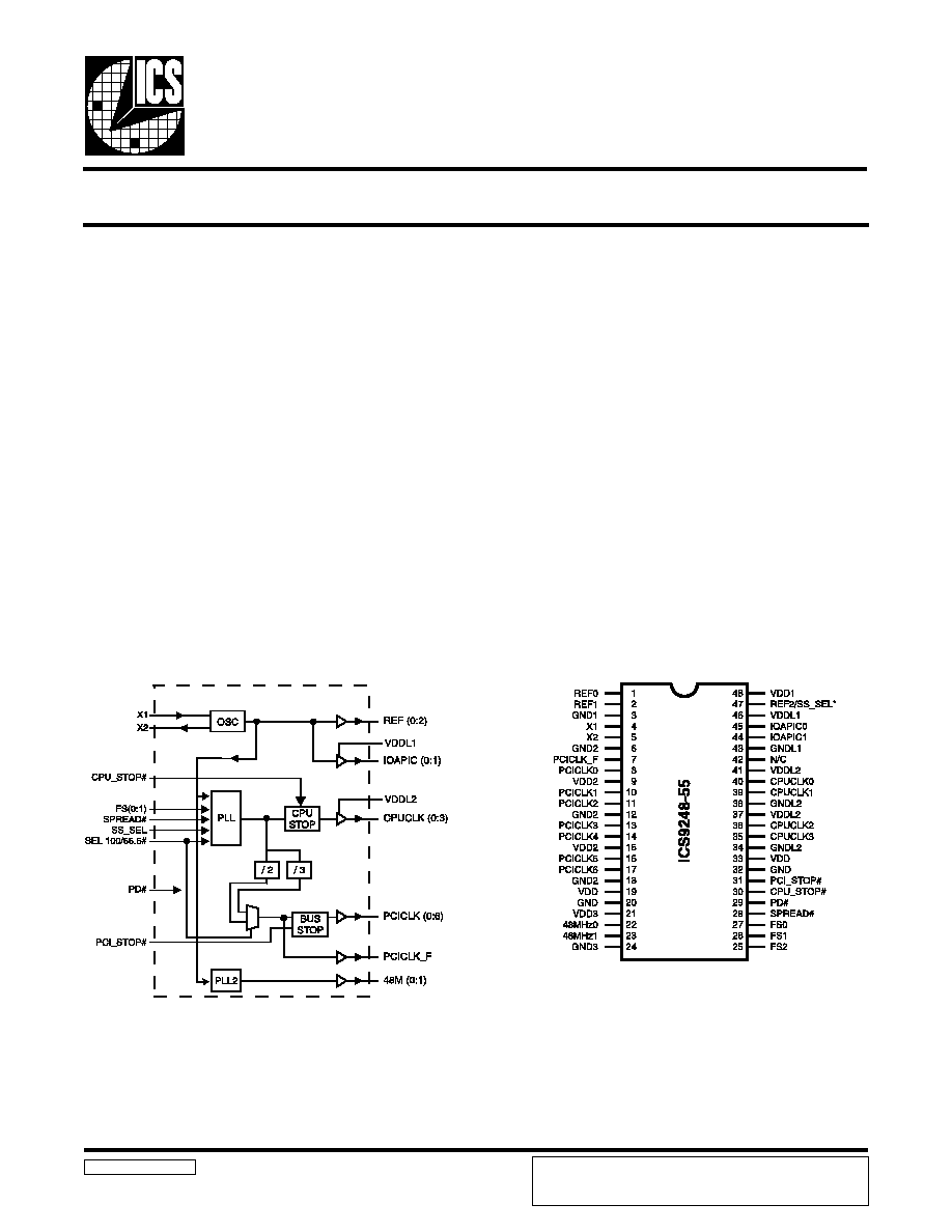
Block Diagram
Pentium/Pro/
II
TM
System Clock Chip
9248-55 Rev B 12/04/98
Pin Configuration
48-Pin SSOP
Pentium is a trademark on Intel Corporation.
Generates system clocks for CPU, IOAPIC, PCI, plus
14.314 MHz REF (0:2), USB, and Super I/O
Supports single or dual processor systems
Supports Spread Spectrum modulation for CPU & PCI
clocks, down spread -0.5%
Skew from CPU (earlier) to PCI clock (rising edges for
100/33.3MHz) 1.5 to 4ns
Two fixed outputs at 48MHz.
Separate 2.5V and 3.3V supply pins
2.5V or 3.3V output: CPU, IOAPIC
3.3V outputs: PCI, REF, 48MHz
No power supply sequence requirements
Uses external 14.318MHz crystal, no external load cap
required for C
L
=18pF crystal
48 pin 300 mil SSOP
The ICS9248-55 is a Clock Synthesizer chip for Pentium and
PentiumPro CPU based Desktop/Notebook systems that will
provide all necessary clock timing.
Features include four CPU and eight PCI clocks. Three
reference outputs are available equal to the crystal frequency.
Additionally, the device meets the Pentium power-up
stabilization requirement, assuring that CPU and PCI clocks
are stable within 2ms after power-up.
PD# pin enables low power mode by stopping crystal OSC
and PLL stages. Other power management features include
CPU_STOP#, which stops CPU (0:3) clocks, and PCI_STOP#,
which stops PCICLK (0:6) clocks.
High drive CPUCLK outputs typically provide greater than 1
V/ns slew rate into 20pF loads. PCICLK outputs typically
provide better than 1V/ns slew rate into 30pF loads while
maintaining 50±5% duty cycle. The REF clock outputs typically
provide better than 0.5V/ns slew rates.
The ICS9248-55 accepts a 14.318MHz reference crystal or
clock as its input and runs on a 3.3V core supply.
Power Groups
VDD = Supply for PLL core
VDD1 = REF (0:2), X1, X2
VDD2 = PCICLK_F, PCICLK (0:6)
VDD3 = 48MHz0, 48MHz1
VDDL1 = IOAPIC (0:1)
VDDL2 = CPUCLK (0:3)
Ground Groups
GND = Ground for PLL core
GND1 = REF (0:2), X1, X2
GND2 = PCICLK_F, PCICLK (0:6)
GND3 = 48MHz0, 48MHz1
GNDL1 = IOAPIC (0:1)
GNDL2 = CPUCLK (0:3)
ICS reserves the right to make changes in the device data identified in
this publication without further notice. ICS advises its customers to
obtain the latest version of all device data to verify that any
information being relied upon by the customer is current and accurate.
* Internal Pull-down Resistor of
240K to GND. on indicated inputs
2
ICS9248-55
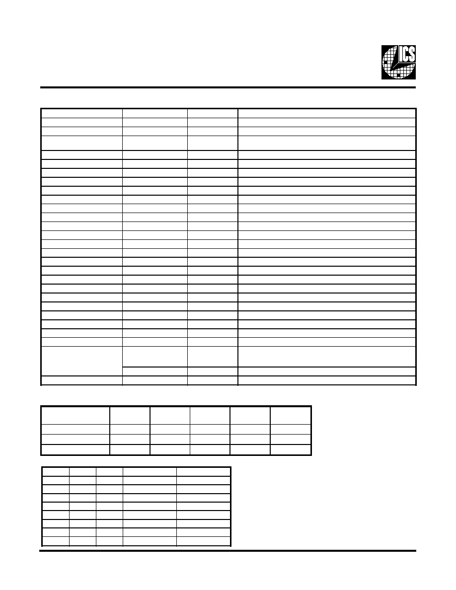
Pin Descriptions
Select Functions
Functionality
CPU
PCI,
PCI_F
REF
IOAPIC
48 MHz
Selection
Tristate
HI - Z
HI - Z
HI - Z
HI - Z
HI - Z
Testmode
TCLK/2
1
TCLK/6
1
TCLK
1
TCLK
1
TCLK/2
1
Spread Spectrum
Modulated
2
Modulated
2
14.318MHz
14.318MHz
48.0MHz
PIN NUMBER
PIN NAME
TYPE
DESCRIPTION
1, 2
REF0, REF1
OUT
14.318MHz clock output
3
GND1
PWR
Ground for REF outputs
4
X1
IN
XTAL_IN 14.318MHz Crystal input, has internal 33pF
load cap and feed back resistor from X2
5
X2
OUT
XTAL_OUT Crystal output, has internal load cap 33pF
6, 12, 18
GND2
PWR
Ground for PCI outputs
7
PCICLK_F
OUT
Free Running PCI output
8, 10, 11, 13, 14, 16, 17
PCICLK (0:6)
OUT
PCI clock outputs. TTL compatible 3.3V
9, 15
VDD2
PWR
Power for PCICLK outputs, nominally 3.3V
19, 33
VDD
PWR
Isolated power for core, nominally 3.3V
20, 32
GND
PWR
Isolated ground for core
21
VDD3
PWR
Power for 48MHz outputs, nominally 3.3V
22, 23
48MHz (0:1)
OUT
48MHz outputs
24
GND3
PWR
Ground for 48MHz outputs
25, 26, 27
FS (0:2)
IN
Frequency Select pins
28
SPREAD#
IN
Enables Spread Spectrum feature when LOW
29
PD#
IN
Powers down chip, active low
30
CPU_STOP#
IN
Halts CPU clocks at logic "0" level when low
31
PCI_STOP#
IN
Halts PCI Bus at logic "0" level when low
37, 41
VDDL2
PWR
Power for CPU outputs, nominally 2.5V
34, 38
GNDL2
PWR
Ground for CPU outputs.
35, 36, 39, 40
CPUCLK (3:0)
OUT
CPU and Host clock outputs @ 2.5V
42
N/C
-
Not internally connected
43
GNDL1
PWR
Ground for IOAPIC outputs
44, 45
IOAPIC (0:1)
OUT
IOAPIC outputs (14.318MHz) @ 2.5V
46
VDDL1
PWR
Power for IOAPIC outputs, nominally 2.5V
47
SS_SEL
IN
±.25% Spread Spectrum Selector at power up.
Logic 0 for Downspread
Logic 1 for Centerspread
REF2
OUT
14.318MHz clock output
48
VDD1
PWR
Supply for REF (0:2), X1, X2, nominal 3.3V
FS2
FS1
FS0
CPU MHz
PCI MHz
0
0
0
133
33.25
0
0
1
83.3
41.65
0
1
0
75
37.5
0
1
1
66.6
33.3
1
0
0
124
41.33
1
0
1
133
44.3
1
1
0
112
37.3
1
1
1
100
33.3
3
ICS9248-55
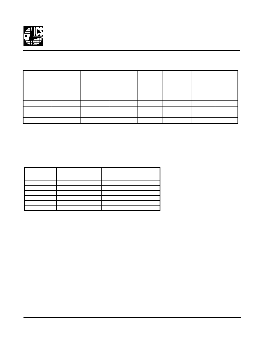
Power Management
ICS9248-55 Power Management Requirements
Clock Enable Configuration
Full clock cycle timing is guaranteed at all times after the system has initially powered up except where noted. During power
up and power down operations using the PD# select pin will not cause clocks of a shorter or longer pulse than that of the
running clock. The first clock pulse coming out of a stopped clock condition may be slightly distorted due to clock network
charging circuitry. Board routing and signal loading may have a large impact on the initial clock distortion also.
Notes.
1. Clock on latency is defined from when the clock enable goes active to when the first valid clock comes out of the device.
2. Clock off latency is defined from when the clock enable goes inactive to when the last clock is driven low out of the device.
3. Power up latency is when PD# goes inactive (high) to when the first valid clocks are output by the device.
4. Power down has controlled clock counts applicable to CPUCLK, PCICLK only.
The REF and IOAPIC will be stopped independent of these.
SIGNAL
SIGNAL STATE
Latency
No. of rising edges of free
running PCICLK
CPU_ STOP#
0 (Disabled)
2
1
1 (Enabled)
1
1
PCI_STOP#
0 (Disabled)
2
1
1 (Enabled)
1
1
PD#
1 (Normal Operation)
3
3ms
0 (Power Down)
4
2max
CPU_STOP#
PCI_STOP#
PWR_DWN#
CPUCLK
PCICLK
Other Clocks,
REF,
IOAPICs,
48 MHz 0
48 MHz 1
Crystal
VCOs
X
X
0
Low
Low
Stopped
Off
Off
0
0
1
Low
Low
Running
Running
Running
0
1
1
Low
Running
Running
Running
Running
1
0
1
Running
Low
Running
Running
Running
1
1
1
Running
Running
Running
Running
Running
4
ICS9248-55
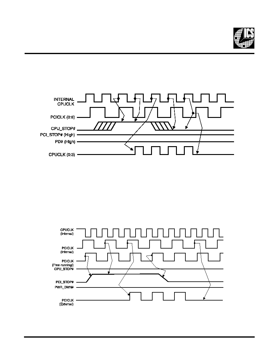
PCI_STOP# Timing Diagram
PCI_STOP# is an asynchronous input to the ICS9248-55. It is used to turn off the PCICLK (0:6) clocks for low power operation.
PCI_STOP# is synchronized by the ICS9248-55 internally. The minimum that the PCICLK (0:6) clocks are enabled (PCI_STOP#
high pulse) is at least 10 PCICLK (0:6) clocks. PCICLK (0:6) clocks are stopped in a low state and started with a full high pulse
width guaranteed. PCICLK (0:6) clock on latency cycles are only one rising PCICLK. Clock off latency is one PCICLK clock.
CPU_STOP# Timing Diagram
CPUSTOP# is an asychronous input to the clock synthesizer. It is used to turn off the CPUCLKs for low power operation.
CPU_STOP# is synchronized by the ICS9248-55. The minimum that the CPUCLK is enabled (CPU_STOP# high pulse) is 100
CPUCLKs. All other clocks will continue to run while the CPUCLKs are disabled. The CPUCLKs will always be stopped in a low
state and start in such a manner that guarantees the high pulse width is a full pulse. CPUCLK on latency is less than 4 CPUCLKs
and CPUCLK off latency is less than 4 CPUCLKs.
Notes:
1. All timing is referenced to the internal CPUCLK.
2. CPU_STOP# is an asynchronous input and metastable conditions may exist. This signal is synchronized to
the CPUCLKs inside the ICS9248-55.
3. All other clocks continue to run undisturbed.
4. PD# and PCI_STOP# are shown in a high (true) state.
Notes:
1. All timing is referenced to the Internal CPUCLK (defined as inside the ICS9248 device.)
2. PCI_STOP# is an asynchronous input, and metastable conditions may exist. This signal is required to be synchronized
inside the ICS9248-55.
3. All other clocks continue to run undisturbed.
4. PD# and CPU_STOP# are shown in a high (true) state.
5
ICS9248-55
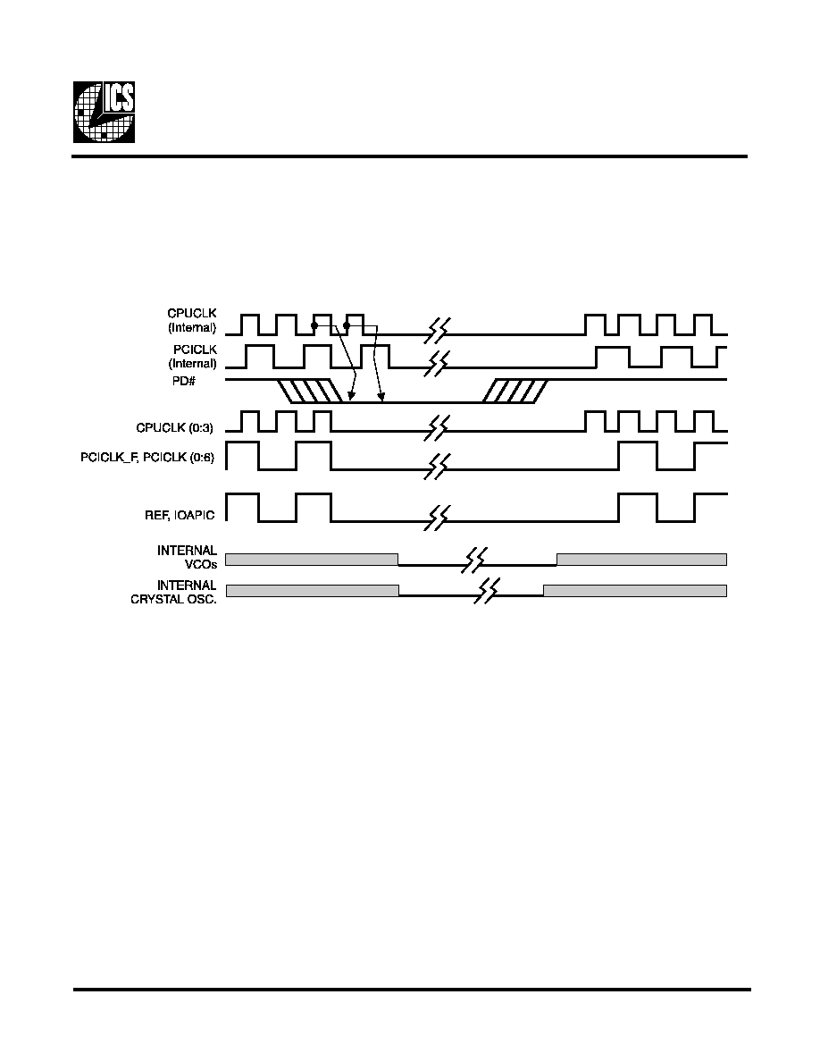
PD# Timing Diagram
The power down selection is used to put the part into a very low power state without turning off the power to the part. PD# is
an asynchronous active low input. This signal is synchronized internally by the ICS9248-55 prior to its control action of
powering down the clock synthesizer. Internal clocks will not be running after the device is put in power down state. When PD#
is active (low) all clocks are driven to a low state and held prior to turning off the VCOs and the Crystal oscillator. The power on
latency is guaranteed to be less than 3ms. The power down latency is less than three CPUCLK cycles. PCI_STOP# and
CPU_STOP# are dont care signals during the power down operations.
Notes:
1. All timing is referenced to the Internal CPUCLK (defined as inside the ICS9248 device).
2. PD# is an asynchronous input and metastable conditions may exist. This signal is synchronized inside the ICS9248.
3. The shaded sections on the VCO and the Crystal signals indicate an active clock is being generated.