Äîêóìåíòàöèÿ è îïèñàíèÿ www.docs.chipfind.ru
Integrated
Circuit
Systems, Inc.
General Description
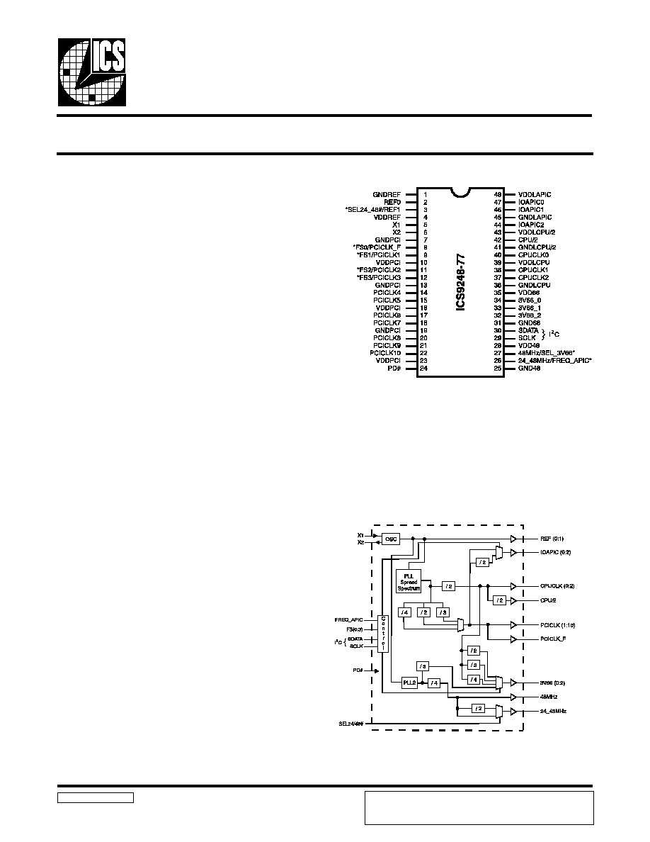
ICS9248-77
Block Diagram
Frequency Timing Generator for PENTIUM II Systems
9248-77 Rev C 10/20/99
Pin Configuration
48-pin SSOP
*120K ohm pull-up to VDD on indicated inputs.
Generates the following system clocks:
- 3 - CPUs @ 2.5V, up to 150MHz.
- 3 - IOAPIC @ 2.5V, PCI or PCI/2
- 3 - 3V66MHz @ 3.3V.
- 11 - PCIs @ 3.3V.
- 1 - 48MHz, @ 3.3V fixed.
- 1 - 24MHz, @ 3.3V fixed.
- 1 - CPU/2, @ 2.5V.
± .25% center spread, or 0 to -.5% down spread.
Uses external 14.318MHz crystal.
The ICS9248-77 is a main clock synthesizer chip for Pentium
II based systems using Rambus Interface DRAMs. This chip
provides all the clocks required for such a system when used
with a Direct Rambus Clock Generator(DRCG) chip such as
the ICS9212-01.
Spread Spectrum may be enabled by driving the SPREAD#
pin active. Spread spectrum typically reduces system EMI by
8dB to 10dB. This simplifies EMI qualification without resorting
to board design iterations or costly shielding. The ICS9248-
77 employs a proprietary closed loop design, which tightly
controls the percentage of spreading over process and
temperature variations.
The CPU/2 clocks are inputs to the DRCG.
ICS reserves the right to make changes in the device data identified in
this publication without further notice. ICS advises its customers to
obtain the latest version of all device data to verify that any
information being relied upon by the customer is current and accurate.
Features
Key Specification
CPU Output Jitter: <250ps
CPU/2 Output Jitter. <250ps
IOAPIC Output Jitter: <500ps
48MHz, 3V66, PCI Output Jitter: <500ps
Ref Output Jitter. <1000ps
CPU Output Skew: <175ps
IOAPIC Output Skew <250ps
PCI Output Skew: <500ps
3V66 Output Skew <250ps
CPU to 3V66 Output Offset: 0.0 - 1.5ns (CPU leads)
3V66 to PCI Output Offset: 1.5 - 4.0ns (3V66 leads)
CPU to IOAPIC Output Offset 1.5 - 4.0ns (CPU leads)
2
ICS9248-77
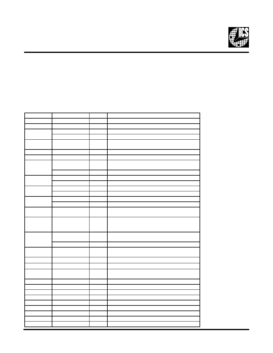
Pin Descriptions
Pin number
Pin name
Type
Description
1, 7, 13, 19, 25, 31 GND
PWR
Ground pins
2
REF0
OUT
14.318MHz reference clock outputs at 3.3V
REF1
OUT
14.318MHz reference clock outputs at 3.3V
SEL24_48
IN
Logic input to select 24 or 48MHz for pin 26 output
4, 10, 16, 23,
28, 35
VDD
PWR
Power pins 3.3V
5
X1
IN
XTAL_IN 14.318MHz crystal input
6
X2
OUT
XTAL_OUT Crystal output
PCICLK_F
OUT
Free running PCI clock at 3.3V. Synchronous to CPU clocks. Not
affected by the PCI_STOP# input.
FS0
IN
Logic - input for frequency selection
PCICLK1
OUT
PCI clock output at 3.3V. Synchronous to CPU clocks.
FS1
IN
Logic - input for frequency selection
PCICLK2
OUT
PCI clock output at 3.3V. Synchronous to CPU clocks.
FS2
IN
Logic - input for frequency selection
PCICLK3
OUT
PCI clock output at 3.3V. Synchronous to CPU clocks.
FS3
IN
Logic - input for frequency selection
14, 15, 17, 18, 20,
21, 22
PCICLK [4:10]
OUT
PCI clock outputs at 3.3V. Synchronous to CPU clocks.
24
PD#
IN
This asynchronous input powers down the chip when drive
active(Low). The internal PLLs are disabled and all the output clocks
are held at a Low state.
24_48MHz
OUT
24 or 48MHz output selectable by
SEL24_48# (0=48MHz 1=24MHz)
FREQ_APIC
IN
Logic input for frequency selection of IOAPIC
27
48MHz/SEL_3V66
OUT/IN
Fixed 48MHz clock output. 3.3V / Logic input to select the
frequency of the 3V66 outputs
29
SCLK
IN
Clock input of I
2
C input
30
SDATA
IN
Data input for I
2
C serial input.
32, 33, 34
3V66[0:2]
OUT
3.3V clock outputs. These outputs are stopped when CPU_STOP#
is driven active..
36
GNDLCPU
PWR
Ground pin for the CPUCLKs
37, 38, 40
CPUCLK[0:2]
OUT
Host bus clock output at 2.5V.
39
VDDLCPU
PWR
Power pin for the CPUCLKs. 2.5V
41
GNDLCPU/2
PWR
Ground pin for the CPU/2 clocks.
42
CPU/2
OUT
2.5V clock outputs at 1/2 CPU frequency.
43
VDDLCPU/2
PWR
Power pin for the CPU/2 clocks. 2.5V
45
GNDLIOAPIC
PWR
Ground pin for the IOAPIC outputs.
44, 46, 47
IOAPIC[0:2]
OUT
IOAPIC clocks at 2.5V. Synchronous with CPUCLKs
48
VDDLIOAPIC
PWR
Power pin for the IOAPIC outputs. 2.5V.
12
26
3
8
9
11
Power Groups:
VDDREF, GNDREF = REF, X1, X2
GNDPCI, VDDPCI = PCICLK
VDD66, GND66 = 3V66
VDD48, GND48 = 48MHz
VDDCOR, GNDCOR = PLL Core
VDDLCPU/2 , GNDLCPU/2 = CPU/2
VDDLIOAPIC, GNDIOAPIC = IOAPIC
3
ICS9248-77
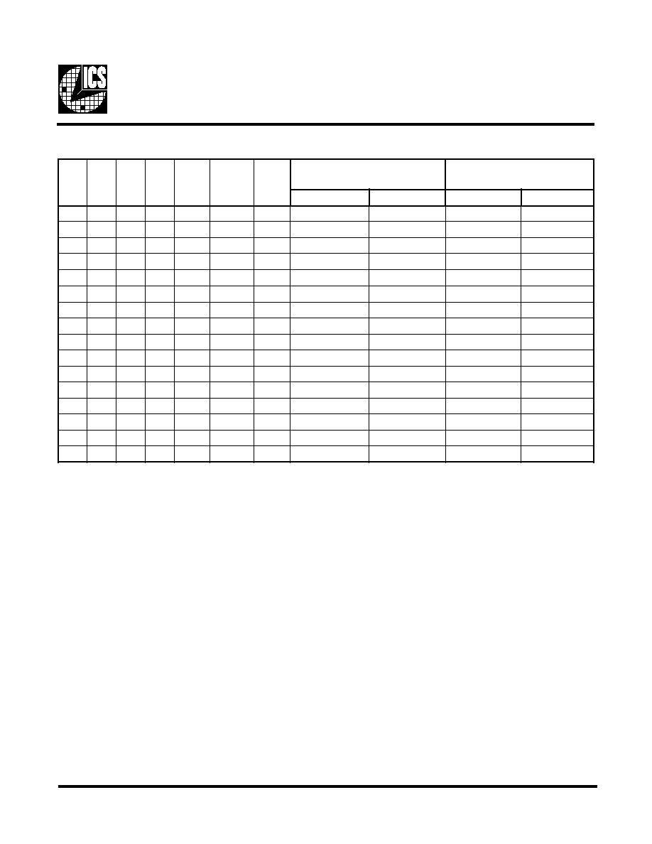
Note:
* These output frequencies are Not synchronous to CPUCLK and Do Not have Spread Spectrum modulation.
Frequency Selection
3
S
F
2
S
F
1
S
F
0
S
F
U
P
C
z
H
M
2
/
U
P
C
z
H
M
I
C
P
z
H
M
z
H
M
6
6
V
3
z
H
M
C
I
P
A
O
I
0
=
6
6
V
3
_
L
E
S
1
=
6
6
V
3
_
L
E
S
0
=
C
I
P
A
_
Q
E
R
F
1
=
I
C
P
A
_
Q
E
R
F
0
0
0
0
5
0
1
5
.
2
5
5
3
0
7
0
7
5
.
7
1
5
3
0
0
0
1
5
7
5
.
7
3
5
.
7
3
*
4
6
5
7
5
7
.
8
1
5
.
7
3
0
0
1
0
3
.
0
0
1
5
1
.
0
5
4
.
3
3
6
.
6
6
6
.
6
6
7
.
6
1
4
.
3
3
0
0
1
1
8
.
6
6
4
.
3
3
4
.
3
3
6
.
6
6
6
.
6
6
7
6
.
6
1
4
.
3
3
0
1
0
0
0
1
1
5
5
6
.
6
3
*
4
6
3
.
3
7
3
.
8
1
6
.
6
3
0
1
0
1
5
1
1
5
.
7
5
3
.
8
3
*
4
6
6
.
6
7
6
1
.
9
1
3
.
8
3
0
1
1
0
7
1
1
5
.
8
5
9
3
*
4
6
8
7
5
.
9
1
9
3
0
1
1
1
0
2
1
0
6
0
4
*
4
6
0
8
0
2
0
4
1
0
0
0
5
2
1
5
.
2
6
6
.
1
4
*
4
6
3
.
3
8
8
.
0
2
6
.
1
4
1
0
0
1
7
2
1
5
.
3
6
3
.
2
4
*
4
6
6
.
4
8
6
1
.
1
2
3
.
2
4
1
0
1
0
3
.
3
3
1
5
.
6
6
3
.
3
3
6
.
6
6
6
.
6
6
6
.
6
1
3
.
3
3
1
0
1
1
5
3
1
5
.
7
6
5
7
.
3
3
5
.
7
6
5
.
7
6
8
.
6
1
5
7
.
3
3
1
1
0
0
7
3
1
5
.
8
6
5
2
.
4
3
5
.
8
6
5
.
8
6
5
2
1
.
7
1
5
2
.
4
3
1
1
0
1
0
4
1
0
7
5
3
0
7
0
7
5
.
7
1
5
3
1
1
1
0
5
4
1
5
.
2
7
5
2
.
6
3
*
4
6
5
.
2
7
5
2
1
.
8
1
5
2
.
6
3
1
1
1
1
0
5
1
5
7
5
.
7
3
*
4
6
5
7
5
7
.
8
1
5
.
7
3
4
ICS9248-77
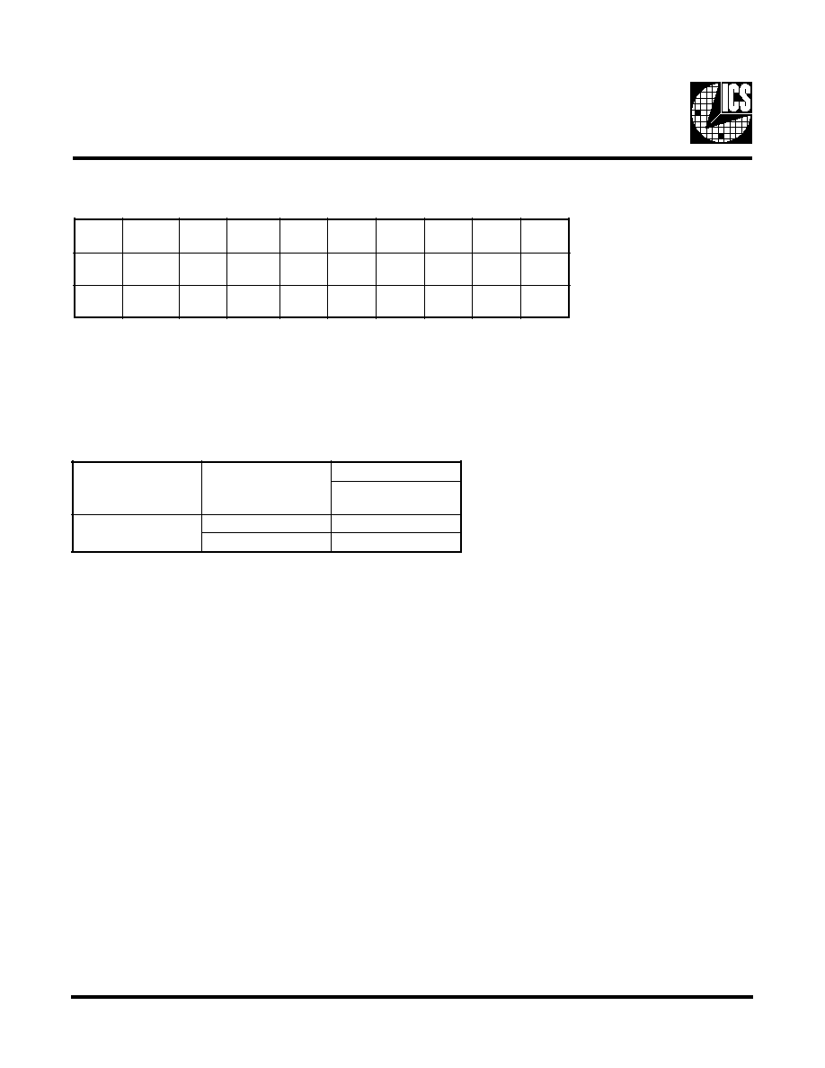
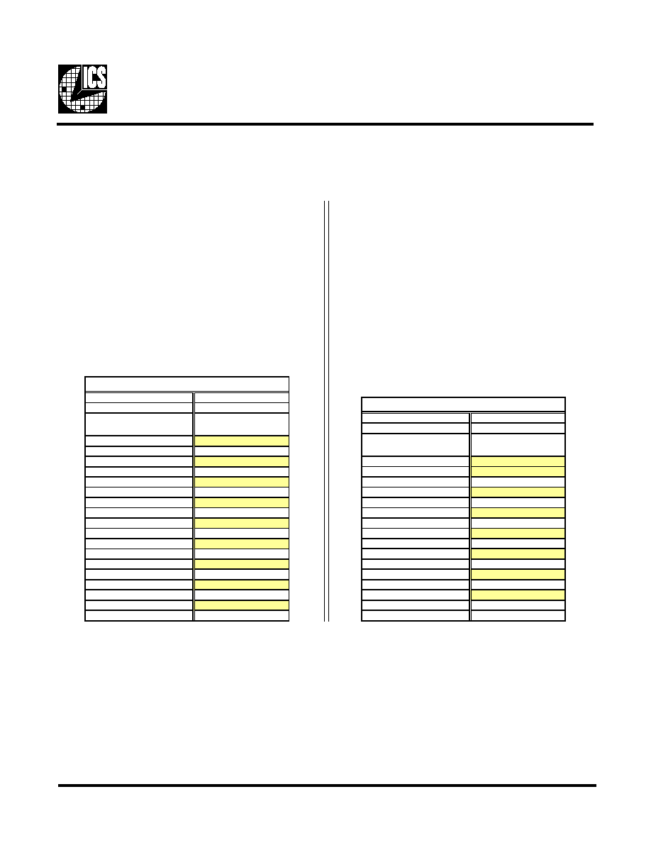
Power Management Features:
Note:
1. LOW means outputs held static LOW as per latency requirement next page.
2. On means active.
3. PD# pulled Low, impacts all outputs including REF and 48 MHz outputs.
#
D
P
K
L
C
U
P
C
2
/
U
P
C
C
I
P
A
O
I
6
6
V
3
I
C
P
F
_
I
C
P
.
F
E
R
z
H
M
8
4
c
s
O
s
O
C
V
0
W
O
L
W
O
L
W
O
L
W
O
L
W
O
L
W
O
L
W
O
L
F
F
O
F
F
O
1
N
O
N
O
N
O
N
O
N
O
N
O
N
O
N
O
N
O
Power Management Requirements:
Note:
1. Clock on/off latency is defined in the number of rising edges of free running PCICLKs between the clock disable goes low/
high to the first valid clock comes out of the device.
2. Power up latency is when PWR_DWN# goes inactive (high to when the first valid clocks are dirven from the device.
l
a
n
g
i
S
e
t
a
t
S
l
a
n
g
i
S
y
c
n
e
t
a
L
f
o
s
e
g
d
e
g
n
i
s
i
r
f
o
.
o
N
K
L
C
I
C
P
#
D
P
)
n
o
i
t
a
r
e
p
o
l
a
m
r
o
n
(
1
S
m
3
)
n
w
o
d
r
e
w
o
p
(
0
.
x
a
m
2
5
ICS9248-77
1.
The ICS clock generator is a slave/receiver, I
2
C component. It can read back the data stored in the latches for verification.
Read-Back will support Intel PIIX4 "Block-Read" protocol.
2.
The data transfer rate supported by this clock generator is 100K bits/sec or less (standard mode)
3.
The input is operating at 3.3V logic levels.
4.
The data byte format is 8 bit bytes.
5.
To simplify the clock generator I
2
C interface, the protocol is set to use only "Block-Writes" from the controller. The
bytes must be accessed in sequential order from lowest to highest byte with the ability to stop after any complete byte
has been transferred. The Command code and Byte count shown above must be sent, but the data is ignored for those
two bytes. The data is loaded until a Stop sequence is issued.
6.
At power-on, all registers are set to a default condition, as shown.
General I
2
C serial interface information
The information in this section assumes familiarity with I
2
C programming.
For more information, contact ICS for an I
2
C programming application note.
How to Write:
Controller (host) sends a start bit.
Controller (host) sends the write address D2
(H)
ICS clock will acknowledge
Controller (host) sends a dummy command code
ICS clock will acknowledge
Controller (host) sends a dummy byte count
ICS clock will acknowledge
Controller (host) starts sending first byte (Byte 0)
through byte 5
ICS clock will acknowledge each byte one at a time.
Controller (host) sends a Stop bit
How to Read:
Controller (host) will send start bit.
Controller (host) sends the read address D3
(H)
ICS clock will acknowledge
ICS clock will send the byte count
Controller (host) acknowledges
ICS clock sends first byte (Byte 0) through byte 5
Controller (host) will need to acknowledge each byte
Controller (host) will send a stop bit
Notes:
Controller (Host)
ICS (Slave/Receiver)
Start Bit
Address
D3
(H)
ACK
Byte Count
ACK
Byte 0
ACK
Byte 1
ACK
Byte 2
ACK
Byte 3
ACK
Byte 4
ACK
Byte 5
ACK
Stop Bit
How to Read:
Controller (Host)
ICS (Slave/Receiver)
Start Bit
Address
D2
(H)
ACK
Dummy Command Code
ACK
Dummy Byte Count
ACK
Byte 0
ACK
Byte 1
ACK
Byte 2
ACK
Byte 3
ACK
Byte 4
ACK
Byte 5
ACK
Stop Bit
How to Write: