Äîêóìåíòàöèÿ è îïèñàíèÿ www.docs.chipfind.ru
Integrated
Circuit
Systems, Inc.
General Description
Features
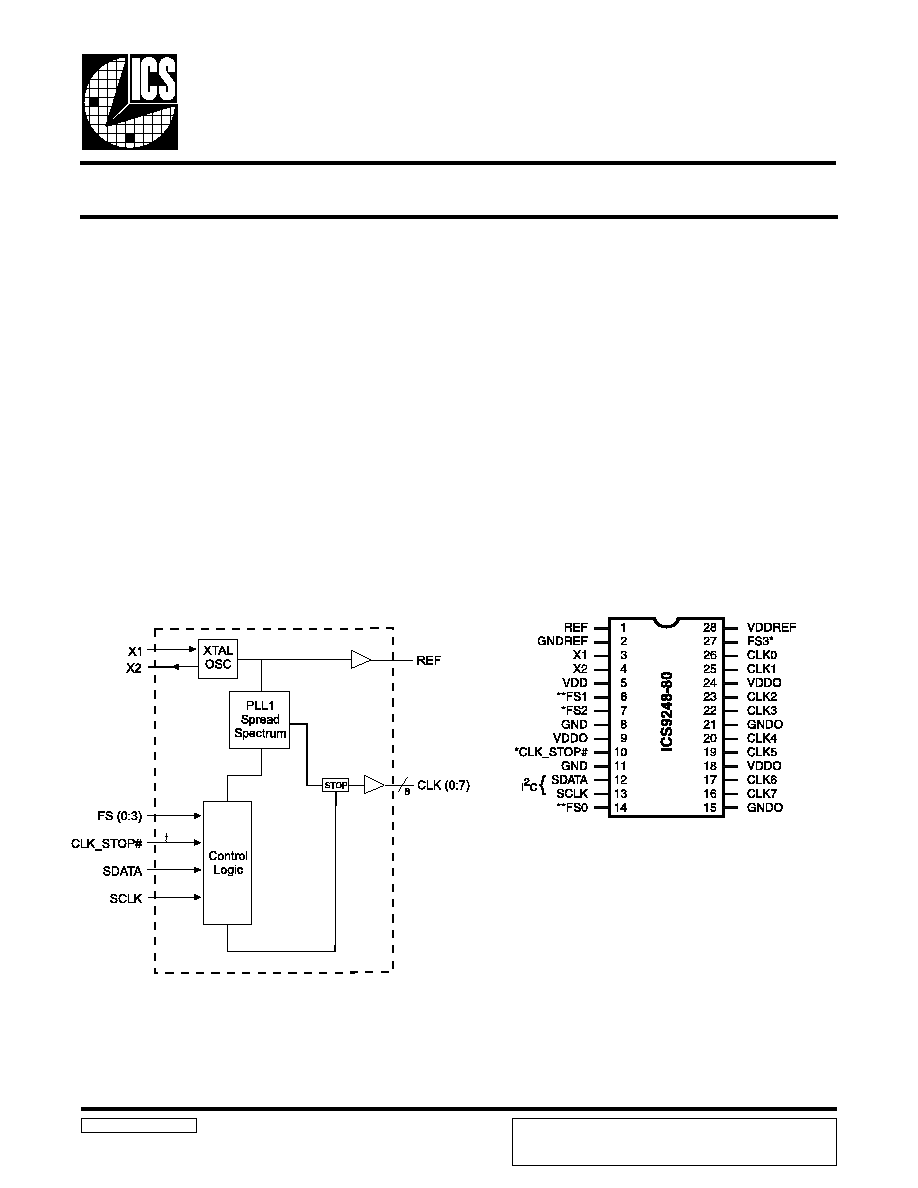
ICS9248-80
Block Diagram
Pentium
II
is a trademark of Intel Corporation
I
2
C is a trademark of Philips Corporation
General Purpose 133MHz System Clock
9248-80 Rev A 3/21/00
Pin Configuration
Extended temperature range (-20°C to +70°C)
Output features:
- 8 CLK outputs @ 3.3V, up to 133.34MHz.
- 1-REF output @ 3.3V, 14.31818MHz.
Spread Spectrum for EMI control
I
2
C interface to stop clocks, select spread and frequency.
Excellent power managment feature through CLK_STOP#
and individual stop clocks through I
2
C.
Input is from a 14.31818MHz crystal.
28-Pin 209 mil SSOP
The ICS9248-80 is a general purpose system clock. It
provides 8 output CLKs, 1 REF CLK and excellent power
management features through CLK_STOP#.
Spread spectrum may be enabled through I
2
C programming.
Spread spectrum typically reduces EMI by 8dB to 10 dB.
This simplifies EMI qualification without resorting to board
design iterations or costly shielding. The ICS9248-80
employs a proprietary closed loop design, which tightly
controls the percentage of spreading over process and
temperature variations.
* These inputs have a 120K internal pull-up to 3.3V.
** These inputs have a 120K internal pull-down to GND.
ICS reserves the right to make changes in the device data identified in
this publication without further notice. ICS advises its customers to
obtain the latest version of all device data to verify that any
information being relied upon by the customer is current and accurate.
2
ICS9248- 80
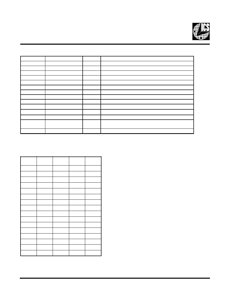
Pin Descriptions
Pin number
Pin name
Type
Description
1
REF
OUT
14.318MHz reference clock outputs at 3.3V
2
GNDREF
PWR
Gnd pin for REF clocks
3
X1
IN
XTAL_IN 14.318MHz crystal input
4
X2
OUT
XTAL_OUT Crystal output
5
VDD
PWR
3.3V power input
6, 7, 14, 27
FS (0:3)
IN
Logic - input for frequency selection
8, 11
GND
PWR
Ground
9, 18, 24
VDDO
PWR
3.3V power for CLK outputs
10
CLK_STOP#
IN
Stops all clock outputs
12
SDATA
IN
Data input for I
2
C serial input.
13
SCLK
IN
Clock input of I
2
C input
15, 21
GNDO
PWR
Ground for CLK outputs
16, 17, 19, 20,
22, 23, 25, 26
CLK (0:7)
OUT
Clock outputs up to 133.34MHz
28
VDDREF
PWR
Power pin for REF clocks
3
S
F
2
S
F
1
S
F
0
S
F
K
L
C
)
z
H
M
(
0
0
0
0
4
3
.
3
3
1
0
0
0
1
1
0
.
5
2
1
0
0
1
0
0
0
.
0
2
1
0
0
1
1
9
9
.
4
1
1
0
1
0
0
9
9
.
9
0
1
0
1
0
1
0
0
.
5
0
1
0
1
1
0
0
0
.
0
0
1
0
1
1
1
0
0
.
5
9
1
0
0
0
0
0
.
0
9
1
0
0
1
1
0
.
5
8
1
0
1
0
0
0
.
5
7
1
0
1
1
0
0
.
0
7
1
1
0
0
7
6
.
6
6
1
1
0
1
0
0
.
0
6
1
1
1
0
9
9
.
4
5
1
1
1
1
3
3
.
3
3
Frequency Selection
3
ICS9248-80
1.
The ICS clock generator is a slave/receiver, I
2
C component. It can read back the data stored in the latches for verification.
Read-Back will support Intel PIIX4 "Block-Read" protocol.
2.
The data transfer rate supported by this clock generator is 100K bits/sec or less (standard mode)
3.
The input is operating at 3.3V logic levels.
4.
The data byte format is 8 bit bytes.
5.
To simplify the clock generator I
2
C interface, the protocol is set to use only "Block-Writes" from the controller. The
bytes must be accessed in sequential order from lowest to highest byte with the ability to stop after any complete byte
has been transferred. The Command code and Byte count shown above must be sent, but the data is ignored for those
two bytes. The data is loaded until a Stop sequence is issued.
6.
At power-on, all registers are set to a default condition, as shown.
General I
2
C serial interface information
The information in this section assumes familiarity with I
2
C programming.
For more information, contact ICS for an I
2
C programming application note.
How to Write:
Controller (host) sends a start bit.
Controller (host) sends the write address D2
(H)
ICS clock will acknowledge
Controller (host) sends a dummy command code
ICS clock will acknowledge
Controller (host) sends a dummy byte count
ICS clock will acknowledge
Controller (host) starts sending first byte (Byte 0)
through byte 5
ICS clock will acknowledge each byte one at a time.
Controller (host) sends a Stop bit
How to Read:
Controller (host) will send start bit.
Controller (host) sends the read address D3
(H)
ICS clock will acknowledge
ICS clock will send the byte count
Controller (host) acknowledges
ICS clock sends first byte (Byte 0) through byte 5
Controller (host) will need to acknowledge each byte
Controller (host) will send a stop bit
Notes:
Controller (Host)
ICS (Slave/Receiver)
Start Bit
Address
D3
(H)
ACK
Byte Count
ACK
Byte 0
ACK
Byte 1
ACK
Byte 2
ACK
Byte 3
ACK
Byte 4
ACK
Byte 5
ACK
Stop Bit
How to Read:
Controller (Host)
ICS (Slave/Receiver)
Start Bit
Address
D2
(H)
ACK
Dummy Command Code
ACK
Dummy Byte Count
ACK
Byte 0
ACK
Byte 1
ACK
Byte 2
ACK
Byte 3
ACK
Byte 4
ACK
Byte 5
ACK
Stop Bit
How to Write:
4
ICS9248- 80
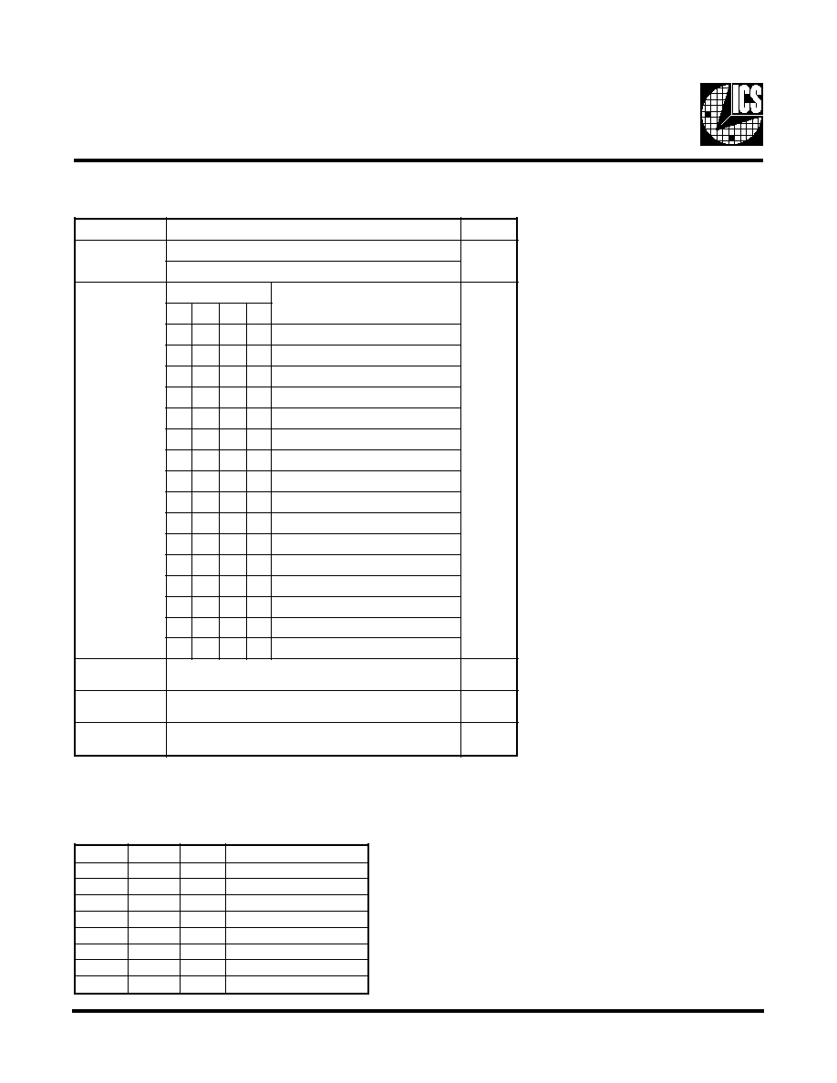
Byte 0: Functionality and frequency select register (Default=0)
(1 = Running, 0 = Stopped Low)
Notes:
1. Default is for frequency control thru hardware pins.
t
i
B
n
o
i
t
p
i
r
c
s
e
D
D
W
P
7
t
i
B
d
a
e
r
p
s
n
w
o
d
%
5
.
0
-
o
t
0
:
0
0
d
a
e
r
p
s
n
w
o
d
%
0
.
1
-
o
t
0
:
1
)
4
:
6
,
2
(
t
i
B
s
t
i
B
y
c
n
e
u
q
e
r
f
K
L
C
1
e
t
o
N
2
6
5
4
0
0
0
0
4
3
.
3
3
1
0
0
0
1
1
0
.
5
2
1
0
0
1
0
0
0
.
0
2
1
0
0
1
1
9
9
.
4
1
1
0
1
0
0
9
9
.
9
0
1
0
1
0
1
0
0
.
5
0
1
0
1
1
0
0
0
.
0
0
1
0
1
1
1
0
0
.
5
9
1
0
0
0
0
0
.
1
9
1
0
0
1
1
0
.
5
8
1
0
1
0
0
0
.
5
7
1
0
1
1
0
0
.
0
7
1
1
0
0
7
6
.
6
6
1
1
0
1
0
0
.
0
6
1
1
1
0
9
9
.
4
5
1
1
1
1
3
3
.
3
3
3
t
i
B
)
3
:
0
(
S
F
e
r
a
w
d
r
a
h
y
b
d
e
t
c
e
l
e
s
s
i
y
c
n
e
u
q
e
r
F
:
0
I
f
o
4
:
6
,
2
s
t
i
b
y
b
d
e
t
c
e
l
e
s
s
i
y
c
n
e
u
q
e
r
f
:
1
2
C
0
1
t
i
B
l
a
m
r
o
N
:
0
d
a
e
r
p
S
:
1
0
0
t
i
B
g
n
i
n
n
u
r
s
t
u
p
t
u
O
:
0
d
e
t
a
t
s
-
i
r
t
s
t
u
p
t
u
O
:
1
0
Byte 1: CLK output control register
(1 = Running, 0 = Stopped Low)
t
i
B
#
n
i
P
D
W
P
n
o
i
t
p
i
r
c
s
e
D
7
t
i
B
6
1
1
7
K
L
C
6
t
i
B
7
1
1
6
K
L
C
5
t
i
B
9
1
1
5
K
L
C
4
t
i
B
0
2
1
4
K
L
C
3
t
i
B
2
2
1
3
K
L
C
2
t
i
B
3
2
1
2
K
L
C
1
t
i
B
5
2
1
1
K
L
C
0
t
i
B
6
2
1
0
K
L
C
5
ICS9248-80
Absolute Maximum Ratings
Core Supply Voltage . . . . . . . . . . . . . . . . . . . . . . 4.6 V
I/O Supply Voltage . . . . . . . . . . . . . . . . . . . . . . . 3.6V
Logic Inputs . . . . . . . . . . . . . . . . . . . . . . . . . . . . GND 0.5 V to V
DD
+0.5 V
Ambient Operating Temperature . . . . . . . . . . . . 20°C to +70°C
Storage Temperature . . . . . . . . . . . . . . . . . . . . . . 65°C to +150°C
Stresses above those listed under Absolute Maximum Ratings may cause permanent damage to the device. These ratings are
stress specifications only and functional operation of the device at these or any other conditions above those listed in the
operational sections of the specifications is not implied. Exposure to absolute maximum rating conditions for extended
periods may affect product reliability.
Electrical Characteristics - Input/Supply/Common Output Parameters
T
A
= -20°C - +70º C; Supply Voltage V
DD
= 3.3 V +/-5% (unless otherwise stated)
PARAMETER
SYMBOL
CONDITIONS
MIN
TYP
MAX
UNITS
Input High Voltage
V
IH
2
V
DD
+0.3
V
Input Low Voltage
V
IL
V
SS
-0.3
0.8
V
Input High Current
I
IH
V
IN
= V
DD
0.1
5
µA
Input Low Current
I
IL1
V
IN
= 0 V; Inputs with no pull-up resistors
-5
2.0
µA
Input Low Current
I
IL2
V
IN
= 0 V; Inputs with pull-up resistors
-200
-100
µA
Operating Supply Current
I
DD2.5OP
C
L
= 0 pF; Select @ 66 MHz
50
100
mA
Input frequency
F
i
V
DD
= 3.3 V;
14.318
MHz
C
IN
Logic Inputs
5
pF
C
INX
X1 & X2 pins
6
pF
Transition Time
1
T
Trans
To first crossing of target Freq.
1.3
2
ms
Settling Time
1
T
S
From first crossing to 1% of target Freq.
0.3
ms
Clk Stabilization
1
T
STAB
From V
DD
= 3.3 V to 1% target Freq.
< 3
3
ms
1
Guaranteed by design, not 100% tested in production.
Input Capacitance
1