Äîêóìåíòàöèÿ è îïèñàíèÿ www.docs.chipfind.ru
Integrated
Circuit
Systems, Inc.
General Description
Features
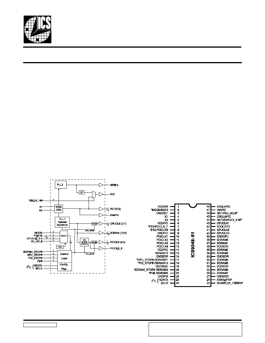
ICS9248- 81
Block Diagram
Pentium is a trademark of Intel Corporation
I
2
C is a trademark of Philips Corporation
Frequency Generator & Integrated Buffers
9248-81 Rev E 10/12/99
Pin Configuration
Generates the following system clocks:
- 3 CPU(2.5V/3.3V) up to 133.3MHz.
- 6 PCI(3.3V) (including 1 free-running)
- 13 SDRAMs(3.3V) up to 133.3MHz.
- 3 REF (3.3V) @ 14.318MHz
- 1 clock @ 24/14.3 MHz selectable output for SIO
- 1 Fixed clock at 48MHz (3.3V)
- 1 IOAPIC @ 2.5V / 3.3V
Skew characteristics:
- CPU CPU<175ps
- SDRAM SDRAM < 250ps
- CPUSDRAM < 500ps
- CPU(early) PCI : 1-4ns (typ. 3ns)
- PCI PCI <500ps
Supports Spread Spectrum modulation ±0.25 & ±0.5%
center spread
Serial I
2
C interface for Power Management, Frequency
Select, Spread Spectrum.
Efficient Power management scheme through PCI,
SDRAM, CPU STOP CLOCKS and PD#.
Uses external 14.318MHz crystal
48 pin 300mil SSOP.
48-Pin SSOP
Power Groups
VDDREF = REF [2:0], X1, X2
VDDPCI = PCICLK_F, PCICLK [4:0]
VDDSD/C = SDRAM [11:0], supply for PLL core, 24 MHz, 48MHz
VDD/CPU = CPUCLK [3:1]
VDDLAPIC = IOAPIC
GNDFIX = Ground for fixed clock PLL and output buffers
* Internal Pull-up Resistor of
120K to 3.3V on indicated inputs
The ICS9248-81 is the single chip clock solution for Desktop/
Notebook designs using the SIS style chipset. It provides all
necessary clock signals for such a system.
Spread spectrum may be enabled through I
2
C programming.
Spread spectrum typically reduces system EMI by 8dB to
10dB. This simplifies EMI qualification without resorting to
board design iterations or costly shielding. The ICS9248-81
employs a proprietary closed loop design, which tightly
controls the percentage of spreading over process and
temperature variations.
Serial programming I
2
C interface allows changing functions,
stop clock programming and frequency selection. The SD_SEL
latched input allows the SDRAM frequency to follow the
CPUCLK frequency(SD_SEL=1) or other clock frequencies
(SD_SEL=0)
ICS reserves the right to make changes in the device data identified in
this publication without further notice. ICS advises its customers to
obtain the latest version of all device data to verify that any
information being relied upon by the customer is current and accurate.
2
ICS9248 -81
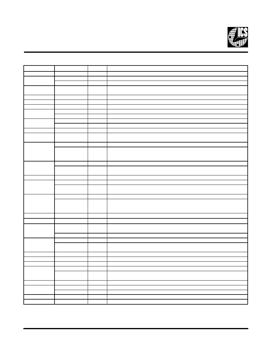
Pin Descriptions
Notes:
1:
Internal Pull-up Resistor of 120K to 3.3V on indicated inputs
2:
Bidirectional input/output pins, input logic levels are latched at internal power-on-reset. Use 10Kohm resistor
to program logic Hi to VDD or GND for logic low.
Pin number
Pin name
Type
D escription
1
VDDR/X
Power
Isolated 3.3 V power for crystal & reference
REF0
Output
3.3V, 14.318 MHz reference clock output.
Mode
Input
Function select pin, 1=desk top mode, 0=mobile mode. Latched input.
3,9,16,22,
27,33,39
GND
Power
3.3 V Ground
4
X1
Input
14.318 MHz crystal input
5
X2
Output
14.318 MHz crystal output
6,14
VDDPCI
Power
3.3 V power for the PCI clock outputs
FS1
Input
Logic input frequency select bit. Input latched at power-on.
PCICLK_F
Output
3.3 V free running PCI clock output, will not be stopped by the PCI_STOP#
PCICLK 0
Output
3.3 V PCI clock outputs, generating timing requirements for Pentium II
FS2
Input
Logic input frequency select bit. Input latched at power-on.
13, 12, 11, 10
PCICLK [4:1]
Output
3.3 V PCI clock outputs, generating timing requirements for Pentium II
15,28,29,31,32,
34,35,37,38
SDRAM 12,
SDRAM [7:0]
Output
SDRAM clock outputs. Frequency is selected by SD-Sel latched input.
SDRAM 11
Output
SDRAM clock outputs. Frequency is selected by SD-Sel latched input.
CPU_STOP#
Input
Asynchronous active low input pin used to stop the CPUCLK in low state,
all other clocks will continue to run. The CPUCLK will have a "Turnon" latency
of at least 3 CPU clocks.
SDRAM 10
Output
SDRAM clock outputs. Frequency is selected by SD-SEL latched input.
PCI-STOP#
Input
Synchronous active low input used to stop the PCICLK in a low state. It will not
effect PCICLK_F or any other outputs.
19
VDDSD/C
Power
3.3 V power for SDRAM outputs and core
SDRAM 9
Output
SDRAM clock outputs. Frequency is selected by SD-Sel latched input.
SDRAM_STOP#
Input
Asynchronous active low input used to stop the SDRAM in a low state.
It will not effect any other outputs.
SDRAM 8
Output
SDRAM clock outputs. Frequency is selected by SD-Sel latched input.
PD#
Input
Asynchronous active low input pin used to power down the device into a low
power state. The internal clocks are disabled and the VCO and the crystal are
stopped. The latency of the power down will not be greater than 3ms.
23
SDATA
Input
Data input for I
2
C serial input.
24
SCLK
Input
Clock input of I
2
C input
SEL24_14#
Input
This input pin controls the frequency of the SIO. If logic 0 at power on
SIO=14.318 MHz . If logic 1 at power-on SIO=24MHz.
SIO
Output
Super I/O output. 24 or 14.318 MHz. Selectable at power-up by SEL24_14MHz
FS0
Input
Logic input frequency select bit. Input latched at power-on.
48 MHz
Output
3.3 V 48 MHz clock output, fixed frequency clock typically used with
USB devices
30,36
VDDSDR
Power
3.3 V power for SDRAM outputs
40,41,43
CPUCLK [3:1]
0utput
2.5 V CPU and Host clock outputs
42
VDDLCPU
Power
2.5 V power for CPU
REF2
Output
3.3V, 14.318 MHz reference clock output.
CPU3.3#_2.5
Input
This pin selects the operating voltage for the CPU. If logic 0 at power on
CPU= 3.3 V and if logic 1 at power on CPU= 2.5 V operating voltage.
45
GNDL
Power
2.5 V Ground for the IOAPIC or CPU
REF1
Output
3.3V, 14.318 MHz reference clock output.
SD_SEL
Input
This input pin controls the frequency of the SDRAM.
47
IOAPIC
Output
2.5V fixed 14.318 MHz IOAPIC clock outputs
48
VDDLAPIC
Power
2.5 V power for IOAPIC
2
1,2
8
1,2
26
1,2
7
1,2
46
1,2
44
1,2
17
1
20
1
18
1
21
1
25
1,2
3
ICS9248-81
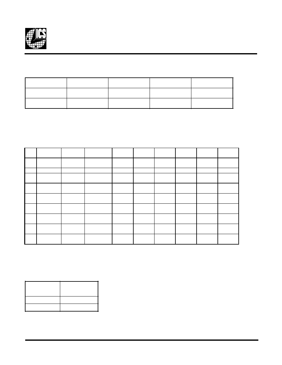
Power Management Functionality
Mode Pin - Power Management Input Control
CPU 3.3#_2.5V Buffer selector for CPUCLK drivers.
PD#
CPU_STOP# PCI_STOP# SDRAM_STOP
PCICLK
(0:4)
SDRAM
(0:12)
PCICLK_F
CPUCLK
Crystal
OSC
VCO
0
X
X
X
Stopped
Low
Stopped
Low
Stopped
Low
Stopped
Low
Stopped
Low
Stopped
Low
1
1
1
1
Running
Running
Running
Running
Running
Running
1
1
1
0
Running
Stopped
Low
Running
Running
Running
Running
1
1
0
1
Stopped
Low
Running
Running
Running
Running
Running
1
1
0
0
Stopped
Low
Stopped
Low
Running
Running
Running
Running
1
0
1
1
Running
Running
Running
Stopped
Low
Running
Running
1
0
1
0
Running
Stopped
Low
Running
Stopped
Low
Running
Running
1
0
0
1
Stopped
Low
Running
Running
Stopped
Low
Running
Running
1
0
0
0
Stopped
Low
Stopped
Low
Running
Stopped
Low
Running
Running
2
n
i
P
,
E
D
O
M
)
t
u
p
n
I
d
e
h
c
t
a
L
(
7
1
n
i
P
8
1
n
i
P
0
2
n
i
P
1
2
n
i
P
0
#
P
O
T
S
_
U
P
C
)
T
U
P
N
I
(
#
P
O
T
S
_
I
C
P
)
T
U
P
N
I
(
#
P
O
T
S
_
M
A
R
D
S
)
T
U
P
N
I
(
#
D
P
)
T
U
P
N
I
(
1
1
1
M
A
R
D
S
)
T
U
P
T
U
O
(
0
1
M
A
R
D
S
)
T
U
P
T
U
O
(
9
M
A
R
D
S
)
T
U
P
T
U
O
(
8
M
A
R
D
S
)
T
U
P
T
U
O
(
5
.
2
_
#
3
.
3
U
P
C
l
e
v
e
l
t
u
p
n
I
)
a
t
a
D
d
e
h
c
t
a
L
(
d
e
t
c
e
l
e
S
r
e
f
f
u
B
:
t
a
n
o
i
t
a
r
e
p
o
r
o
f
1
D
D
V
V
5
.
2
0
D
D
V
V
3
.
3
4
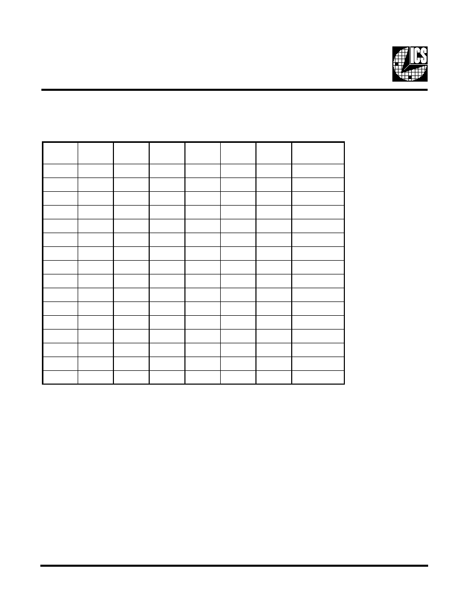
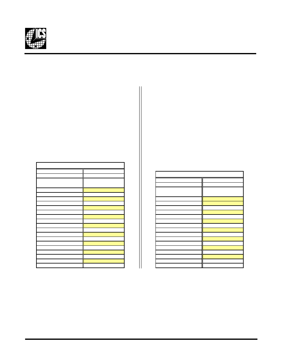
ICS9248 -81
Functionality
V
DD
1, 2, 3, 4 = 3.3V±5%, V
DDL
= 2.5V ±5% or 3.3 ±5%, TA= 0 to 70°C
Crystal (X1, X2) = 14.31818MHz
SD_SEL
FS2
FS1
FS0
CPU
MHZ
SDRAM
MHZ
PCI
MHZ
REF, IOAPIC
MHZ
0
0
0
0
90.00
90.00
30.00
14.318
0
0
0
1
66.70
100.05
33.35
14.318
0
0
1
0
95.00
63.33
31.66
14.318
0
0
1
1
100.00
66.66
33.33
14.318
0
1
0
0
100.00
75.00
30.00
14.318
0
1
0
1
112.00
74.66
37.33
14.318
0
1
1
0
124.00
82.66
31.00
14.318
0
1
1
1
133.30
88.86
33.32
14.318
1
0
0
0
66.70
66.70
33.35
14.318
1
0
0
1
75.00
75.00
30.00
14.318
1
0
1
0
83.30
83.30
33.32
14.318
1
0
1
1
95.00
95.00
31.66
14.318
1
1
0
0
100.00
100.00
33.33
14.318
1
1
0
1
112.00
112.00
37.33
14.318
1
1
1
0
124.00
124.00
31.00
14.318
1
1
1
1
133.30
133.30
33.33
14.318
5
ICS9248-81
1.
The ICS clock generator is a slave/receiver, I
2
C component. It can read back the data stored in the latches for verification.
Read-Back will support Intel PIIX4 "Block-Read" protocol.
2.
The data transfer rate supported by this clock generator is 100K bits/sec or less (standard mode)
3.
The input is operating at 3.3V logic levels.
4.
The data byte format is 8 bit bytes.
5.
To simplify the clock generator I
2
C interface, the protocol is set to use only "Block-Writes" from the controller. The
bytes must be accessed in sequential order from lowest to highest byte with the ability to stop after any complete byte
has been transferred. The Command code and Byte count shown above must be sent, but the data is ignored for those
two bytes. The data is loaded until a Stop sequence is issued.
6.
At power-on, all registers are set to a default condition, as shown.
General I
2
C serial interface information
The information in this section assumes familiarity with I
2
C programming.
For more information, contact ICS for an I
2
C programming application note.
How to Write:
Controller (host) sends a start bit.
Controller (host) sends the write address D2
(H)
ICS clock will acknowledge
Controller (host) sends a dummy command code
ICS clock will acknowledge
Controller (host) sends a dummy byte count
ICS clock will acknowledge
Controller (host) starts sending first byte (Byte 0)
through byte 5
ICS clock will acknowledge each byte one at a time.
Controller (host) sends a Stop bit
How to Read:
Controller (host) will send start bit.
Controller (host) sends the read address D3
(H)
ICS clock will acknowledge
ICS clock will send the byte count
Controller (host) acknowledges
ICS clock sends first byte (Byte 0) through byte 5
Controller (host) will need to acknowledge each byte
Controller (host) will send a stop bit
Notes:
Controller (Host)
ICS (Slave/Receiver)
Start Bit
Address
D3
(H)
ACK
Byte Count
ACK
Byte 0
ACK
Byte 1
ACK
Byte 2
ACK
Byte 3
ACK
Byte 4
ACK
Byte 5
ACK
Stop Bit
How to Read:
Controller (Host)
ICS (Slave/Receiver)
Start Bit
Address
D2
(H)
ACK
Dummy Command Code
ACK
Dummy Byte Count
ACK
Byte 0
ACK
Byte 1
ACK
Byte 2
ACK
Byte 3
ACK
Byte 4
ACK
Byte 5
ACK
Stop Bit
How to Write: