
Integrated
Circuit
Systems, Inc.
General Description
Features
ICS9248- 101
Block Diagram
Pentium is a trademark of Intel Corporation
I
2
C is a trademark of Philips Corporation
Frequency Generator & Integrated Buffers for PENTIUM/Pro
TM
& K6
9248-101 Rev C 2/29/00
Pin Configuration
Up to 137MHz frequency support
Spread Spectrum for EMI control
Serial I
2
C interface for Power Management,
Frequency Select, Spread Spectrum.
Provides the following system clocks
- 4-CPUs @ 2.5/3.3V, up to 137MHz.
(including CPUCLK_F)
- 9-SDRAMs @3.3V, up to 137MHz
(including SDRAM_F)
- 8-PCI @3.3V, CPU/2 or CPU/3
(including 1 free running PCICLK_F)
- 1-24/48MHz @3.3V
- 1-48MHz @3.3V fixed
- 2-REF @3.3V, 14.318MHz.
Efficient Power management scheme through PCI
and STOP CLOCKS
Spread Spectrum � .25%, & 0 to -0.5% down spread
48-Pin SSOP and TSSOP
Power Groups
VDDLCPU, GNDLCPU = CPUCLK [2:0], CPUCLK_F
VDDSDR, GNDSDR = SDRAMCLKS [7:0], SDRAM_F
VDDPCI, GNDPCI = PCICLKS [6:0], PCICLK_F
VDD48, GND48 = 48MHz, 24MHz
VDDREF, GNDREF = REF, X1, X2
VDDCOR = PLL CORE
* Internal Pull-up Resistor of 120K to VDD
The ICS9248-101 is the single chip clock solution for
Notebook designs using the 440BX or the VIA Apollo Pro 133
style chipset. It provides all necessary clock signals for such a
system.
Spread spectrum may be enabled through I
2
C programming.
Spread spectrum typically reduces system EMI by 8dB to
10dB. This simplifies EMI qualification without resorting to
board design iterations or costly shielding. The ICS9248-101
employs a proprietary closed loop design, which tightly
controls the percentage of spreading over process and
temperature variations.
VDDREF
REF0
GNDREF
X1
X2
VDDPCI
*CPU2.5_3.3#/PCICLK_F
*FS3/PCICLK0
GNDPCI
*SEL24_48#/PCICLK1
PCICLK2
PCICLK3
PCICLK4
VDDPCI
BUFFER IN
GNDPCI
PCICLK5
PCICLK6
VDDCOR
PCI_STOP#
*PD#
GND48
SDATA
SCLK
REF1/FS2*
VDDLCPU
CPUCLK_F
CPUCLK0
GNDLCPU
CPUCLK1
CPUCLK2
CLK_STOP#
GNDSDR
SDRAM_F
SDRAM0
SDRAM1
VDDSDR
SDRAM2
SDRAM3
GNDSDR
SDRAM4
SDRAM5
VDDSDR
SDRAM6
SDRAM7
VDD48
48MHz/FS0*
24_48MHz/FS1*
ICS9248-101
1
2
3
4
5
6
7
8
9
10
11
12
13
14
15
16
17
18
19
20
21
22
23
24
48
47
46
45
44
43
42
41
40
39
38
37
36
35
34
33
32
31
30
29
28
27
26
25
{
I C
2
ICS reserves the right to make changes in the device data identified in
this publication without further notice. ICS advises its customers to
obtain the latest version of all device data to verify that any
information being relied upon by the customer is current and accurate.
2
ICS9248-101
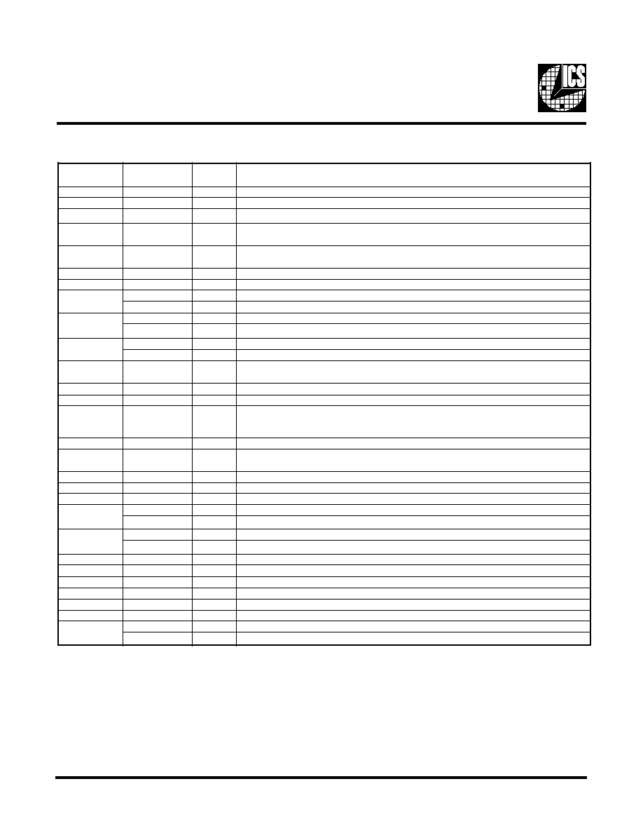
Pin Descriptions
Notes:
1:
Internal Pull-up Resistor of 120K to 3.3V on indicated inputs
2:
Bidirectional input/output pins, input logic levels are latched at internal power-on-reset. Use 10Kohm resistor
to program logic Hi to VDD or GND for logic low.
N
I
P
R
E
B
M
U
N
E
M
A
N
N
I
P
E
P
Y
T
N
O
I
T
P
I
R
C
S
E
D
1
F
E
R
D
D
V
R
W
P
V
3
.
3
l
a
n
i
m
o
n
,
y
l
p
p
u
s
r
e
w
o
p
L
A
T
X
,
f
e
R
2
0
F
E
R
T
U
O
s
d
a
o
l
S
U
B
A
S
I
r
o
f
r
e
f
f
u
b
R
E
G
N
O
R
T
S
e
h
t
s
i
t
u
p
t
u
o
F
E
R
s
i
h
T
.
k
c
o
l
c
e
c
n
e
r
e
f
e
r
z
h
M
8
1
3
.
4
1
0
2
#
P
O
T
S
_
I
C
P
N
I
)
0
=
E
D
O
M
,
e
d
o
m
e
l
i
b
o
m
n
I
(
w
o
l
t
u
p
n
i
n
e
h
w
,
l
e
v
e
l
0
c
i
g
o
l
t
a
s
k
c
o
l
c
]
0
:
6
[
K
L
C
I
C
P
s
t
l
a
H
,
6
1
,
9
,
3
4
4
,
0
4
,
3
3
D
N
G
R
W
P
d
n
u
o
r
G
4
1
X
N
I
k
c
a
b
d
e
e
f
d
n
a
)
F
p
6
3
(
p
a
c
d
a
o
l
l
a
n
r
e
t
n
i
s
a
h
,
t
u
p
n
i
l
a
t
s
y
r
C
2
X
m
o
r
f
r
o
t
s
i
s
e
r
5
2
X
T
U
O
.
z
H
M
8
1
3
.
4
1
y
l
l
a
n
i
m
o
n
,
t
u
p
t
u
o
l
a
t
s
y
r
C
4
1
,
6
I
C
P
D
D
V
R
W
P
V
3
.
3
l
a
n
i
m
o
n
,
]
0
:
6
[
K
L
C
I
C
P
d
n
a
F
_
K
L
C
I
C
P
r
o
f
y
l
p
p
u
S
7
#
3
.
3
_
5
.
2
U
P
C
2
,
1
N
I
.
t
u
p
n
I
d
e
h
c
t
a
L
.
U
P
C
V
3
.
3
=
W
O
L
,
U
P
C
V
5
.
2
=
h
g
i
H
.
V
3
.
3
r
o
5
.
2
s
i
U
P
C
L
D
D
V
r
e
h
t
e
h
w
s
e
t
a
c
i
d
n
I
F
_
K
L
C
I
C
P
T
U
O
.
t
n
e
m
e
g
a
n
a
m
r
e
w
o
p
r
o
f
#
P
O
T
S
_
I
C
P
y
b
d
e
t
c
e
f
f
a
t
o
n
k
c
o
l
c
I
C
P
g
n
i
n
n
u
r
e
e
r
F
8
3
S
F
2
,
1
N
I
.
t
u
p
n
I
d
e
h
c
t
a
L
.
n
i
p
t
c
e
l
e
s
y
c
n
e
u
q
e
r
F
0
K
L
C
I
C
P
T
U
O
)
y
l
r
a
e
U
P
C
(
w
e
k
s
s
n
4
-
1
h
t
i
w
s
k
c
o
l
c
U
P
C
o
t
s
u
o
n
o
r
h
c
n
y
S
.
t
u
p
t
u
o
k
c
o
l
c
I
C
P
0
1
#
8
4
_
4
2
L
E
S
2
,
1
N
I
z
H
M
8
4
=
w
o
L
n
e
h
w
z
H
M
8
4
r
o
4
2
r
e
h
t
i
e
s
t
c
e
l
e
S
1
K
L
C
I
C
P
T
U
O
)
y
l
r
a
e
U
P
C
(
w
e
k
s
s
n
4
-
1
h
t
i
w
s
k
c
o
l
c
U
P
C
o
t
s
u
o
n
o
r
h
c
n
y
S
.
t
u
p
t
u
o
k
c
o
l
c
I
C
P
,
3
1
,
7
1
,
8
1
,
1
1
,
2
1
]
2
:
6
[
K
L
C
I
C
P
T
U
O
)
y
l
r
a
e
U
P
C
(
w
e
k
s
s
n
4
-
1
h
t
i
w
s
k
c
o
l
c
U
P
C
o
t
s
u
o
n
o
r
h
c
n
y
S
.
s
t
u
p
t
u
o
k
c
o
l
c
I
C
P
5
1
N
I
R
E
F
F
U
B
N
I
.
s
t
u
p
t
u
o
M
A
R
D
S
r
o
f
s
r
e
f
f
u
B
t
u
o
n
a
F
o
t
t
u
p
n
I
9
1
R
O
C
D
D
V
R
W
P
V
3
.
3
.
e
r
o
c
L
L
P
e
h
t
r
o
f
n
i
p
r
e
w
o
P
1
2
#
D
P
1
N
I
e
h
T
.
e
t
a
t
s
r
e
w
o
p
w
o
l
a
o
t
n
i
e
c
i
v
e
d
e
h
t
n
w
o
d
r
e
w
o
p
o
t
d
e
s
u
n
i
p
t
u
p
n
i
w
o
l
e
v
i
t
c
a
s
u
o
n
o
r
h
c
n
y
s
A
r
e
w
o
p
e
h
t
f
o
y
c
n
e
t
a
l
e
h
T
.
d
e
p
p
o
t
s
e
r
a
l
a
t
s
y
r
c
e
h
t
d
n
a
O
C
V
e
h
t
d
n
a
d
e
l
b
a
s
i
d
e
r
a
s
k
c
o
l
c
l
a
n
r
e
t
n
i
.
s
m
4
n
a
h
t
r
e
t
a
e
r
g
e
b
t
o
n
l
l
i
w
n
w
o
d
2
2
8
4
D
N
G
R
W
P
.
e
r
o
c
L
L
P
d
e
x
i
f
&
s
r
e
f
f
u
b
t
u
p
t
u
o
z
H
M
8
4
&
4
2
e
h
t
r
o
f
n
i
p
d
n
u
o
r
G
,
2
3
,
1
3
,
9
2
,
8
2
8
3
,
7
3
,
5
3
,
4
3
]
0
:
7
[
M
A
R
D
S
T
U
O
.
)
t
e
s
p
i
h
c
y
b
d
e
l
l
o
r
t
n
o
c
(
n
i
p
N
I
R
E
F
F
U
B
m
o
r
f
s
t
u
p
t
u
o
r
e
f
f
u
B
t
u
o
n
a
F
,
s
t
u
p
t
u
o
k
c
o
l
c
M
A
R
D
S
6
3
,
0
3
R
D
S
D
D
V
R
W
P
.
V
3
.
3
l
a
n
i
m
o
n
,
e
r
o
C
L
L
P
U
P
C
d
n
a
]
0
:
7
[
M
A
R
D
S
r
o
f
y
l
p
p
u
S
3
2
A
T
A
D
S
N
I
I
r
o
f
t
u
p
n
i
a
t
a
D
2
t
u
p
n
i
t
n
a
r
e
l
o
t
V
5
,
t
u
p
n
i
l
a
i
r
e
s
C
4
2
K
L
C
S
N
I
I
f
o
t
u
p
n
i
k
c
o
l
C
2
t
u
p
n
i
t
n
a
r
e
l
o
t
V
5
,
t
u
p
n
i
C
5
2
z
H
M
8
4
_
4
2
T
U
O
0
1
n
i
p
y
b
e
l
b
a
t
c
e
l
e
s
k
c
o
l
c
t
u
p
t
u
o
z
H
M
8
4
r
o
z
H
M
4
2
1
S
F
2
,
1
N
I
.
t
u
p
n
I
d
e
h
c
t
a
L
.
n
i
p
t
c
e
l
e
s
y
c
n
e
u
q
e
r
F
6
2
z
H
M
8
4
T
U
O
k
c
o
l
c
t
u
p
t
u
o
z
H
M
8
4
0
S
F
2
,
1
N
I
t
u
p
n
I
d
e
h
c
t
a
L
.
n
i
p
t
c
e
l
e
s
y
c
n
e
u
q
e
r
F
7
2
8
4
D
D
V
R
W
P
.
e
r
o
c
L
L
P
d
e
x
i
f
d
n
a
s
r
e
f
f
u
b
t
u
p
t
u
o
z
H
M
8
4
&
4
2
r
o
f
r
e
w
o
P
9
3
F
_
M
A
R
D
S
T
U
O
#
P
O
T
S
_
U
P
C
y
b
d
e
t
c
e
f
f
a
t
o
N
.
t
u
p
t
u
o
k
c
o
l
c
M
A
R
D
S
g
n
i
n
n
u
r
e
e
r
F
1
4
#
P
O
T
S
_
K
L
C
N
I
.
w
o
l
n
e
v
i
r
d
n
e
h
w
l
e
v
e
l
"
0
"
c
i
g
o
l
t
a
)
7
:
0
(
M
A
R
D
S
&
,
)
2
:
0
(
K
L
C
U
P
C
s
t
l
a
h
t
u
p
n
i
s
u
o
n
o
r
h
c
n
y
s
a
s
i
h
T
5
4
,
3
4
,
2
4
]
0
:
2
[
K
L
C
U
P
C
T
U
O
U
P
C
L
D
D
V
y
b
d
e
r
e
w
o
p
,
s
t
u
p
t
u
o
k
c
o
l
c
U
P
C
6
4
F
_
K
L
C
U
P
C
T
U
O
#
P
O
T
S
_
U
P
C
e
h
t
y
b
d
e
t
c
e
f
f
a
t
o
N
.
k
c
o
l
c
U
P
C
g
n
i
n
n
u
r
e
e
r
F
7
4
U
P
C
L
D
D
V
R
W
P
V
5
.
2
s
k
c
o
l
c
U
P
C
r
o
f
y
l
p
p
u
S
8
4
1
F
E
R
T
U
O
.
k
c
o
l
c
e
c
n
e
r
e
f
e
r
z
H
M
8
1
3
.
4
1
2
S
F
2
,
1
N
I
t
u
p
n
I
d
e
h
c
t
a
L
.
n
i
p
t
c
e
l
e
s
y
c
n
e
u
q
e
r
F

3
ICS9248-101
1.
The ICS clock generator is a slave/receiver, I
2
C component. It can read back the data stored in the latches for verification.
Read-Back will support Intel PIIX4 "Block-Read" protocol.
2.
The data transfer rate supported by this clock generator is 100K bits/sec or less (standard mode)
3.
The input is operating at 3.3V logic levels.
4.
The data byte format is 8 bit bytes.
5.
To simplify the clock generator I
2
C interface, the protocol is set to use only "Block-Writes" from the controller. The
bytes must be accessed in sequential order from lowest to highest byte with the ability to stop after any complete byte
has been transferred. The Command code and Byte count shown above must be sent, but the data is ignored for those
two bytes. The data is loaded until a Stop sequence is issued.
6.
At power-on, all registers are set to a default condition, as shown.
General I
2
C serial interface information
The information in this section assumes familiarity with I
2
C programming.
For more information, contact ICS for an I
2
C programming application note.
How to Write:
Controller (host) sends a start bit.
Controller (host) sends the write address D2
(H)
ICS clock will acknowledge
Controller (host) sends a dummy command code
ICS clock will acknowledge
Controller (host) sends a dummy byte count
ICS clock will acknowledge
Controller (host) starts sending first byte (Byte 0)
through byte 5
ICS clock will acknowledge each byte one at a time.
Controller (host) sends a Stop bit
How to Read:
Controller (host) will send start bit.
Controller (host) sends the read address D3
(H)
ICS clock will acknowledge
ICS clock will send the byte count
Controller (host) acknowledges
ICS clock sends first byte (Byte 0) through byte 5
Controller (host) will need to acknowledge each byte
Controller (host) will send a stop bit
Notes:
Controller (Host)
ICS (Slave/Receiver)
Start Bit
Address
D3
(H)
ACK
Byte Count
ACK
Byte 0
ACK
Byte 1
ACK
Byte 2
ACK
Byte 3
ACK
Byte 4
ACK
Byte 5
ACK
Stop Bit
How to Read:
Controller (Host)
ICS (Slave/Receiver)
Start Bit
Address
D2
(H)
ACK
Dummy Command Code
ACK
Dummy Byte Count
ACK
Byte 0
ACK
Byte 1
ACK
Byte 2
ACK
Byte 3
ACK
Byte 4
ACK
Byte 5
ACK
Stop Bit
How to Write:

4
ICS9248-101
Functionality
V
DD
= 3.3V�5%, V
DDL
= 2.5V�5% or 3.3�5%, TA=0 to 70�C
Crystal (X1, X2) = 14.31818MHz
3
S
F
2
S
F
1
S
F
0
S
F
U
P
C
)
z
H
M
(
I
C
P
)
z
H
M
(
0
0
0
0
0
0
.
4
2
1
3
3
.
1
4
0
0
0
1
0
0
.
0
2
1
0
0
.
0
4
0
0
1
0
9
9
.
4
1
1
3
3
.
8
3
0
0
1
1
9
9
.
9
0
1
6
6
.
6
3
0
1
0
0
0
0
.
5
0
1
0
0
.
5
3
0
1
0
1
1
3
.
3
8
5
6
.
1
4
0
1
1
0
0
0
.
7
3
1
5
2
.
4
3
0
1
1
1
0
0
.
5
7
0
5
.
7
3
1
0
0
0
0
0
.
0
0
1
3
3
.
3
3
1
0
0
1
0
0
.
5
9
7
6
.
1
3
1
0
1
0
1
3
.
3
8
7
7
.
7
2
1
0
1
1
3
3
.
3
3
1
3
3
.
3
3
1
1
0
0
0
0
.
0
9
0
0
.
0
3
1
1
0
1
2
2
.
6
9
7
0
.
2
3
1
1
1
0
2
8
.
6
6
1
4
.
3
3
1
1
1
1
5
.
1
9
5
.
0
3
Byte0: Functionality and Frequency Select Register (default = 0)
Serial Configuration Command Bitmap
t
i
B
n
o
i
t
p
i
r
c
s
e
D
D
W
P
7
t
i
B
d
a
e
r
p
S
r
e
t
n
e
C
,
n
o
i
t
a
l
u
d
o
M
m
u
r
t
c
e
p
S
d
a
e
r
p
S
%
5
2
.
0
�
-
0
d
a
e
r
p
S
n
w
o
D
%
5
.
0
-
o
t
0
-
1
1
t
i
B
]
4
:
6
,
2
[
]
4
:
6
,
2
[
t
i
B
K
L
C
U
P
C
)
z
H
M
(
K
L
C
I
C
P
)
z
H
M
(
1
e
t
o
N
0
0
0
0
0
0
.
4
2
1
3
3
.
1
4
1
0
0
0
0
0
.
0
2
1
0
0
.
0
4
0
1
0
0
9
9
.
4
1
1
3
3
.
8
3
1
1
0
0
9
9
.
9
0
1
6
6
.
6
3
0
0
1
0
0
0
.
5
0
1
0
0
.
5
3
1
0
1
0
1
3
.
3
8
5
6
.
1
4
0
1
1
0
0
0
.
7
3
1
5
2
.
4
3
1
1
1
0
0
0
.
5
7
0
5
.
7
3
0
0
0
1
0
0
.
0
0
1
3
3
.
3
3
1
0
0
1
0
0
.
5
9
7
6
.
1
3
0
1
0
1
1
3
.
3
8
7
7
.
7
2
1
1
0
1
3
3
.
3
3
1
3
3
.
3
3
0
0
1
1
0
0
.
0
9
0
0
.
0
3
1
0
1
1
2
2
.
6
9
7
0
.
2
3
0
1
1
1
2
8
.
6
6
1
4
.
3
3
1
1
1
1
5
.
1
9
5
.
0
3
3
t
i
B
s
t
u
p
n
i
d
e
h
c
t
a
l
,
t
c
e
l
e
s
e
r
a
w
d
r
a
h
y
b
d
e
t
c
e
l
e
s
s
i
y
c
n
e
u
q
e
r
F
-
0
]
4
:
6
,
2
[
t
i
B
y
b
d
e
t
c
e
l
e
s
s
i
y
c
n
e
u
q
e
r
F
-
1
0
1
t
i
B
l
a
m
r
o
N
-
0
d
e
l
b
a
n
E
m
u
r
t
c
e
p
S
d
a
e
r
p
S
-
1
1
0
t
i
B
g
n
i
n
n
u
R
-
0
s
t
u
p
t
u
o
l
l
a
e
t
a
t
s
i
r
T
-
1
0
Notes:
1, Default at Power-up will be for latched
logic inputs to define frequency. Bit [2,
6:4] are default to 0010.
2, PWD = Power-Up Default
3, When disabling spread spectrum bit7
needs to be set to 0 to maintain nominal
frequency.

5
ICS9248-101
Notes:
1. Inactive means outputs are held LOW and are disabled from switching.
2. Latched Frequency Selects (FS#) will be inverted logic load of the input frequency select pin conditions.
Byte 2: PCI Active/Inactive Register (1 = enable, 0 = disable)
t
i
B
#
n
i
P
D
W
P
n
o
i
t
p
i
r
c
s
e
D
7
t
i
B
7
1
)
t
c
a
n
I
/
t
c
A
(
F
_
K
L
C
I
C
P
6
t
i
B
8
1
1
)
t
c
a
n
I
/
t
c
A
(
6
K
L
C
I
C
P
5
t
i
B
7
1
1
)
t
c
a
n
I
/
t
c
A
(
5
K
L
C
I
C
P
4
t
i
B
3
1
1
)
t
c
a
n
I
/
t
c
A
(
4
K
L
C
I
C
P
3
t
i
B
2
1
1
)
t
c
a
n
I
/
t
c
A
(
3
K
L
C
I
C
P
2
t
i
B
1
1
1
)
t
c
a
n
I
/
t
c
A
(
2
K
L
C
I
C
P
1
t
i
B
0
1
1
)
t
c
a
n
I
/
t
c
A
(
1
K
L
C
I
C
P
0
t
i
B
8
1
)
t
c
a
n
I
/
t
c
A
(
0
K
L
C
I
C
P
Byte 1: CPU, Active/Inactive Register (1 = enable, 0 = disable)
t
i
B
#
n
i
P
D
W
P
n
o
i
t
p
i
r
c
s
e
D
7
t
i
B
-
1
)
d
e
v
r
e
s
e
R
(
6
t
i
B
6
4
1
)
t
c
a
n
I
/
t
c
A
(
F
_
K
L
C
U
P
C
5
t
i
B
-
1
)
d
e
v
r
e
s
e
R
(
4
t
i
B
-
1
)
d
e
v
r
e
s
e
R
(
3
t
i
B
9
3
1
)
t
c
a
n
I
/
t
c
A
(
F
_
M
A
R
D
S
2
t
i
B
2
4
1
)
t
c
a
n
I
/
t
c
A
(
2
K
L
C
U
P
C
1
t
i
B
3
4
1
)
t
c
a
n
I
/
t
c
A
(
1
K
L
C
U
P
C
0
t
i
B
5
4
1
)
t
c
a
n
I
/
t
c
A
(
0
K
L
C
U
P
C
Byte 3: SDRAM Active/Inactive Register (1 = enable, 0 = disable)
t
i
B
#
n
i
P
D
W
P
n
o
i
t
p
i
r
c
s
e
D
7
t
i
B
-
1
)
d
e
v
r
e
s
e
R
(
6
t
i
B
-
1
)
d
e
v
r
e
s
e
R
(
5
t
i
B
-
1
)
d
e
v
r
e
s
e
R
(
4
t
i
B
-
1
)
d
e
v
r
e
s
e
R
(
3
t
i
B
8
2
1
)
e
v
i
t
c
a
n
I
/
e
v
i
t
c
A
(
7
M
A
R
D
S
2
t
i
B
9
2
1
)
e
v
i
t
c
a
n
I
/
e
v
i
t
c
A
(
6
M
A
R
D
S
1
t
i
B
1
3
1
)
e
v
i
t
c
a
n
I
/
e
v
i
t
c
A
(
5
M
A
R
D
S
0
t
i
B
2
3
1
)
e
v
i
t
c
a
n
I
/
e
v
i
t
c
A
(
4
M
A
R
D
S

6
ICS9248-101
Byte 4: Reserved Active/Inactive Register (1 = enable, 0 = disable)
Byte 5: Peripheral Active/Inactive Register (1 = enable, 0 = disable)
Notes:
1. Inactive means outputs are held LOW and are disabled from switching.
2. Latched Frequency Selects (FS#) will be inverted logic load of the input frequency select pin conditions.
t
i
B
#
n
i
P
D
W
P
n
o
i
t
p
i
r
c
s
e
D
7
t
i
B
-
1
)
d
e
v
r
e
s
e
R
(
6
t
i
B
-
1
)
d
e
v
r
e
s
e
R
(
5
t
i
B
-
1
#
)
8
4
_
4
2
L
E
S
(
4
t
i
B
-
1
)
d
e
v
r
e
s
e
R
(
3
t
i
B
-
X
#
1
S
F
d
e
h
c
t
a
L
2
t
i
B
-
1
)
d
e
v
r
e
s
e
R
(
1
t
i
B
-
X
#
3
S
F
d
e
h
c
t
a
L
0
t
i
B
-
1
)
d
e
v
r
e
s
e
R
(
t
i
B
#
n
i
P
D
W
P
n
o
i
t
p
i
r
c
s
e
D
7
t
i
B
4
3
1
)
t
c
a
n
I
/
t
c
A
(
3
M
A
R
D
S
6
t
i
B
5
3
1
)
t
c
a
n
I
/
t
c
A
(
2
M
A
R
D
S
5
t
i
B
7
3
1
)
t
c
a
n
I
/
t
c
A
(
1
M
A
R
D
S
4
t
i
B
8
3
1
)
t
c
a
n
I
/
t
c
A
(
0
M
A
R
D
S
3
t
i
B
6
2
1
)
t
c
a
n
I
/
t
c
A
(
z
H
M
8
4
2
t
i
B
5
2
1
)
t
c
a
n
I
/
t
c
A
(
z
H
M
4
2
1
t
i
B
8
4
1
)
t
c
a
n
I
/
t
c
A
(
1
F
E
R
0
t
i
B
2
1
)
t
c
a
n
I
/
t
c
A
(
0
F
E
R

7
ICS9248-101
CLK_STOP# Timing Diagram
CLK_STOP# is an asychronous input to the clock synthesizer. It is used to turn off the CPU clocks for low power operation.
CLK_STOP# is synchronized by the ICS9248-101. The minimum that the CPU clock is enabled (CLK_STOP# high pulse) is 100
CPU clocks. All other clocks will continue to run while the CPU clocks are disabled. The CPU clocks will always be stopped in
a low state and start in such a manner that guarantees the high pulse width is a full pulse. CPU clock on latency is less than 4
CPU clocks and CPU clock off latency is less than 4 CPU clocks.
Notes:
1. All timing is referenced to the internal CPU clock.
2. CLK_STOP# is an asynchronous input and metastable conditions may exist. This signal is synchronized
to the CPU clocks inside the ICS9248-101.
3. SDRAM-F output is controlled by Buffer in signal, not affected by the ICS9248-101
CLK_STOP# signal. SDRAM [7:0] are controlled as shown.
4. All other clocks continue to run undisturbed.
PCICLK [6:0]
SDRAM [7:0]
CPUCLK [2:0]
CPUCLK _F
SDRAM_F
PCI_STOP# (High)
CLK_STOP#
INTERNAL
CPUCLK

8
ICS9248-101
PD# Timing Diagram
The power down selection is used to put the part into a very low power state without turning off the power to the part. PD# is
an asynchronous active low input. This signal needs to be synchronized internal to the device prior to powering down the clock
synthesizer.
Internal clocks are not running after the device is put in power down. When PD# is active low all clocks need to be driven to a
low value and held prior to turning off the VCOs and crystal. The power up latency needs to be less than 4 mS. The power down
latency should be as short as possible but conforming to the sequence requirements shown below. PCI_STOP# and CLK_STOP#
are considered to be don't cares during the power down operations. The REF and 48MHz clocks are expected to be stopped in
the LOW state as soon as possible. Due to the state of the internal logic, stopping and holding the REF clock outputs in the
LOW state may require more than one clock cycle to complete.
Notes:
1. All timing is referenced to the Internal CPUCLK (defined as inside the ICS9248 device).
2. As shown, the outputs Stop Low on the next falling edge after PD# goes low.
3. PD# is an asynchronous input and metastable conditions may exist. This signal is synchronized inside this part.
4. The shaded sections on the VCO and the Crystal signals indicate an active clock.
5. Diagrams shown with respect to 133MHz. Similar operation when CPU is 100MHz.
CPUCLK
PCICLK
VCO
Crystal
PD#

9
ICS9248-101
PCI_STOP# Timing Diagram
PCI_STOP# is an asynchronous input to the ICS9248-101. It is used to turn off the PCICLK [6:0] clocks for low power
operation. PCI_STOP# is synchronized by the ICS9248-101 internally. The minimum that the PCICLK [6:0] clocks are enabled
(PCI_STOP# high pulse) is at least 10 PCICLK [6:0] clocks. PCICLK [6:0] clocks are stopped in a low state and started with a full
high pulse width guaranteed. PCICLK [6:0] clock on latency cycles are only three rising PCICLK clocks, off latency is one
PCICLK clock.
Notes:
1. All timing is referenced to the Internal CPUCLK (defined as inside the ICS9248 device.)
2. PCI_STOP# is an asynchronous input, and metastable conditions may exist. This signal is required to be synchronized
inside the ICS9248.
3. All other clocks continue to run undisturbed.
4. CLK_STOP# is shown in a high (true) state.
CPUCLK
(Internal)
PCICLK_F
(Internal)
PCICLK_F
(Free-running)
CLK_STOP#
PCICLK [6:0]
PCI_STOP#

10
ICS9248-101
Shared Pin Operation -
Input/Output Pins
Fig. 1
The I/O pins designated by (input/output) on the ICS9248-
101 serve as dual signal functions to the device. During
initial power-up, they act as input pins. The logic level
(voltage) that is present on these pins at this time is read and
stored into a 4-bit internal data latch. At the end of Power-On
reset, (see AC characteristics for timing values), the device
changes the mode of operations for these pins to an output
function. In this mode the pins produce the specified buffered
clocks to external loads.
To program (load) the internal configuration register for these
pins, a resistor is connected to either the VDD (logic 1)
power supply or the GND (logic 0) voltage potential. A 10
Kilohm(10K) resistor is used to provide both the solid CMOS
programming voltage needed during the power-up
programming period and to provide an insignificant load on
the output clock during the subsequent operating period.
Figs. 1 and 2 show the recommended means of implementing
this function. In Fig. 1 either one of the resistors is loaded
onto the board (selective stuffing) to configure the devices
internal logic. Figs. 2a and b provide a single resistor loading
option where either solder spot tabs or a physical jumper
header may be used.
These figures illustrate the optimal PCB physical layout
options. These configuration resistors are of such a large
ohmic value that they do not effect the low impedance clock
signals. The layouts have been optimized to provide as little
impedance transition to the clock signal as possible, as it
passes through the programming resistor pad(s).

11
ICS9248-101
Fig. 2a
Fig. 2b

12
ICS9248-101
Absolute Maximum Ratings
Supply Voltage. . . . . . . . . . . . . . . . . . . . . . . . . . . 7.0 V
Logic Inputs . . . . . . . . . . . . . . . . . . . . . . . . . . . . . GND 0.5 V to V
DD
+0.5 V
Ambient Operating Temperature . . . . . . . . . . . . 0�C to +70�C
Case Temperature . . . . . . . . . . . . . . . . . . . . . . . . 115�C
Storage Temperature . . . . . . . . . . . . . . . . . . . . . . 65�C to +150�C
Stresses above those listed under Absolute Maximum Ratings may cause permanent damage to the device. These ratings are stress
specifications only and functional operation of the device at these or any other conditions above those listed in the operational
sections of the specifications is not implied. Exposure to absolute maximum rating conditions for extended periods may affect
product reliability.
Ele ctrical Characte ristics - Input/Supply /Com m on Output Param e te rs
T
A
= 0 - 70C; Supply Voltage V
D D
= V
D D L
= 3.3 V +/-5% (unles s otherwis e s tated)
PA RA M ETER
SYM BOL
CONDITIONS
M IN
TYP
M A X
UNITS
Input High Voltage
V
IH
2
V
D D
+0.3
V
Input Low Voltage
V
IL
V
SS
-0.3
0.8
V
C
L
= 0 pF; Select @ 66M Hz
90
150
C
L
= 0 pF; Select @ 100M Hz
120
170
C
L
= 0 pF; Select @ 133M Hz
151
180
Powerdown Current
I
D D P D
CL = 0 pF; Input address VDD or GND
250
600
�A
Input Frequency
F
i
V
D D
= 3.3 V
12
14.318
16
M Hz
Input Capacitance
1
C
IN
Logic Inputs
5
pF
C
IN X
X1 & X2 pins
27
36
45
pF
Clk Stabilization
1
T
STA B
From V
D D
= 3.3 V to 1% target Freq.
5.5
ms
Skew
1
t
CP U -P CI1
V
T
= 1.5 V
1
2.8
4
ns
1
Guaranteed by des ign, not 100% tes ted in production.
mA
Operating Supply
Current
I
DD3.3 OP
Ele ctrical Characte ristics - Input/Supply /Com m on Output Param e te rs
T
A
= 0 - 70� C; Supply Voltage V
D D
= 3.3 V +/-5%, V
D D L
= 2.5 V +/-5% (unles s otherwis e s tated)
PA RA M ETER
SYM BOL
CONDITIONS
M IN
TYP
M A X
UNITS
C
L
= 0 pF; Select @ 66.8 M Hz
8
15
C
L
= 0 pF; Select @ 100 M Hz
11
18
C
L
= 0 pF; Select @ 133 M Hz
17
20
Powerdown Current
I
D D L P D
CL = 0 pF; Input address VDD or GN D
<1
10
�
A
Skew
1
t
CP U -P CI2
V
T
= 1.5 V; V
TL
= 1.25 V
1
2.4
4
ns
1
Guaranteed by des ign, not 100% tes ted in production.
I
D D L 2 .5
Operating SupplyCurrent
mA

13
ICS9248-101
Electrical Characteristics - CPU
T
A
= 0 - 70C; V
DD
= 3.3 V +/-5%; C
L
= 20 pF
PARAMETER
SYMBOL
CONDITIONS
MIN
TYP
MAX
UNITS
Output High Voltage
V
OH2A
I
OH
= -20 mA
2.4
2.85
V
Output Low Voltage
V
OL2A
I
OL
= 12 mA
0.31
0.4
V
Output High Current
I
OH2A
V
OH
= 2.0 V
-45
-27
mA
Output Low Current
I
OL2A
V
OL
= 0.8 V
22
29
mA
Rise Time
1
t
r2A
V
OL
= 0.4 V, V
OH
= 2.4 V
1.5
2
ns
Fall Time
1
t
f2A
V
OH
= 2.4 V, V
OL
= 0.4 V
1.4
2
ns
Duty Cycle
1
d
t2A
V
T
= 1.5 V
45
55
%
Skew window
1
t
sk2A
V
T
= 1.5 V
80
175
ps
Jitter, Cycle-to-cycle
1
t
jcyc-cyc2A
V
T
= 1.5 V
200
250
ps
1
Guaranteed by design, not 100% tested in production.
Electrical Characteristics - CPU
T
A
= 0 - 70C; V
DDL
= 2.5 V +/-5%; C
L
= 20 pF
PARAMETER
SYMBOL
CONDITIONS
MIN
TYP
MAX
UNITS
Output High Voltage
V
OH2B
I
OH
= -12 mA
2
2.3
V
Output Low Voltage
V
OL2B
I
OL
= 12 mA
0.31
0.4
V
Output High Current
I
OH2B
V
OH
= 1.7 V
-39
-21
mA
Output Low Current
I
OL2B
V
OL
= 0.7 V
22
26
mA
Rise Time
1
t
r2B
V
OL
= 0.4 V, V
OH
= 2.0 V
1.3
1.6
ns
Fall Time
1
t
f2B
V
OH
= 2.0 V, V
OL
= 0.4 V
1.4
1.6
ns
V
T
= 1.25 V, < 133 MHz
45
47.5
55
V
T
= 1.25 V, >= 133 MHz
42
47
52
Skew window
1
t
sk2B
V
T
= 1.25 V
70
175
ps
Jitter, Cycle-to-cycle
1
t
jcyc-cyc2B
V
T
= 1.25 V
200
300
ps
1
Guaranteed by design, not 100% tested in production.
%
d
t2B
Duty Cycle
1

14
ICS9248-101
Electrical Characteristics - PCI
T
A
= 0 - 70C; V
DD
= V
DDL
= 3.3 V +/-5%; C
L
= 30 pF
PARAMETER
SYMBOL
CONDITIONS
MIN
TYP
MAX
UNITS
Output High Voltage
V
OH1
I
OH
= -18 mA
2.4
3
V
Output Low Voltage
V
OL1
I
OL
= 9.4 mA
0.2
0.4
V
Output High Current
I
OH1
V
OH
= 2.0 V
-62
-33
mA
Output Low Current
I
OL1
V
OL
= 0.8 V
38
43
mA
Rise Time
1
t
r1
V
OL
= 0.4 V, V
OH
= 2.4 V
1.5
2
ns
Fall Time
1
t
f1
V
OH
= 2.4 V, V
OL
= 0.4 V
1.5
2
ns
Duty Cycle
1
d
t1
V
T
= 1.5 V
45
50
55
%
Skew window
1
t
sk1
V
T
= 1.5 V
180
500
ps
Jitter, One Sigma
1
t
j1s1
V
T
= 1.5 V
15
150
ps
Jitter, Absolute
1
t
jabs1
V
T
= 1.5 V
-250
75
250
ps
1
Guaranteed by design, not 100% tested in production.
Electrical Characteristics - SDRAM
T
A
= 0 - 70C; V
DD
= V
DDL
= 3.3 V +/-5%; C
L
= 30 pF
PARAMETER
SYMBOL
CONDITIONS
MIN
TYP
MAX
UNITS
Output High Voltage
V
OH3
I
OH
= -28 mA
2.4
3
V
Output Low Voltage
V
OL3
I
OL
= 19 mA
0.3
0.4
V
Output High Current
I
OH3
V
OH
= 2.0 V
-69
-46
mA
Output Low Current
I
OL3
V
OL
= 0.8 V
32
42
mA
Rise Time
1
T
r3
V
OL
= 0.4 V, V
OH
= 2.4 V
1
1.3
ns
Fall Time
1
T
f3
V
OH
= 2.4 V, V
OL
= 0.4 V
1.3
2
ns
Duty Cycle
1
D
t3
V
T
= 1.5 V
45
50
55
%
Skew window
1
T
sk3
V
T
= 1.5 V
185
250
ps
Propagation Time
1
(Buffer In to output)
T
sk3
V
T
= 1.5 V
4
5
ns
1
Guaranteed by design, not 100% tested in production.

15
ICS9248-101
Electrical Characteristics - 24,48MHz, REF(0:1)
T
A
= 0 - 70C; V
DD
= V
DDL
= 3.3 V +/-5%; C
L
= 10 - 20 pF (unless otherwise stated)
PARAMETER
SYMBOL
CONDITIONS
MIN
TYP
MAX
UNITS
Output High Voltage
V
OH5
I
OH
= -14 mA
2.4
2.6
V
Output Low Voltage
V
OL5
I
OL
= 6 mA
0.22
0.4
V
Output High Current
I
OH5
V
OH
= 2.0 V
-32
-20
mA
Output Low Current
I
OL5
V
OL
= 0.8 V
16
22
mA
Rise Time
1
t
r5
V
OL
= 0.4 V, V
OH
= 2.4 V
2
4
ns
Fall Time
1
t
f5
V
OH
= 2.4 V, V
OL
= 0.4 V
2
4
ns
Duty Cycle
1
d
t5
V
T
= 1.5 V
45
1
55
%
Jitter, One Sigma
1
t
j1s5
V
T
= 1.5 V
150
250
ps
Jitter, Absolute
1
t
jabs5
V
T
= 1.5 V
-600
600
ps
1
Guaranteed by design, not 100% tested in production.

16
ICS9248-101
ICS reserves the right to make changes in the device data identified in
this publication without further notice. ICS advises its customers to
obtain the latest version of all device data to verify that any
information being relied upon by the customer is current and accurate.
Ordering Information
ICS9248yF-101-T
Designation for tape and reel packaging
Pattern Number (2 or 3 digit number for parts with ROM code patterns)
Package Type
F=SSOP
Revision Designator (will not correlate with datasheet revision)
Device Type (consists of 3 or 4 digit numbers)
Prefix
ICS, AV = Standard Device
Example:
ICS XXXX y F - PPP - T

17
ICS9248-101
Ordering Information
ICS9248yG-101-T
Designation for tape and reel packaging
Pattern Number (2 or 3 digit number for parts with ROM code patterns)
Package Type
G=TSSOP
Revision Designator (will not correlate with datasheet revision)
Device Type (consists of 3 or 4 digit numbers)
Prefix
ICS, AV = Standard Device
Example:
ICS XXXX y G - PPP - T