Integrated
Circuit
Systems, Inc.
ICS9248- 195
0375D--02/02/04
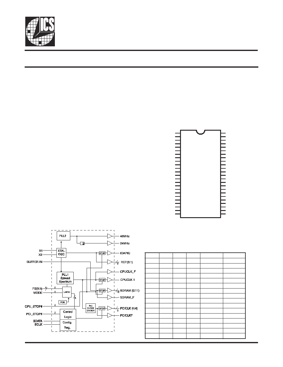
Block Diagram
Frequency Generator & Integrated Buffers for PENTIUM
II
/
III
TM
& K6
Pin Configuration
48-Pin SSOP and TSSOP
* Internal Pull-up Resistor of 120K to VDD
VDDREF
*SPREAD/REF0
GNDREF
X1
X2
VDDPCI
*CPU2.5_3.3#/PCICLK_F
*FS3/PCICLK0
GNDPCI
*SEL24_48#/PCICLK1
*SELPCIE_6#/PCICLK2
PCICLK3
PCICLK4
VDDPCI
BUFFER IN
GNDPCI
PCICLK5
PCICLK6/
VDDCOR
PCI_STOP#
*Vtt_PWRGD/PD#
GND48
SDATA
SCLK
PCICLK_E
REF1/FS2*
VDDLCPU
CPUCLK_F
CPUCLK0
GNDLCPU
CPUCLK1
CPUCLK2
CLK_STOP#
GNDSDR
SDRAM_F
SDRAM0
SDRAM1
VDDSDR
SDRAM2
SDRAM3
GNDSDR
SDRAM4
SDRAM5
VDDSDR
SDRAM6
SDRAM7
VDD48
48MHz/FS0*
24_48MHz/FS1*
ICS9248-195
1
2
3
4
5
6
7
8
9
10
11
12
13
14
15
16
17
18
19
20
21
22
23
24
48
47
46
45
44
43
42
41
40
39
38
37
36
35
34
33
32
31
30
29
28
27
26
25
Recommended Application:
440BX, MX, VIA PM/PL/PLE 133 style chip set, with
Coppermine or Tualatin processor, for note book
applications.
Output Features:
�
4 - CPUs @ 2.5V/3.3V
including 1 free running CPUCLK_F
�
9 - SDRAM @ 3.3V
�
7 - PCI @ 3.3V, including 1 free running PCICLK_F
�
1 - PCI Early @ 3.3V
�
1 - 48MHz, @ 3.3V fixed.
�
1 - 24/48MHz @ 3.3V
�
2 - REF @3.3V, 14.318MHz.
Features:
�
Up to 137MHz frequency support
�
97MHz to support high-end AMD processor.
�
Support power management: CLK, PCI, stop and
Power down Mode from I
2
C programming.
�
Spread spectrum for EMI control
�
Uses external 14.318MHz crystal
�
FS pins for frequency select
Functionality
2
t
i
B
6
t
i
B
5
t
i
B
4
t
i
B
K
L
C
U
P
C
K
L
C
I
C
P
0
0
0
0
7
6
.
6
6
3
3
.
3
3
0
0
0
1
0
0
.
0
0
1
3
3
.
3
3
0
0
1
0
7
6
.
6
6
3
3
.
3
3
0
0
1
1
3
3
.
3
3
1
3
3
.
3
3
0
1
0
0
7
6
.
6
6
3
3
.
3
3
0
1
0
1
0
0
.
0
0
1
3
3
.
3
3
0
1
1
0
0
0
.
0
0
1
3
3
.
3
3
0
1
1
1
3
3
.
3
3
1
3
3
.
3
3
1
0
0
0
7
6
.
6
6
3
3
.
3
3
1
0
0
1
0
0
.
0
0
1
3
3
.
3
3
1
0
1
0
0
0
.
0
9
0
0
.
0
3
1
0
1
1
3
3
.
3
3
1
3
3
.
3
3
1
1
0
0
0
0
.
0
7
0
0
.
5
3
1
1
0
1
0
0
.
5
0
1
0
0
.
5
3
1
1
1
0
3
3
.
3
3
1
3
3
.
3
3
1
1
1
1
0
0
.
0
4
1
0
0
.
5
3
Key Specifications:
�
CPU Output Jitter @ 2.5V: <300ps
�
CPU Output Jitter @ 3.3V: <250ps
�
PCI Output Jitter @ 3.3V: <250ps
�
CPU Output Skew @ 2.5V: <175ps
�
CPU Output Skew @ 3.3V: <175ps
�
PCI Output Skew @ 3.3V: <500ps
�
PCI Early to PCI Skew @ 3.3V: typ = 3ns
�
SDRAM Output Skew @ 3.3V: <500ps

2
ICS9248-195
0375D--02/02/04
Pin Descriptions
Notes:
1:
Internal Pull-up Resistor of 120K to 3.3V on indicated inputs
2:
Bidirectional input/output pins, input logic levels are latched at internal power-on-reset. Use
10Kohm resistor to program logic Hi to VDD or GND for logic low.
N
I
P
R
E
B
M
U
N
E
M
A
N
N
I
P
E
P
Y
T
N
O
I
T
P
I
R
C
S
E
D
1
F
E
R
D
D
V
R
W
P
V
3
.
3
l
a
n
i
m
o
n
,
y
l
p
p
u
s
r
e
w
o
p
L
A
T
X
,
f
e
R
2
D
A
E
R
P
S
2
,
1
N
I
"
n
o
"
s
i
g
n
i
d
a
e
r
p
s
,
"
h
g
i
H
"
s
i
t
l
u
a
f
e
d
p
u
-
r
e
w
o
P
.
t
u
p
n
i
e
l
b
a
n
e
m
u
r
t
c
e
p
S
d
a
e
r
p
S
h
g
i
H
e
v
i
t
c
A
0
F
E
R
T
U
O
s
d
a
o
l
S
U
B
A
S
I
r
o
f
r
e
f
f
u
b
R
E
G
N
O
R
T
S
e
h
t
s
i
t
u
p
t
u
o
F
E
R
s
i
h
T
.
k
c
o
l
c
e
c
n
e
r
e
f
e
r
z
h
M
8
1
3
.
4
1
0
2
#
P
O
T
S
_
I
C
P
N
I
)
0
=
E
D
O
M
,
e
d
o
m
e
li
b
o
m
n
I
(
w
o
l
t
u
p
n
i
n
e
h
w
,
l
e
v
e
l
0
c
i
g
o
l
t
a
s
k
c
o
l
c
K
L
C
I
C
P
s
t
l
a
H
,
6
1
,
9
,
3
4
4
,
0
4
,
3
3
D
N
G
R
W
P
d
n
u
o
r
G
4
1
X
N
I
k
c
a
b
d
e
e
f
d
n
a
)
F
p
6
3
(
p
a
c
d
a
o
l
l
a
n
r
e
t
n
i
s
a
h
,
t
u
p
n
i
l
a
t
s
y
r
C
2
X
m
o
r
f
r
o
t
s
i
s
e
r
5
2
X
T
U
O
.
z
H
M
8
1
3
.
4
1
y
l
l
a
n
i
m
o
n
,
t
u
p
t
u
o
l
a
t
s
y
r
C
4
1
,
6
I
C
P
D
D
V
R
W
P
V
3
.
3
l
a
n
i
m
o
n
K
L
C
I
C
P
d
n
a
F
_
K
L
C
I
C
P
r
o
f
y
l
p
p
u
S
7
#
3
.
3
_
5
.
2
U
P
C
2
,
1
N
I
.
t
u
p
n
I
d
e
h
c
t
a
L
.
U
P
C
V
3
.
3
=
W
O
L
,
U
P
C
V
5
.
2
=
h
g
i
H
.
V
3
.
3
r
o
5
.
2
s
i
U
P
C
L
D
D
V
r
e
h
t
e
h
w
s
e
t
a
c
i
d
n
I
F
_
K
L
C
I
C
P
T
U
O
.
t
n
e
m
e
g
a
n
a
m
r
e
w
o
p
r
o
f
#
P
O
T
S
_
I
C
P
y
b
d
e
t
c
e
f
f
a
t
o
n
k
c
o
l
c
I
C
P
g
n
i
n
n
u
r
e
e
r
F
8
3
S
F
2
,
1
N
I
.
t
u
p
n
I
d
e
h
c
t
a
L
.
n
i
p
t
c
e
l
e
s
y
c
n
e
u
q
e
r
F
0
K
L
C
I
C
P
T
U
O
)
y
l
r
a
e
U
P
C
(
w
e
k
s
s
n
4
-
1
h
t
i
w
s
k
c
o
l
c
U
P
C
o
t
s
u
o
n
o
r
h
c
n
y
S
.
t
u
p
t
u
o
k
c
o
l
c
I
C
P
0
1
#
8
4
_
4
2
L
E
S
2
,
1
N
I
z
H
M
8
4
=
w
o
L
n
e
h
w
z
H
M
8
4
r
o
4
2
r
e
h
t
i
e
s
t
c
e
l
e
S
1
K
L
C
I
C
P
T
U
O
)
y
l
r
a
e
U
P
C
(
w
e
k
s
s
n
4
-
1
h
t
i
w
s
k
c
o
l
c
U
P
C
o
t
s
u
o
n
o
r
h
c
n
y
S
.
t
u
p
t
u
o
k
c
o
l
c
I
C
P
1
1
#
6
_
E
I
C
P
L
E
S
2
,
1
N
I
)
.
K
L
C
I
C
P
y
l
r
a
e
"
h
g
i
H
"
s
i
t
l
u
a
f
e
d
p
u
-
r
e
w
o
p
8
1
n
i
p
r
o
f
(
.
t
u
p
n
i
h
c
t
a
l
t
c
e
l
e
s
I
C
P
l
a
m
r
o
n
r
o
y
l
r
a
E
I
C
P
2
K
L
C
I
C
P
T
U
O
.
t
u
p
t
u
o
k
c
o
l
c
K
L
C
I
C
P
2
1
,
3
1
,
7
1
)
3
:
5
(
K
L
C
I
C
P
T
U
O
)
y
l
r
a
e
U
P
C
(
w
e
k
s
s
n
4
-
1
h
t
i
w
s
k
c
o
l
c
U
P
C
o
t
s
u
o
n
o
r
h
c
n
y
S
.
s
t
u
p
t
u
o
k
c
o
l
c
I
C
P
5
1
N
I
R
E
F
F
U
B
N
I
.
s
t
u
p
t
u
o
M
A
R
D
S
r
o
f
s
r
e
f
f
u
B
t
u
o
n
a
F
o
t
t
u
p
n
I
8
1
-
_
K
L
C
I
C
P
/
6
K
L
C
I
C
P
E
T
U
O
#
6
_
E
I
C
P
L
E
S
y
b
e
l
b
a
t
c
e
l
e
s
t
u
p
t
u
o
k
c
o
l
c
I
C
P
y
l
r
a
e
r
o
t
u
p
t
u
o
k
c
o
l
c
I
C
P
9
1
R
O
C
D
D
V
R
W
P
V
3
.
3
.
e
r
o
c
L
L
P
e
h
t
r
o
f
n
i
p
r
e
w
o
P
1
2
D
N
G
R
W
P
_
t
t
V
N
I
D
G
R
W
P
_
t
t
V
n
e
h
W
.
l
a
n
g
i
s
#
D
P
d
n
a
D
G
R
W
P
_
t
t
V
r
o
f
n
i
p
t
u
p
n
i
n
o
i
t
c
n
u
f
l
a
u
d
a
s
a
s
t
c
a
n
i
p
s
i
h
T
n
a
s
i
n
i
p
e
h
t
r
e
t
f
a
e
r
e
h
t
n
o
r
e
w
o
p
t
a
d
e
h
c
t
a
l
e
b
l
l
i
w
t
c
e
l
e
s
y
c
n
e
u
q
e
r
f
e
h
t
h
g
i
h
s
e
o
g
.
n
i
p
n
w
o
d
r
e
w
o
p
w
o
l
e
v
i
t
c
a
s
u
o
n
o
r
h
c
n
y
s
a
#
D
P
1
N
I
e
h
T
.
e
t
a
t
s
r
e
w
o
p
w
o
l
a
o
t
n
i
e
c
i
v
e
d
e
h
t
n
w
o
d
r
e
w
o
p
o
t
d
e
s
u
n
i
p
t
u
p
n
i
w
o
l
e
v
i
t
c
a
s
u
o
n
o
r
h
c
n
y
s
A
e
h
t
f
o
y
c
n
e
t
a
l
e
h
T
.
d
e
p
p
o
t
s
e
r
a
l
a
t
s
y
r
c
e
h
t
d
n
a
O
C
V
e
h
t
d
n
a
d
e
l
b
a
s
i
d
e
r
a
s
k
c
o
l
c
l
a
n
r
e
t
n
i
.
s
m
4
n
a
h
t
r
e
t
a
e
r
g
e
b
t
o
n
l
l
i
w
n
w
o
d
r
e
w
o
p
2
2
8
4
D
N
G
R
W
P
.
e
r
o
c
L
L
P
d
e
x
i
f
&
s
r
e
f
f
u
b
t
u
p
t
u
o
z
H
M
8
4
&
4
2
e
h
t
r
o
f
n
i
p
d
n
u
o
r
G
,
2
3
,
1
3
,
9
2
,
8
2
8
3
,
7
3
,
5
3
,
4
3
)
0
:
7
(
M
A
R
D
S
T
U
O
.
)
t
e
s
p
i
h
c
y
b
d
e
ll
o
r
t
n
o
c
(
n
i
p
N
I
R
E
F
F
U
B
m
o
r
f
s
t
u
p
t
u
o
r
e
f
f
u
B
t
u
o
n
a
F
,
s
t
u
p
t
u
o
k
c
o
l
c
M
A
R
D
S
6
3
,
0
3
R
D
S
D
D
V
R
W
P
.
V
3
.
3
l
a
n
i
m
o
n
,
e
r
o
C
L
L
P
U
P
C
d
n
a
M
A
R
D
S
r
o
f
y
l
p
p
u
S
3
2
A
T
A
D
S
N
I
I
r
o
f
t
u
p
n
i
a
t
a
D
2
t
u
p
n
i
t
n
a
r
e
l
o
t
V
5
,
t
u
p
n
i
l
a
i
r
e
s
C
4
2
K
L
C
S
N
I
I
f
o
t
u
p
n
i
k
c
o
l
C
2
t
u
p
n
i
t
n
a
r
e
l
o
t
V
5
,
t
u
p
n
i
C
5
2
z
H
M
8
4
_
4
2
T
U
O
0
1
n
i
p
y
b
e
l
b
a
t
c
e
l
e
s
k
c
o
l
c
t
u
p
t
u
o
z
H
M
8
4
r
o
z
H
M
4
2
1
S
F
2
,
1
N
I
.
t
u
p
n
I
d
e
h
c
t
a
L
.
n
i
p
t
c
e
l
e
s
y
c
n
e
u
q
e
r
F
6
2
z
H
M
8
4
T
U
O
k
c
o
l
c
t
u
p
t
u
o
z
H
M
8
4
0
S
F
2
,
1
N
I
t
u
p
n
I
d
e
h
c
t
a
L
.
n
i
p
t
c
e
l
e
s
y
c
n
e
u
q
e
r
F
7
2
8
4
D
D
V
R
W
P
.
e
r
o
c
L
L
P
d
e
x
i
f
d
n
a
s
r
e
f
f
u
b
t
u
p
t
u
o
z
H
M
8
4
&
4
2
r
o
f
r
e
w
o
P
9
3
F
_
M
A
R
D
S
T
U
O
#
P
O
T
S
_
U
P
C
y
b
d
e
t
c
e
f
f
a
t
o
N
.
t
u
p
t
u
o
k
c
o
l
c
M
A
R
D
S
g
n
i
n
n
u
r
e
e
r
F
1
4
#
P
O
T
S
_
K
L
C
N
I
.
w
o
l
n
e
v
i
r
d
n
e
h
w
l
e
v
e
l
"
0
"
c
i
g
o
l
t
a
M
A
R
D
S
&
,
K
L
C
U
P
C
s
t
l
a
h
t
u
p
n
i
s
u
o
n
o
r
h
c
n
y
s
a
s
i
h
T
5
4
,
3
4
,
2
4
)
0
:
2
(
K
L
C
U
P
C
T
U
O
U
P
C
L
D
D
V
y
b
d
e
r
e
w
o
p
,
s
t
u
p
t
u
o
k
c
o
l
c
U
P
C
6
4
F
_
K
L
C
U
P
C
T
U
O
#
P
O
T
S
_
U
P
C
e
h
t
y
b
d
e
t
c
e
f
f
a
t
o
N
.
k
c
o
l
c
U
P
C
g
n
i
n
n
u
r
e
e
r
F
7
4
U
P
C
L
D
D
V
R
W
P
V
5
.
2
s
k
c
o
l
c
U
P
C
r
o
f
y
l
p
p
u
S
8
4
1
F
E
R
T
U
O
.
k
c
o
l
c
e
c
n
e
r
e
f
e
r
z
H
M
8
1
3
.
4
1
2
S
F
2
,
1
N
I
t
u
p
n
I
d
e
h
c
t
a
L
.
n
i
p
t
c
e
l
e
s
y
c
n
e
u
q
e
r
F

3
ICS9248-195
0375D--02/02/04
Byte0: Functionality and Frequency Select Register (default = 0)
Serial Configuration Command Bitmap
Notes:
1, Default at Power-up will be for latched logic inputs to define frequency. Bit [2, 6:4] are default to 0011.
2, PWD = Power-Up Default
The ICS9248-195 is the single chip clock solution for Notebook designs using the 440BX, MX, VIA PM/PL/PLE 133
style chip set, with Coppermine or Tualatin processor, for Note book applications. It provides all necessary clock signals
for such a system.
Spread spectrum may be enabled through I
2
C programming. Spread spectrum typically reduces system EMI by 8dB
to 10dB. This simplifies EMI qualification without resorting to board design iterations or costly shielding. The ICS9248-
195 employs a proprietary closed loop design, which tightly controls the percentage of spreading over process and
temperature variations.
General Description
Bit
PWD
FS3
Bit2
FS2
Bit6
FS1
Bit5
FS0
Bit4
CPUCLK
PCICLK
Center
Spread %
Down
Spread%
0
0
0
0
66.67
33.33
�0.35%
-0.70%
0
0
0
1
100.00
33.33
�0.35%
-0.70%
0
0
1
0
66.67
33.33
�0.60%
-1.20%
0
0
1
1
133.33
33.33
�0.35%
-0.70%
0
1
0
0
66.67
33.33
�0.23%
-0.45%
0
1
0
1
100.00
33.33
�0.23%
-0.45%
0
1
1
0
100.00
33.33
�0.60%
-1.20%
0
1
1
1
133.33
33.33
�0.23%
-0.45%
1
0
0
0
66.67
33.33
�0.45%
-0.90%
1
0
0
1
100.00
33.33
�0.45%
-0.90%
1
0
1
0
90.00
30.00
�0.35%
-0.70%
1
0
1
1
133.33
33.33
�0.45%
-0.90%
1
1
0
0
70.00
35.00
�0.35%
-0.70%
1
1
0
1
105.00
35.00
�0.35%
-0.70%
1
1
1
0
133.33
33.33
�0.60%
-1.20%
1
1
1
1
140.00
35.00
�0.35%
-0.70%
0 - Normal
Note1
0011
Description
1
0
1
0 = Center Spread Spectrum Modulation
1 = Down Spread Spectrum Modulation
0 - Frequency is selected by hardware select pins. Latched inputs.
1 - Frequency is controlled by I
2
C programming.
0 - Running
1 - Tristate all outputs
0
1 - Spread Spectrum Enabled
Bit 0
Bit 7
Bit 3
Bit 2,
6:4
Bit 1

4
ICS9248-195
0375D--02/02/04
Notes:
1. Inactive means outputs are held LOW and are disabled from switching.
2. Latched register values will be inverted from pin values. Default latch condition is for all latched inputs to
be floating (pulled up via internal resistor) at power-up.
Byte 2: Active/Inactive Register (1 = enable, 0 = disable)
t
i
B
#
n
i
P
D
W
P
n
o
i
t
p
i
r
c
s
e
D
7
t
i
B
7
1
)
s
i
D
/
n
E
(
F
_
K
L
C
I
C
P
6
t
i
B
8
1
1
)
s
i
D
/
n
E
(
6
K
L
C
I
C
P
5
t
i
B
7
1
1
)
s
i
D
/
n
E
(
5
K
L
C
I
C
P
4
t
i
B
3
1
1
)
s
i
D
/
n
E
(
4
K
L
C
I
C
P
3
t
i
B
2
1
1
)
s
i
D
/
n
E
(
3
K
L
C
I
C
P
2
t
i
B
1
1
1
)
s
i
D
/
n
E
(
2
K
L
C
I
C
P
1
t
i
B
0
1
1
)
s
i
D
/
n
E
(
1
K
L
C
I
C
P
0
t
i
B
8
1
)
s
i
D
/
n
E
(
0
K
L
C
I
C
P
Byte 1: Active/Inactive Register (1 = enable, 0 = disable)
Byte 3: Active/Inactive Register (1 = enable, 0 = disable)
t
i
B
#
n
i
P
D
W
P
n
o
i
t
p
i
r
c
s
e
D
7
t
i
B
-
1
)
d
e
v
r
e
s
e
R
(
6
t
i
B
6
4
1
)
s
i
D
/
n
E
(
F
_
K
L
C
U
P
C
5
t
i
B
-
0
)
d
e
v
r
e
s
e
R
(
4
t
i
B
-
0
)
d
e
v
r
e
s
e
R
(
3
t
i
B
9
3
1
)
s
i
D
/
n
E
(
F
_
M
A
R
D
S
2
t
i
B
2
4
1
)
s
i
D
/
n
E
(
2
K
L
C
U
P
C
1
t
i
B
3
4
1
)
s
i
D
/
n
E
(
1
K
L
C
U
P
C
0
t
i
B
5
4
1
)
s
i
D
/
n
E
(
0
K
L
C
U
P
C
t
i
B
#
n
i
P
D
W
P
n
o
i
t
p
i
r
c
s
e
D
7
t
i
B
-
1
)
d
e
v
r
e
s
e
R
(
6
t
i
B
-
0
)
d
e
v
r
e
s
e
R
(
5
t
i
B
-
0
)
d
e
v
r
e
s
e
R
(
4
t
i
B
-
0
)
d
e
v
r
e
s
e
R
(
3
t
i
B
8
2
1
)
s
i
D
/
n
E
(
7
M
A
R
D
S
2
t
i
B
9
2
1
)
s
i
D
/
n
E
(
6
M
A
R
D
S
1
t
i
B
1
3
1
)
s
i
D
/
n
E
(
5
M
A
R
D
S
0
t
i
B
2
3
1
)
s
i
D
/
n
E
(
4
M
A
R
D
S

5
ICS9248-195
0375D--02/02/04
Byte 4: Active/Inactive Register (1 = enable, 0 = disable)
Byte 5: Active/Inactive Register (1 = enable, 0 = disable)
Notes:
1. Inactive means outputs are held LOW and are disabled from switching.
2. Latched register values will be inverted from pin values. Default latch condition is for all latched inputs to be floating
(pulled up via internal resistor) at power-up.
t
i
B
#
n
i
P
D
W
P
n
o
i
t
p
i
r
c
s
e
D
7
t
i
B
-
1
)
d
e
v
r
e
s
e
R
(
6
t
i
B
-
0
)
d
e
v
r
e
s
e
R
(
5
t
i
B
-
0
#
)
8
4
_
4
2
L
E
S
(
4
t
i
B
-
0
#
0
S
F
d
e
h
c
t
a
L
3
t
i
B
-
0
#
1
S
F
d
e
h
c
t
a
L
2
t
i
B
-
0
#
2
S
F
d
e
h
c
t
a
L
1
t
i
B
-
0
#
3
S
F
d
e
h
c
t
a
L
0
t
i
B
-
1
)
d
e
v
r
e
s
e
R
(
t
i
B
#
n
i
P
D
W
P
n
o
i
t
p
i
r
c
s
e
D
7
t
i
B
4
3
1
)
s
i
D
/
n
E
(
3
M
A
R
D
S
6
t
i
B
5
3
1
)
s
i
D
/
n
E
(
2
M
A
R
D
S
5
t
i
B
7
3
1
)
s
i
D
/
n
E
(
1
M
A
R
D
S
4
t
i
B
8
3
1
)
s
i
D
/
n
E
(
0
M
A
R
D
S
3
t
i
B
6
2
1
)
s
i
D
/
n
E
(
z
H
M
8
4
2
t
i
B
5
2
1
)
s
i
D
/
n
E
(
z
H
M
4
2
1
t
i
B
8
4
1
)
s
i
D
/
n
E
(
1
F
E
R
0
t
i
B
2
1
)
s
i
D
/
n
E
(
0
F
E
R