Äîêóìåíòàöèÿ è îïèñàíèÿ www.docs.chipfind.ru

Integrated
Circuit
Systems, Inc.
ICS9248-65
Third party brands and names are the property of their respective owners.
Block Diagram
Frequency Timing Generator for PENTIUM II
Systems
9248-65 Rev C 7/28/99
Pin Configuration
48-pin SSOP
Generates the following system clocks:
- 3 CPU clocks ( 2.5V, 100/133MHz)
- 10 PCI clocks, including 1 free-running
(3.3V, 33.3MHz)
- 1 CPU/2 clocks (2.5V, 50/66.6MHz)
- 1 IOAPIC clocks (2.5V, 16.67MHz)
- 3 Fixed frequency 66MHz clocks(3.3V, 66.6MHz)
- 2 REF clocks(3.3V, 14.318MHz)
- 1 USB clock (3.3V, 48MHz)
Efficient power management through PD#.
0 to -0.5% typical down spread modulation on CPU, PCI,
IOAPIC, 3V66 and CPU/2 output clocks.
Uses external 14.318MHz crystal.
ICS reserves the right to make changes in the device data identified in
this publication without further notice. ICS advises its customers to
obtain the latest version of all device data to verify that any
information being relied upon by the customer is current and accurate.
Features
Key Specification
CPU Output Jitter: <250ps
CPU/2 Output Jitter. <250ps
IOAPIC Output Jitter: <500ps
48MHz, 3V66, PCI Output Jitter: <500ps
PCI Output Jitter. <500ps
Ref Output Jitter. <1000ps
CPU 0:2 Output Skew: <175ps
PCI_F, PCI 1:7 Output Skew: <500ps
3V66_0:2 Output Skew <250ps
CPU to 3V66_0:2 Output Offset: 0.0 - 1.5ns (CPU leads)
3V66 to PCI Output Offset: 1.5 - 4ns (CPU leads)
CPU to IOAPIC Output Offset 1.5 - 4.0ns (CPU leads)
2
ICS9248-65
Pin Descriptions
Pin number Pin name
Type
Description
1,2
REF
Output
3.3V, 14.318 MHz reference clock output.
3, 9, 17, 24,
28, 34
VDD
Power
3.3 V power for clock outputs.
4
X1
Input
14.318 MHz crystal input
5
X2
Output
14.318 MHz crystal output
6,14, 20, 26,
33, 45, 48
GND
Power
Ground for clock outputs
7
PCICLK_F
Output
3.3 V free running PCI clock output, will not be stopped by the PCI_STOP#
8,10,11,12,13,
15,16,18,19
PCICLK (1:9)
Output
3.3 V PCI clock outputs, generating timing requirements for
21,22,23
3V66
Output
3.3 V 66 MHz clock output, fixed frequency clock typically used with AGP
25
SEL
133/100#
Input
Control for the frequency of clocks at the CPU output pins. If logic "0" is used the
100 MHz frequency is selected. If Logic "1" is used, the 133 MHz frequency is
selected. The PCI clock is multiplexed to run at 33.3 MHz for both selected cases.
27
48 MHz
Output
3.3 V 48 MHz clock output, fixed frequency clock typically used with USB
devices
29,30
SEL (0:1)
Input
Frequency select pin , logic input.
31
SPREAD#
Output
Power-on spread spectrum enable option. Active low = spread spectrum clocking
enable. Active high = spread spectrum clocking disable.
32
PD#
Input
Asynchronous active low input pin used to power down the device into a low
power state. The internal clocks are disabled and the VCO and the crystal are
stopped.
35,39
GNDLCPU
Power
Ground for the CPU and Host clock outputs
36,37,40
CPUCLK
(0:2)
0utput
2.5 V CPU and Host clock outputs
38,41
VDDLCPU
Power
2.5 V power for the CPU and Host clock outputs
42
GNDLCPU/2
Power
Ground for the CPU and Host clock outputs
43
CPU/2
Output
Output running at 1/2 CPU clock frequency.Synchronous to the CPU outputs.
44
VDDLCPU/2
Power
2.5 V power for the CPU/2 clock outputs
46
IOAPIC(0:1)
Output
2.5V fixed 16.6 MHz IOAPIC clock outputs
47
VDDIOAPIC
Power
2.5V power for IOAPIC clock
The ICS9248-65 is a main clock synthesizer chip for Pentium
II based systems using Rambus Interface DRAMs. This chip
provides all the clocks required for such a system when used
with a Direct Rambus Clock Generator(DRCG) chip such as
the ICS9211-01.
Spread Spectrum may be enabled by driving the SPREAD#
pin active. Spread spectrum typically reduces system EMI by
8dB to 10dB. This simplifies EMI qualification without
resorting to board design iterations or costly shielding. The
ICS9248-65 employs a proprietary closed loop design, which
tightly controls the percentage of spreading over process
and temperature variations.
The CPU/2 clocks are inputs to the DRCG.
General Description
Power Groups:
VDDREF, GNDREF = REF, X1, X2
GNDPCI, VDDPCI = PCICLK
VDD66, GND66 = 3V66
VDD48, GND48 = 48MHz
VDDCOR, GNDCOR = PLL Core
VDDLCPU/2 , GNDLCPU/2 = CPU/2
VDDLIOAPIC, GNDIOAPIC = IOAPIC

3
ICS9248-65
Frequency Select:
Note:
1. TCLK is a test clock driven on the x1 input during test mode.
ICS9248-65 Power Management Features:
Note:
1. LOW means outputs held static LOW as per latency requirement next page.
2. On means active.
3. PD# pulled Low, impacts all outputs including REF and 48 MHz outputs.
L
E
S
#
0
0
1
/
3
3
1
1
L
E
S
0
L
E
S
U
P
C
z
H
M
2
/
U
P
C
z
H
M
6
6
V
3
z
H
M
I
C
P
z
H
M
8
4
z
H
M
F
E
R
z
H
M
C
I
P
A
O
I
z
H
M
s
t
n
e
m
m
o
C
0
0
0
Z
-
i
H
Z
-
i
H
Z
-
i
H
Z
-
i
H
Z
-
i
H
Z
-
i
H
Z
-
i
H
e
t
a
t
s
-
i
r
T
0
0
1
A
/
N
A
/
N
A
/
N
A
/
N
A
/
N
A
/
N
A
/
N
d
e
v
r
e
s
e
R
0
1
0
0
0
1
0
5
6
.
6
6
3
.
3
3
Z
-
i
H
8
1
3
.
4
1
7
6
.
6
1
L
L
P
z
H
M
8
4
d
e
l
b
a
s
i
d
0
1
1
0
0
1
0
5
6
.
6
6
3
.
3
3
8
4
8
1
3
.
4
1
7
6
.
6
1
1
0
0
2
/
K
L
C
T
4
/
K
L
C
T
4
/
K
L
C
T
8
/
K
L
C
T
2
/
K
L
C
T
K
L
C
T
6
1
/
K
L
C
T
)
1
(
e
d
o
m
t
s
e
T
1
0
1
A
/
N
A
/
N
A
/
N
A
/
N
A
/
N
A
/
N
A
/
N
d
e
v
r
e
s
e
R
1
1
0
3
.
3
3
1
6
6
6
6
3
3
Z
-
i
H
8
1
3
.
4
1
7
6
.
6
1
1
1
1
3
.
3
3
1
6
6
6
6
3
3
8
4
8
1
3
.
4
1
7
6
.
6
1
#
D
P
K
L
C
U
P
C
2
/
U
P
C
C
I
P
A
O
I
6
6
V
3
I
C
P
F
_
I
C
P
.
F
E
R
z
H
M
8
4
c
s
O
s
O
C
V
0
W
O
L
W
O
L
W
O
L
W
O
L
W
O
L
W
O
L
W
O
L
F
F
O
F
F
O
1
N
O
N
O
N
O
N
O
N
O
N
O
N
O
N
O
N
O
Power Management Requirements:
Note:
1. Clock on/off latency is defined in the number of rising edges of free running PCICLKs between the clock disable goes low/
high to the first valid clock comes out of the device.
2. Power up latency is when PWR_DWN# goes inactive (high to when the first valid clocks are dirven from the device.
l
a
g
n
i
S
e
t
a
t
S
l
a
g
n
i
S
y
c
n
e
t
a
L
s
e
g
d
e
g
n
i
si
r
f
o
.
o
N
K
L
C
I
C
P
f
o
#
D
P
)
n
o
it
a
r
e
p
o
l
a
m
r
o
n
(
1
S
m
3
)
n
w
o
d
r
e
w
o
p
(
0
.
x
a
m
2
4
ICS9248-65
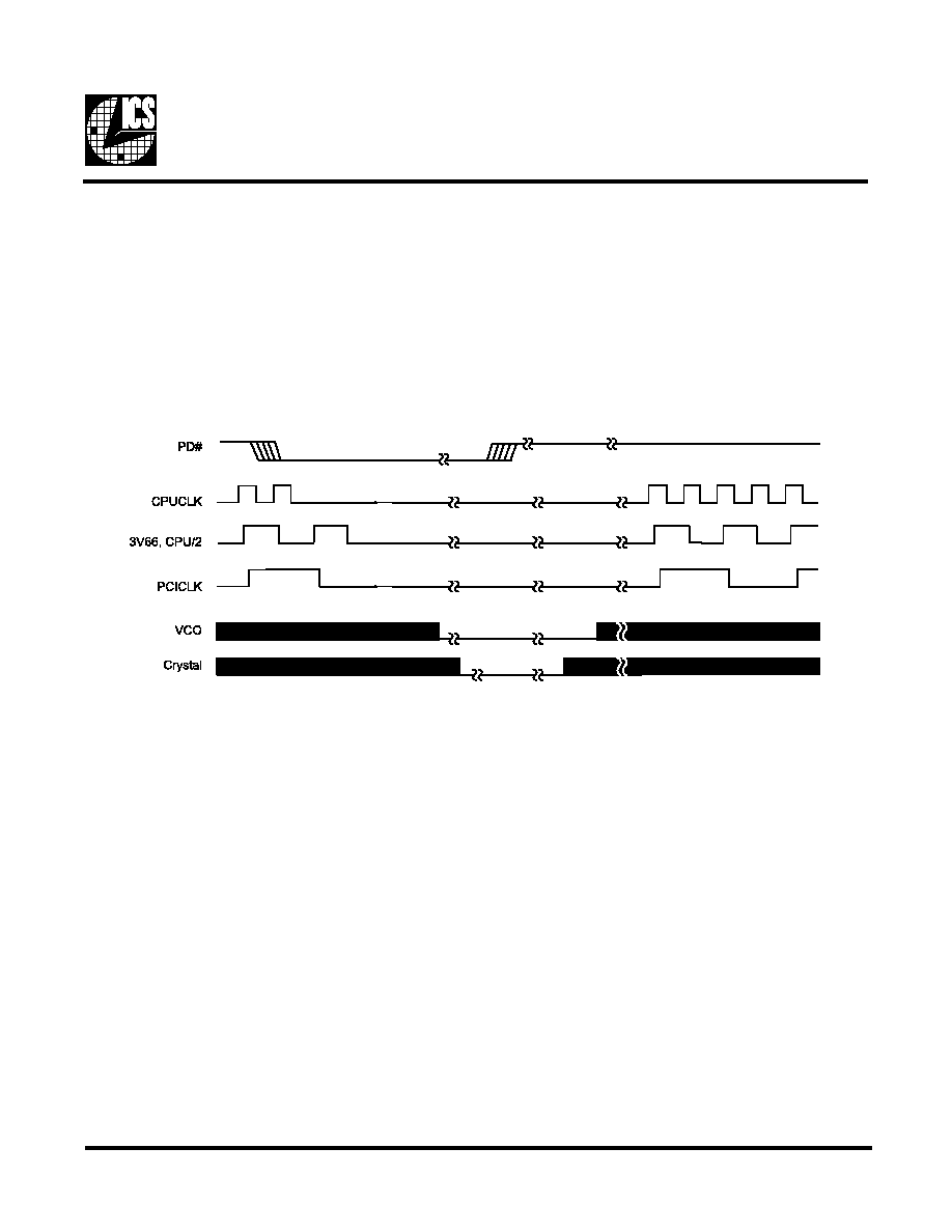
PD# Timing Diagram
The power down selection is used to put the part into a very low power state without turning off the power to the part. PD# is
an asynchronous active low input. This signal needs to be synchronized internal to the device prior to powering down the clock
synthesizer.
Internal clocks are not running after the device is put in power down. When PD# is active low all clocks need to be driven to a
low value and held prior to turning off the VCOs and crystal. The power up latency needs to be less than 3 mS. The power down
latency should be as short as possible but conforming to the sequence requirements shown below. PCI_STOP# and CPU_STOP#
are considered to be don't cares during the power down operations. The REF and 48MHz clocks are expected to be stopped in
the LOW state as soon as possible. Due to the state of the internal logic, stopping and holding the REF clock outputs in the
LOW state may require more than one clock cycle to complete.
Notes:
1. All timing is referenced to the Internal CPUCLK (defined as inside the ICS9248 device).
2. As shown, the outputs Stop Low on the next falling edge after PD# goes low.
3. PD# is an asynchronous input and metastable conditions may exist. This signal is synchronized inside this part.
4. The shaded sections on the VCO and the Crystal signals indicate an active clock.
5. Diagrams shown with respect to 133MHz. Similar operation when CPU is 100MHz.
5
ICS9248-65
Absolute Maximum Ratings
Supply Voltage . . . . . . . . . . . . . . . . . . . . . . . . . . . 7.0 V
Logic Inputs . . . . . . . . . . . . . . . . . . . . . . . . . . . . GND 0.5 V to V
DD
+0.5 V
Ambient Operating Temperature . . . . . . . . . . . . 0°C to +70°C
Storage Temperature . . . . . . . . . . . . . . . . . . . . . . 65°C to +150°C
Stresses above those listed under Absolute Maximum Ratings may cause permanent damage to the device. These ratings are
stress specifications only and functional operation of the device at these or any other conditions above those listed in the
operational sections of the specifications is not implied. Exposure to absolute maximum rating conditions for extended periods
may affect product reliability.
Electrical Characteristics - Input/Supply/Common Output Parameters
T
A
= 0 - 70º C; Supply Voltage V
DD
= VDDL = 3.3 V +/-5%, (unless otherwise stated)
PARAMETER
SYMBOL
CONDITIONS
MIN
TYP
MAX
UNITS
Input High Voltage
V
IH
2
V
DD
+0.3
V
Input Low Voltage
V
IL
V
SS
-0.3
0.8
V
Input High Current
I
IH
V
IN
= V
DD
0.1
5
µ
A
Input Low Current
I
IL1
V
IN
= 0 V; Inputs with no pull-up resistors
-5
2.0
µ
A
Input Low Current
I
IL2
V
IN
= 0 V; Inputs with pull-up resistors
-200
-100
µ
A
I
DD3.3OP 100
C
L
= 0 pF; Select @ 100 MHz
65
I
DD3.3OP 133
C
L
= 0 pF; Select @ 133.3 MHz
71
I
DD3.3OP 144
C
L
= 0 pF; Select @ 144 MHz
75
I
DD3.3OP 154
C
L
= 0 pF; Select @ 154 MHz
78
Power Down
I
DD3.3P D
C
L
= 0 pF; PWRDWN# = 0
64
200
µ
A
Supply Current
Input frequency
F
i
V
DD
= 3.3 V
12
14.318
16
MHz
Input Capacitance
1
C
IN
Logic Inputs
5
pF
C
INX
X1 & X2 pins
27
36
45
pF
Transition Time
1
T
trans
To 1st crossing of target Freq.
1
3
ms
Settling Time
1
T
s
From 1st crossing to 1% target Freq.
0.5
ms
Clk Stabilization
1
T
STAB
From V
DD
= 3.3 V to 1% target Freq.
3
ms
Skew
1
t
CP U-P CI
V
T
= 1.5 V; V
TL
= 1.25 V
1.5
2.4
4
ns
Skew
1
t
CP U-3V66
V
T
= 1.5 V; V
TL
= 1.25 V
1.4
1.5
ns
Skew
1
t
3V66-P CI
V
T
= 1.5 V
1.4
4
ns
1
Guaranteed by design, not 100% tested in production.
Operating
160
mA
Group Offset
Group
Offset
Measurement L oads
Measure Points
CPU to 3V66
0.0-1.5ns CPU leads
C PU @ 20pF, 3V66 @ 30pF
CPU @1.25V, 3V66 @ 1.5V
3V66 to PCI
1.5-4.0ns 3V66 leads
3V66 @ 30pF, PCI @ 30pF
3V66 @ 1.5V, PC I @ 1.5V
CPU to IOAPIC
1.5-4.0ns CPU leads
CPU @ 20pF, IOAPIC @ 20pF
CPU @1.25V, IOAPIC @ 1.5V
No te: 1 . All o ffsets are to be meas u red at ris in g edg es.