Äîêóìåíòàöèÿ è îïèñàíèÿ www.docs.chipfind.ru
Integrated
Circuit
Systems, Inc.
General Description
Features
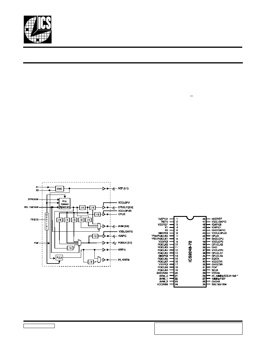
ICS9248-72
Block Diagram
Frequency Timing Generator for PENTIUM II Systems
9248-72 Rev B 7/28/99
Pin Configuration
48-pin SSOP
Up to 200MHz frequency support.
Power Down feature.
Spread Spectrum for EMI control
(0 to 0.5% down spread , + 0.25% center spread)
I
2
C interface.
VDDL=2.5V,VDD=3.3V
The ICS9248-72 is a main clock synthesizer chip for Pentium
II based systems using Rambus Interface DRAMs. This chip
provides all the clocks required for such a system when used
with a Direct Rambus Clock Generator(DRCG) chip such as
the ICS9211-01.
Spread Spectrum may be enabled by driving the SPREAD#
pin active. Spread spectrum typically reduces system EMI by
8dB to 10dB. This simplifies EMI qualification without resorting
to board design iterations or costly shielding. The ICS9248-
72 employs a proprietary closed loop design, which tightly
controls the percentage of spreading over process and
temperature variations.
The CPU/2 clocks are inputs to the DRCG.
Preliminary Product Preview
* 250K ohm pull-up to VDD on indicated inputs.
1.These pins will have 2X drive strength
Key Specification
CPU Output Jitter: <250ps
CPU/2 Output Jitter. <250ps
IOAPIC Output Jitter: <500ps
48MHz, 3V66, PCI Output Jitter: <500ps
Ref Output Jitter. <1000ps
CPU Output Skew: <175ps
IOAPIC Output Skew <250ps
PCI Output Skew: <500ps
3V66 Output Skew <250ps
CPU to 3V66 Output Offset: 0.0 - 1.5ns (CPU leads)
3V66 to PCI Output Offset: 1.5 - 4.0ns (3V66 leads)
CPU to IOAPIC Output Offset 1.5 - 4.0ns (CPU leads)
PRODUCT PREVIEW documents contain information on new
products in the sampling or preproduction phase of development.
Characteristic data and other specifications are subject to change
without notice.
2
ICS9248-72
Preliminary Product Preview
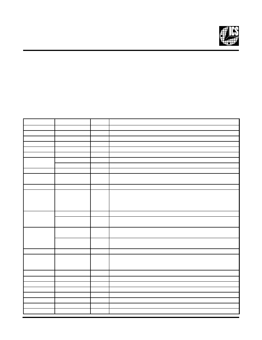
Pin Descriptions
Pin number
Pin name
Type
Description
1, 45, 46
IOAPIC[2:0]
Output
2.5V IOAPIC clock outputs
2
REF0
Output
3.3V, 14.318 MHz reference clock output.
3, 24, 29, 33
VDD
Power
3.3 V power
4
X1
Input
14.318 MHz crystal input
5
X2
Output
14.318 MHz crystal output
6, 14, 20, 26, 32
GND
Power
Ground
FS [2:1]
IN
Frequency select pins. Latched Inputs determins the CPU & PCI frequencies.
PCICLK [1:0]
Output
3.3 V PCI clock outputs, generating timing requirements for
9,17
VDDPCI
Power
3.3 V power for the PCI clock outputs
19, 18, 16, 15, 13,
12, 11, 10
PCICLK [9:2]
Output
3.3 V PCI clock outputs
23, 22, 21
3V66
Output
3.3 V 66 MHz clock output, fixed frequency clock typically used with AGP
25
SEL 133/100#
Input
control for the frequency of clocks at the CPU output pins. If logic "0" is used the
100 MHz frequency is selected. If Logic "1" is used, the 133 MHz frequency is
selected. The PCI clock is multiplexed to run at 33.3 MHz for both selected cases.
FS0
IN
Frequency select pin. Latched Inputs determins the CPU & PCI frequencies.
48 MHz
Output
3.3 V 48 MHz clock output, fixed frequency clock typically used with USB
devices
SEL24/48
IN
48/24 MHz select option. Active low = 48 MHz output. Active High = 24
MHz
24_48MHz#
Output
3.3V 48 or 24 MHz clock output, fixed frequency clock typically used with
USB devices.
30
SCLK
IN
Clock input of I2C input
31
PD#
Input
Asynchronous active low input pin used to power down the device into a low
power state. The internal clocks are disabled and the VCO and the crystal are
stopped.
34
SDATA
IN
Data input for I
2
C serial input.
36, 35
CPUCLK [1:0]
0utput
2.5 V CPU and Host clock outputs
37, 40
VDDLCPU
Power
2.5 V power for the CPU and Host clock outputs
41
GNDLCPU/2
Power
Ground for the CPU and Host clock outputs
42
CPU/2
Output
output running at 1/2 CPU clock frequency.Synchronous to the CPU outputs.
43
VDDLCPU/2
Power
2.5 V power for the CPU/2 clock outputs
47
GNDLIOAPIC
Power
Ground for IOAPIC clocks
48
GNDREF
Power
Ground for 14.318 MHz reference clock outputs
8, 7
28
27
Power Groups:
VDDREF, GNDREF = REF, X1, X2
GNDPCI, VDDPCI = PCICLK
VDD66, GND66 = 3V66
VDD48, GND48 = 48MHz
VDDCOR, GNDCOR = PLL Core
VDDLCPU/2 , GNDLCPU/2 = CPU/2
VDDLIOAPIC, GNDIOAPIC = IOAPIC
3
ICS9248-72
Preliminary Product Preview
ICS9248-72 Power Management Features:
Note:
1. LOW means outputs held static LOW as per latency requirement next page.
2. On means active.
3. PD# pulled Low, impacts all outputs including REF and 48 MHz outputs.
#
D
P
K
L
C
U
P
C
2
/
U
P
C
C
I
P
A
O
I
6
6
V
3
I
C
P
F
_
I
C
P
.
F
E
R
z
H
M
8
4
c
s
O
s
O
C
V
0
W
O
L
W
O
L
W
O
L
W
O
L
W
O
L
W
O
L
W
O
L
F
F
O
F
F
O
1
N
O
N
O
N
O
N
O
N
O
N
O
N
O
N
O
N
O
Power Management Requirements:
Note:
1. Clock on/off latency is defined in the number of rising edges of free running PCICLKs between the clock disable goes low/
high to the first valid clock comes out of the device.
2. Power up latency is when PWR_DWN# goes inactive (high to when the first valid clocks are dirven from the device.
l
a
g
n
i
S
e
t
a
t
S
l
a
g
n
i
S
y
c
n
e
t
a
L
s
e
g
d
e
g
n
i
s
i
r
f
o
.
o
N
K
L
C
I
C
P
f
o
#
D
P
)
n
o
i
t
a
r
e
p
o
l
a
m
r
o
n
(
1
S
m
3
)
n
w
o
d
r
e
w
o
p
(
0
.
x
a
m
2
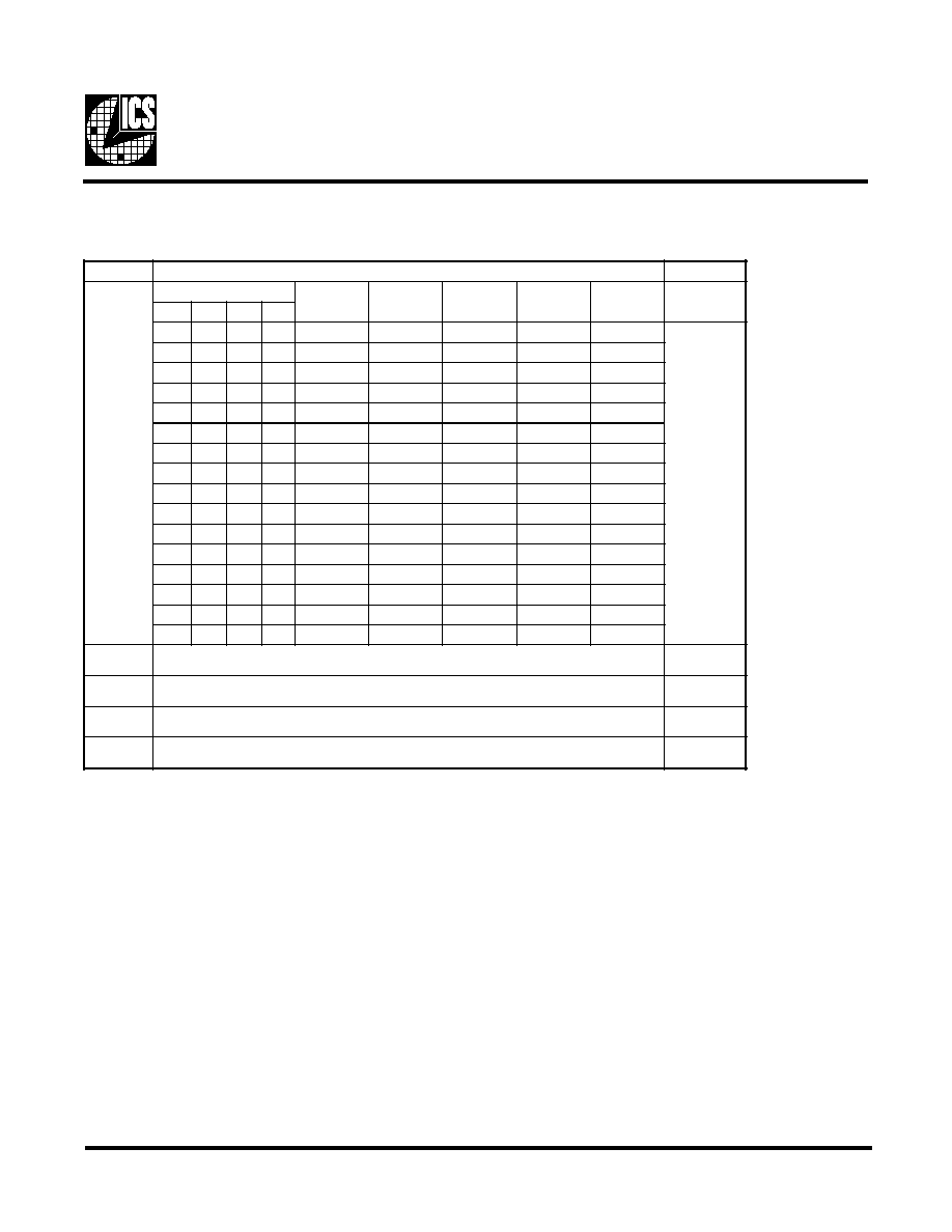
Functionality
V
DD
= 3.3V±5%, V
DDL
= 2.5V ±5% TA= 0 to 70°C
Crystal (X1, X2) = 14.31818MHz
SEL133/100#
FS2
(MHz)
FS1
(MHz)
FS0
(MHz)
CPU
(MHz)
CPU/2
(MHz)
PCI
(MHz)
3V66
(MHz)
IOAPIC
(MHz)
1
1
1
1
133.30
66.65
33.325
66.65
16.66
1
1
1
0
138.01
69.01
34.505
69.01
17.25
1
1
0
1
142.91
71.45
35.725
71.45
17.86
1
1
0
0
147.95
73.98
36.99
73.98
18.49
1
0
1
1
152.49
76.24
38.12
76.24
19.06
1
0
1
0
156.99
78.49
39.245
78.49
19.62
1
0
0
1
162.02
81.01
40.505
81.01
20.25
1
0
0
0
180.00
89.99
30.00
60.00
15.00
0
1
1
1
100.23
50.11
33.405
66.81
16.70
0
1
1
0
105.00
52.49
35
70.00
17.50
0
1
0
1
113.99
56.99
37.83
75.66
18.91
0
1
0
0
120.00
59.99
40.00
80.00
20.00
0
0
1
1
128.51
64.25
32.125
64.25
16.06
0
0
1
0
200.01
100.00
33.33
66.66
16.66
0
0
0
1
170.03
85.01
28.33
56.66
14.16
0
0
0
0
66.82
33.40
33.40
66.80
16.7
4
ICS9248-72
Preliminary Product Preview
1.
The ICS clock generator is a slave/receiver, I
2
C component. It can read back the data stored in the latches for verification.
Read-Back will support Intel PIIX4 "Block-Read" protocol.
2.
The data transfer rate supported by this clock generator is 100K bits/sec or less (standard mode)
3.
The input is operating at 3.3V logic levels.
4.
The data byte format is 8 bit bytes.
5.
To simplify the clock generator I
2
C interface, the protocol is set to use only "Block-Writes" from the controller. The
bytes must be accessed in sequential order from lowest to highest byte with the ability to stop after any complete byte
has been transferred. The Command code and Byte count shown above must be sent, but the data is ignored for those
two bytes. The data is loaded until a Stop sequence is issued.
6.
At power-on, all registers are set to a default condition, as shown.
General I
2
C serial interface information
The information in this section assumes familiarity with I
2
C programming.
For more information, contact ICS for an I
2
C programming application note.
How to Write:
Controller (host) sends a start bit.
Controller (host) sends the write address D2
(H)
ICS clock will acknowledge
Controller (host) sends a dummy command code
ICS clock will acknowledge
Controller (host) sends a dummy byte count
ICS clock will acknowledge
Controller (host) starts sending first byte (Byte 0)
through byte 5
ICS clock will acknowledge each byte one at a time.
Controller (host) sends a Stop bit
How to Read:
Controller (host) will send start bit.
Controller (host) sends the read address D3
(H)
ICS clock will acknowledge
ICS clock will send the byte count
Controller (host) acknowledges
ICS clock sends first byte (Byte 0) through byte 5
Controller (host) will need to acknowledge each byte
Controller (host) will send a stop bit
Notes:
Controller (Host)
ICS (Slave/Receiver)
Start Bit
Address
D3
(H)
ACK
Byte Count
ACK
Byte 0
ACK
Byte 1
ACK
Byte 2
ACK
Byte 3
ACK
Byte 4
ACK
Byte 5
ACK
Stop Bit
How to Read:
Controller (Host)
ICS (Slave/Receiver)
Start Bit
Address
D2
(H)
ACK
Dummy Command Code
ACK
Dummy Byte Count
ACK
Byte 0
ACK
Byte 1
ACK
Byte 2
ACK
Byte 3
ACK
Byte 4
ACK
Byte 5
ACK
Stop Bit
How to Write:
5
ICS9248-72
Preliminary Product Preview
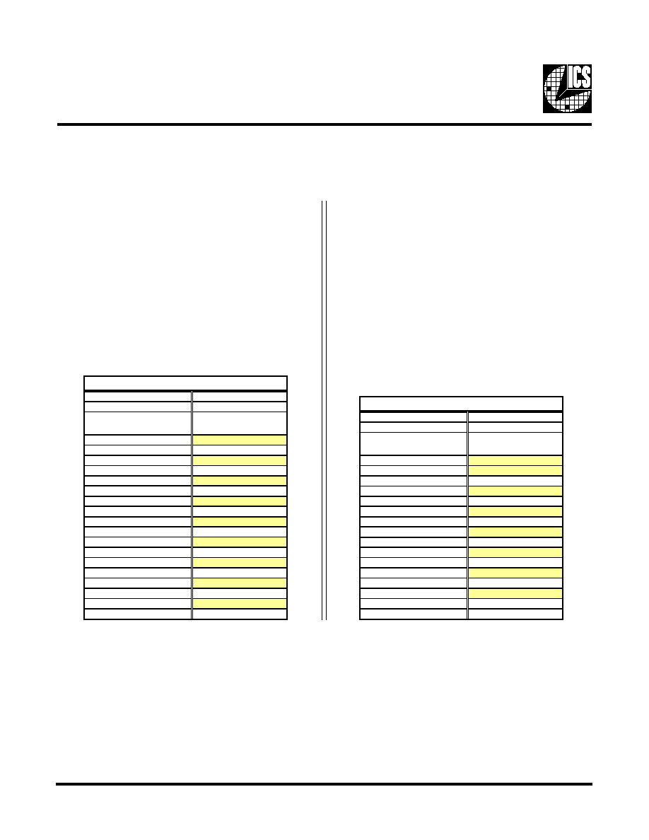
Byte0: Functionality and Frequency Select Register (default = 0)
Serial Configuration Command Bitmap
Note1: Default at power-up will be for latched logic inputs to define frequency.
t
i
B
n
o
i
t
p
i
r
c
s
e
D
D
W
P
t
i
B
)
4
:
7
(
t
i
B
K
L
C
U
P
C
2
/
U
P
C
6
6
V
3
K
L
C
I
C
P
C
I
P
A
O
I
0
7
6
5
4
1
1
1
1
0
3
.
3
3
1
5
6
.
6
6
5
6
.
6
6
5
2
3
.
3
3
6
6
.
6
1
X
X
X
X
1
e
t
o
N
1
1
1
0
1
0
.
8
3
1
1
0
.
9
6
1
0
.
9
6
5
0
5
.
4
3
5
2
.
7
1
1
1
0
1
1
9
.
2
4
1
5
4
.
1
7
5
4
.
1
7
5
2
7
.
5
3
6
8
.
7
1
1
1
0
0
5
9
.
7
4
1
8
9
.
3
7
8
9
.
3
7
9
9
.
6
3
9
4
.
8
1
1
0
1
1
9
4
.
2
5
1
4
2
.
6
7
4
2
.
6
7
2
1
.
8
3
6
0
.
9
1
1
0
1
0
9
9
.
6
5
1
9
4
.
8
7
9
4
.
8
7
5
4
2
.
9
3
2
6
.
9
1
1
0
0
1
2
0
.
2
6
1
1
0
.
1
8
1
0
.
1
8
5
0
5
.
0
4
5
2
.
0
2
1
0
0
0
0
0
.
0
8
1
9
9
.
9
8
0
0
.
0
6
0
0
.
0
3
0
0
.
5
1
0
1
1
1
3
2
.
0
0
1
1
1
.
0
5
1
8
.
6
6
5
0
4
.
3
3
0
7
.
6
1
0
1
1
0
0
0
.
5
0
1
9
4
.
2
5
0
0
.
0
7
5
3
0
5
.
7
1
0
1
0
1
9
9
.
3
1
1
9
9
.
6
5
6
6
.
5
7
3
8
.
7
3
1
9
.
8
1
0
1
0
0
0
0
.
0
2
1
9
9
.
9
5
0
0
.
0
8
0
0
.
0
4
0
0
.
0
2
0
0
1
1
1
5
.
8
2
1
5
2
.
4
6
5
2
.
4
6
5
2
1
.
2
3
6
0
.
6
1
0
0
1
0
1
0
.
0
0
2
0
0
.
0
0
1
6
6
.
6
6
3
3
.
3
3
6
6
.
6
1
0
0
0
1
3
0
.
0
7
1
1
0
.
5
8
6
6
.
6
5
3
3
.
8
2
6
1
.
4
1
0
0
0
0
2
8
.
6
6
0
4
.
3
3
0
8
.
6
6
0
4
.
3
3
7
.
6
1
3
t
i
B
s
t
u
p
n
i
d
e
h
c
t
a
l
,
t
c
e
l
e
s
e
r
a
w
d
r
a
h
y
b
d
e
t
c
e
l
e
s
s
i
y
c
n
e
u
q
e
r
F
-
0
4
:
7
t
i
B
y
b
d
e
t
c
e
l
e
s
s
i
y
c
n
e
u
q
e
r
F
-
1
0
2
t
i
B
%
5
2
.
0
±
e
p
y
t
d
a
e
r
p
s
r
e
t
n
e
c
m
u
r
t
c
e
p
s
d
a
e
r
p
S
-
0
%
5
.
0
-
o
t
0
e
p
y
t
d
a
e
r
p
s
n
w
o
d
m
u
r
t
c
e
p
s
d
a
e
r
p
S
-
1
1
1
t
i
B
l
a
m
r
o
N
-
0
e
l
b
a
n
e
m
u
r
t
c
e
p
s
d
a
e
r
p
S
-
1
1
0
t
i
B
g
n
i
n
n
u
R
=
0
s
t
u
p
t
u
o
l
l
a
e
t
a
t
s
i
r
T
=
1
0