Integrated
Circuit
Systems, Inc.
Features
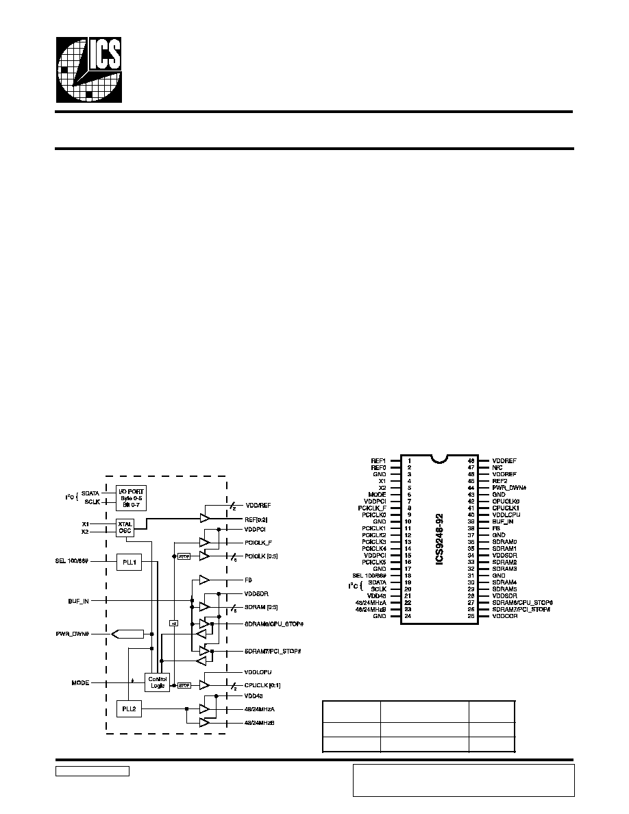
ICS9248-92
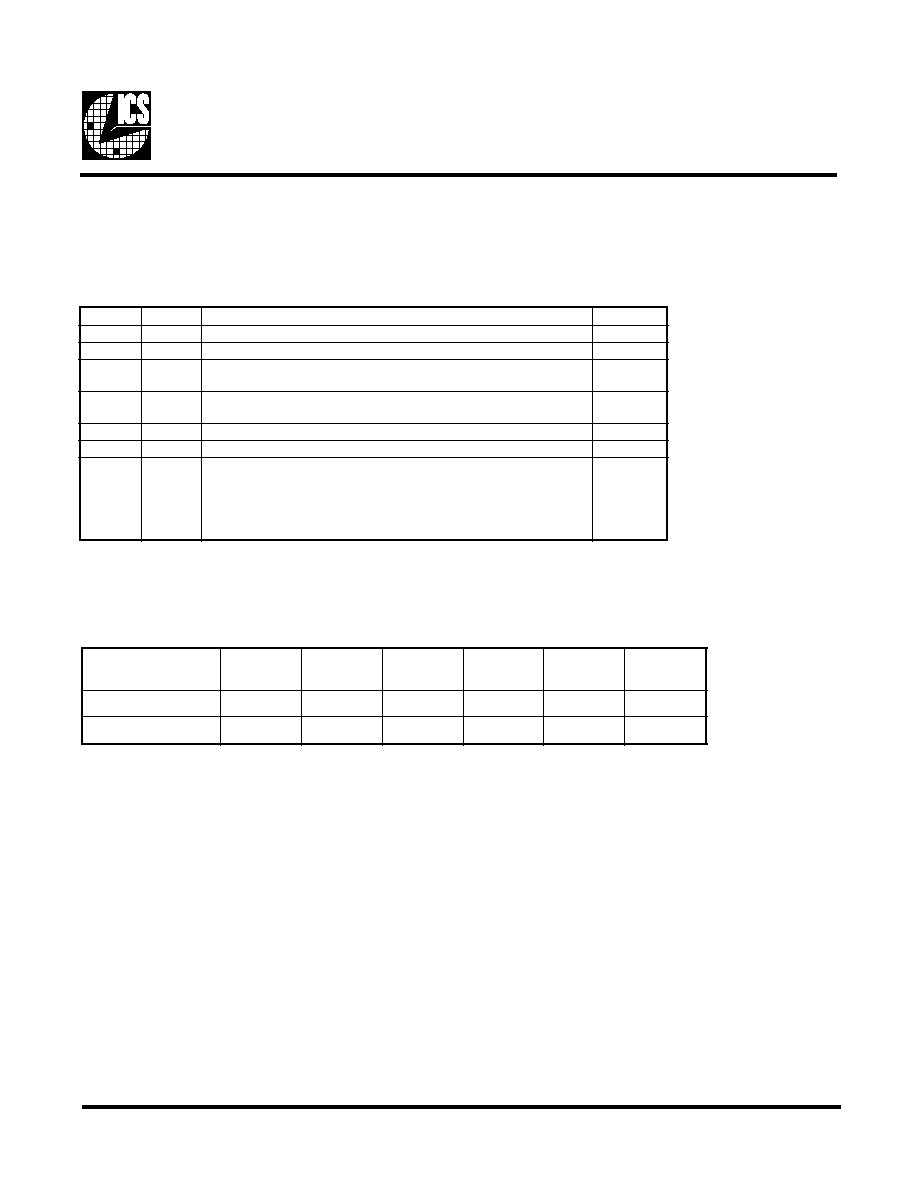
Block Diagram
Mobile Pentium II
TM
System Clock Chip
9248-92 Rev E 02/21/01
Pentium is a trademark on Intel Corporation.
·
Generates system clocks for CPU, SDRAM, PCI, plus
14.318 MHz REF(0:2), USB, Plus Super I/O
·
I
2
C serial configuration interface provides output clock
disabling and other functions
·
MODE input pin selects optional power management
input control pins
·
Two fixed outputs separately selectable as 24 or 48MHz
·
2.5V outputs: CPU
·
3.3V outputs: SDRAM, PCI, REF, 48/24 MHz
·
No power supply sequence requirements
·
Uses external 14.318MHz crystal
·
48 pin 240 mil TSSOP package
·
Output enable register
for serial port control:
1 = enable
0 = disable
General Description:
Features include two strong CPU, seven PCI and eight SDRAM
clocks. Three reference outputs are available equal to the
crystal frequency. Stronger drive CPUCLK outputs typically
provide greater than 1 V/ns slew rate into 20pF loads. This
device meets rise and fall requirements with 2 loads per CPU
output (ie, one clock to CPU and NB chipset, one clock to two
L2 cache inputs).
PWR_DWN# pin allows low power mode by stopping crystal
OSC and PLL stages. For optional power management,
CPU_STOP# can stop CPU (0:1) clocks and PCI_STOP# will
stop PCICLK (0:5) clocks
PCICLK outputs typically provide better than 1V/ns slew rate
into 30pF loads while maintaining 50±5% duty cycle. The REF
clock outputs typically provide better than 0.5V/ns slew rates.
The ICS9248-92 accepts a 14.318MHz reference crystal or
clock as its input and runs on a 3.3V core supply.
Functionality
Crystal (X1, X2) = 14.31818 MHz
Pin Configuration
48-Pin TSSOP 240 mil Package
L
E
S
#
6
6
/
0
0
1
K
L
C
U
P
C
)
z
H
M
(
K
L
C
I
C
P
)
z
H
M
(
0
6
.
6
6
3
.
3
3
1
0
0
1
3
.
3
3
ICS reserves the right to make changes in the device data identified in
this publication without further notice. ICS advises its customers to
obtain the latest version of all device data to verify that any
information being relied upon by the customer is current and accurate.
Recommended Application:
The ICS9248-92 is a fully compliant timing solution for the
Intel mobile 440BX/MX chipset requirements.
4
ICS9248-92
1.
The ICS clock generator is a slave/receiver, I
2
C component. It can read back the data stored in the latches for verification.
Read-Back will support Intel PIIX4 "Block-Read" protocol.
2.
The data transfer rate supported by this clock generator is 100K bits/sec or less (standard mode)
3.
The input is operating at 3.3V logic levels.
4.
The data byte format is 8 bit bytes.
5.
To simplify the clock generator I
2
C interface, the protocol is set to use only "Block-Writes" from the controller. The
bytes must be accessed in sequential order from lowest to highest byte with the ability to stop after any complete byte
has been transferred. The Command code and Byte count shown above must be sent, but the data is ignored for those
two bytes. The data is loaded until a Stop sequence is issued.
6.
At power-on, all registers are set to a default condition, as shown.
General I
2
C serial interface information
The information in this section assumes familiarity with I
2
C programming.
For more information, contact ICS for an I
2
C programming application note.
How to Write:
· Controller (host) sends a start bit.
· Controller (host) sends the write address D2
(H)
· ICS clock will acknowledge
· Controller (host) sends a dummy command code
· ICS clock will acknowledge
· Controller (host) sends a dummy byte count
· ICS clock will acknowledge
· Controller (host) starts sending first byte (Byte 0)
through byte 5
· ICS clock will acknowledge each byte one at a time.
· Controller (host) sends a Stop bit
How to Read:
· Controller (host) will send start bit.
· Controler (host) sends the read address D3
(H)
· ICS clock will acknowledge
· ICS clock will send the byte count
· Controller (host) acknowledges
· ICS clock sends first byte (Byte 0) through byte 5
· Controller (host) will need to acknowledge each byte
· Controller (host) will send a stop bit
Notes:
Controller (Host)
ICS (Slave/Receiver)
Start Bit
Address
D3
(H)
ACK
Byte Count
ACK
Byte 0
ACK
Byte 1
ACK
Byte 2
ACK
Byte 3
ACK
Byte 4
ACK
Byte 5
ACK
Stop Bit
How to Read:
Controller (Host)
ICS (Slave/Receiver)
Start Bit
Address
D2
(H)
ACK
Dummy Command Code
ACK
Dummy Byte Count
ACK
Byte 0
ACK
Byte 1
ACK
Byte 2
ACK
Byte 3
ACK
Byte 4
ACK
Byte 5
ACK
Stop Bit
How to Write:
5
ICS9248-92
Notes:
1. TCLK is a test clock driven on the X1 (crystal in pin) input during test mode.
Select Functions
T
I
B
#
N
I
P
N
O
I
T
P
I
R
C
S
E
D
D
W
P
7
t
i
B
-
d
e
v
r
e
s
e
R
0
6
t
i
B
-
d
e
v
r
e
s
e
R
0
5
t
i
B
-
e
p
y
t
s
l
o
r
t
n
o
C
,
m
u
r
t
c
e
p
S
d
a
e
r
p
S
n
I
)
d
a
e
r
p
s
n
w
o
d
=
1
,
d
e
r
e
t
n
e
c
=
0
(
1
4
t
i
B
g
n
i
d
a
e
r
p
S
s
l
o
r
t
n
o
C
,
m
u
r
t
c
e
p
S
d
a
e
r
p
S
n
I
)
%
5
2
.
0
±
=
1
%
5
.
0
±
=
0
(
0
3
t
i
B
3
2
z
H
M
4
2
=
0
,
z
H
M
8
4
=
1
)
t
c
e
l
e
S
y
c
n
e
u
q
e
r
F
(
z
H
M
4
2
/
8
4
1
2
t
i
B
2
2
z
H
M
4
2
=
0
,
z
H
M
8
4
=
1
)
t
c
e
l
e
S
y
c
n
e
u
q
e
r
F
(
z
H
M
4
2
/
8
4
1
1
t
i
B
0
t
i
B
-
1
t
i
B
1
1
0
0
0
t
i
B
e
t
a
t
S
-
i
r
T
-
1
e
l
b
a
n
E
m
u
r
t
c
e
p
S
d
a
e
r
p
S
-
0
e
d
o
m
t
s
e
T
-
1
n
o
i
t
a
r
e
p
o
l
a
m
r
o
N
-
0
0
1
Serial Configuration Command Bitmaps
Byte 0: Functional and Frequency Select Clock Register (default on Bits 7, 6, 5, 4, 1, 0 = 0)
(default on Bits 3, 2 = 1)
Note: PWD = Power-Up Default
y
t
i
l
a
n
o
i
t
c
n
u
F
U
P
C
,
I
C
P
F
_
I
C
P
M
A
R
D
S
F
E
R
z
H
M
4
2
n
o
i
t
c
e
l
e
S
z
H
M
8
4
n
o
i
t
c
e
l
e
S
e
t
a
t
s
i
r
T
Z
-
I
H
Z
-
I
H
Z
-
I
H
Z
-
I
H
Z
-
I
H
Z
-
I
H
e
d
o
m
t
s
e
T
2
/
K
L
C
T
1
4
/
K
L
C
T
1
2
/
K
L
C
T
1
K
L
C
T
1
4
/
K
L
C
T
1
2
/
K
L
C
T
1