
Integrated
Circuit
Systems, Inc.
General Description
Features
ICS9250-11
Third party brands and names are the property of their respective owners.
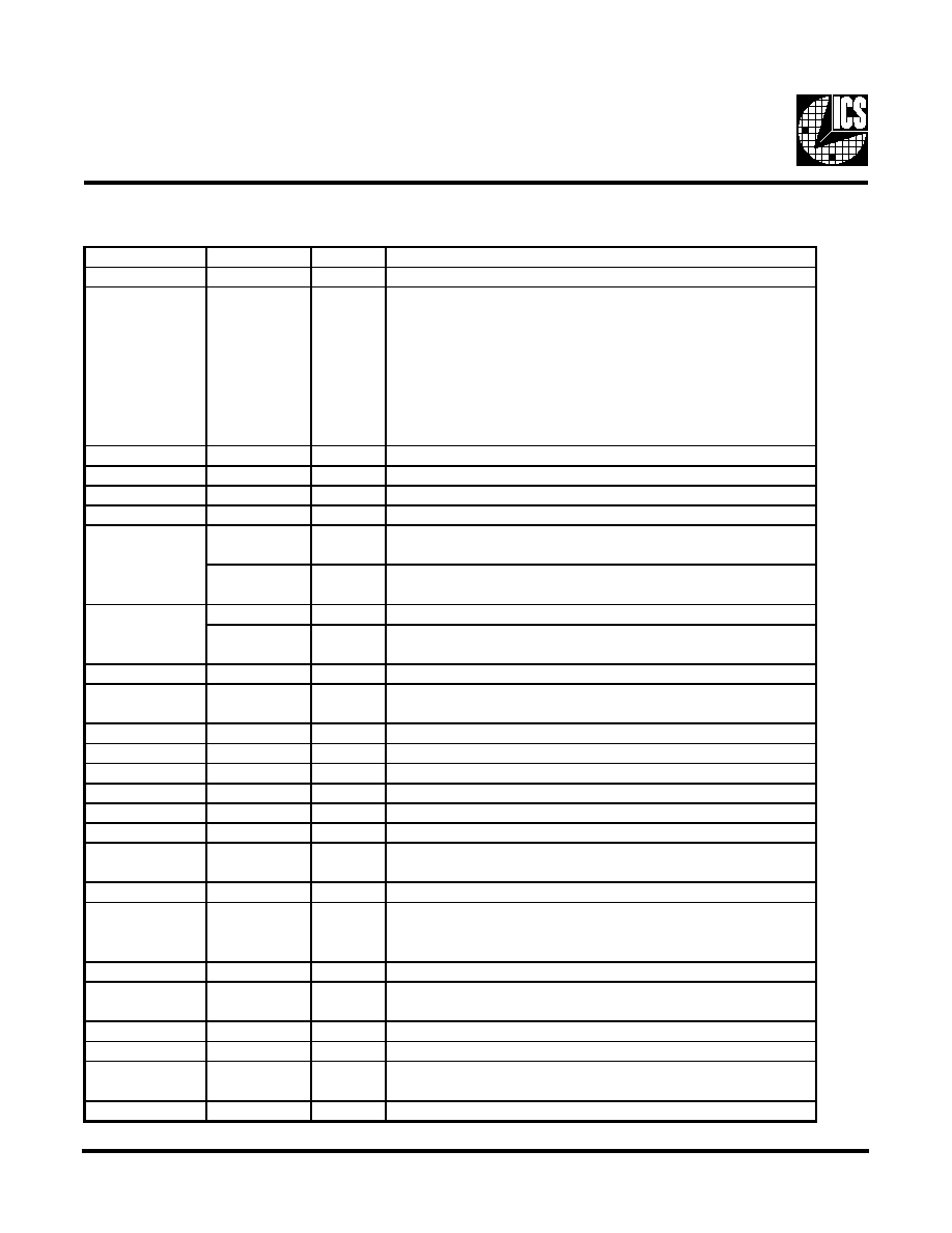
Block Diagram
Frequency Timing Generator for PENTIUM II/III Systems
9250-11 Rev C 3/20/00
Pin Configuration
56-pin SSOP
Generates the following system clocks:
- 6 - CPU Clocks 100/133MHz (2.5V).
- 2 - CPU/2 output for synchronous memory
reference (2.5V).
- 4 - fixed frequency Clocks @ 66.6MHz (3.3V).
- 2 - fixed frequency Clocks @ 33.3MHz (3.3V).
- 6 - IOAPIC Clocks @ º of CPUCLK or 16.667MHz,
synchronous to CPU Clock (2.5V)
- 1 - 48MHz Clock (3.3V)
- 2 - REF Clocks @ 14.31818MHz
0.5% typical down spread modulation on CPU, PCI,
IOAPIC, 3V66 and CPU/2 output clocks.
Uses external 14.318MHz crystal.
The ICS9250-11 is a main clock synthesizer chip for Pentium
II based systems using Rambus Interface DRAMs. This chip
provides all the clocks required for such a system when used
with a Direct Rambus Clock Generator (DRCG) chip such as
the ICS9212-01, 02, 03 and a PCI buffer 9112-17.
Spread Spectrum may be enabled by driving the SPREAD#
pin active. Spread spectrum typically reduces system EMI by
8dB to 10dB. This simplifies EMI qualification without
resorting to board design iterations or costly shielding. The
ICS9250-11 employs a proprietary closed loop design, which
tightly controls the percentage of spreading over process and
temperature variations.
The CPU/2 clocks are inputs to the DRCG.
SEL 133/100#
SEL(0:1)
SPREAD#
X1
X2
OSC
PLL
Spread
Spectrum
PLL2
CPU/2 (0:1)
REF (0:1)
2
6
4
2
2
CPUCLK (0:5)
3V66 (0:3)
48MHz
/ 2
/ 3
/ 2
3V33 (0:1)
C
o
n
t
r
o
l
/ 2
/ 2
/ 4
/ 3
/ 2
IOAPIC(0:5)
6
Power Groups:
VDDREF, GNDREF = REF, X1, X2
VDD66, GND66 = 3V66
VDD33, GND33 = 3V33
VDD48, GND48 = 48MHz
VDDCOR, GNDCOR = PLL Core
VDDLCPU, GNDLCPU = CPUCLK
VDDLCPU/2 , GNDLCPU/2 = CPU/2
VDDLAPIC, GNDAPIC = IOAPIC
ICS reserves the right to make changes in the device data identified in this
publication without further notice. ICS advises its customers to obtain the
latest version of all device data to verify that any information being relied
upon by the customer is current and accurate.
2
ICS9250-11
Pin Descriptions
Pin number
Pin name
Type
Description
1, 52, 53
GNDLAPIC
PWR
Ground pin for the IOAPIC outputs.
2, 3, 50, 51, 54, 55
IOAPIC (0:5)
OUT
2.5V clock outputs running divide synchronous with the CPU
(Host bus) clock frequency. The default APIC is running at º of
CPUCLK frequency.
When FREQ_APIC is strapped low, the APIC is running at fixed
16.67 MHz.
If CPU = 133 MHz, APIC = CPU/8
If CPU = 100 MHz, APIC = CPU/6
4, 49, 56
VDDLAPIC
PWR
Power pin for the IOAPIC outputs. 2.5V.
5, 11
VDDREF
PWR
Power pin for REF clocks
6
X1
IN
XTAL_IN 14.318MHz crystal input
7
X2
OUT
XTAL_OUT Crystal output
REF0
OUT
3.3V 14.318 MHz clock output. APIC clock strapping option for
fixed 16.67 MHz APIC clock outputs.
FREQ_APIC#
OUT
If FREQ_APIC# = 0, APIC Clock = 16.67 MHz
If FREQ_APIC# = Open, APIC Clock = CPU/4
REF1
OUT
3.3V 14.318MHz clock output.
TEST#
OUT
TEST# is sampled low (external with 10k pulldown). All clock
outputs are Tri-State.
12, 19
VDD66
PWR
power pin for the 3V66 clocks.
13, 14, 17, 18
3V66[0:3]
OUT
66MHz outputs at 3.3V. These outputs are stopped when
CPU_STOP# is driven active..
8, 15, 16, 23, 24
GND
PWR
Ground pin for 3V outputs.
21, 22
3V33MHz
OUT
3.3V Fixed 33MHz clock output.
25
VDDCOR
PWR
3.3V power for PLL core.
26
GND48
PWR
Ground pin for the 48MHz output
27
48MHz
OUT
Fixed 48MHz clock output. 3.3V
28
VDD48
PWR
Power pin for the 48MHz output.
29
SEL 133/100#
IN
This selects the frequency for the CPU and CPU/2 outputs. High =
133MHz, Low=100MHz
30, 31
SEL[0:1]
IN
Function select pins. See truth table for details.
32
SPREAD#
IN
Enables spread spectrum when active(Low). modulates all the CPU,
PCI, IOAPIC, 3V66 and CPU/2 clocks. Does not affect the REF and
48MHz clocks. 0.5% down spread modulation.
33
VDDLCPU/2
PWR
Power pin for the CPU/2 clocks. 2.5V
34, 35
CPU/2[0:1]
OUT
2.5V clock outputs at 1/2 CPU frequency. 66MHz or50MHz
depending on the state of the SEL 133/100# input pin.
36
GNDLCPU/2
PWR
Ground pin for the CPU/2 clocks.
37, 44, 45
GNDLCPU
PWR
Ground pin for the CPUCLKs
38, 39, 42, 43, 46,
47
CPUCLK[0:5]
OUT
Host bus clock output at 2.5V. 133MHz or 100MHz depending on
the state of the SEL 133/100MHz.
40, 41, 48
VDDLCPU
PWR
Power pin for the CPUCLKs. 2.5V
9
10
3
ICS9250-11
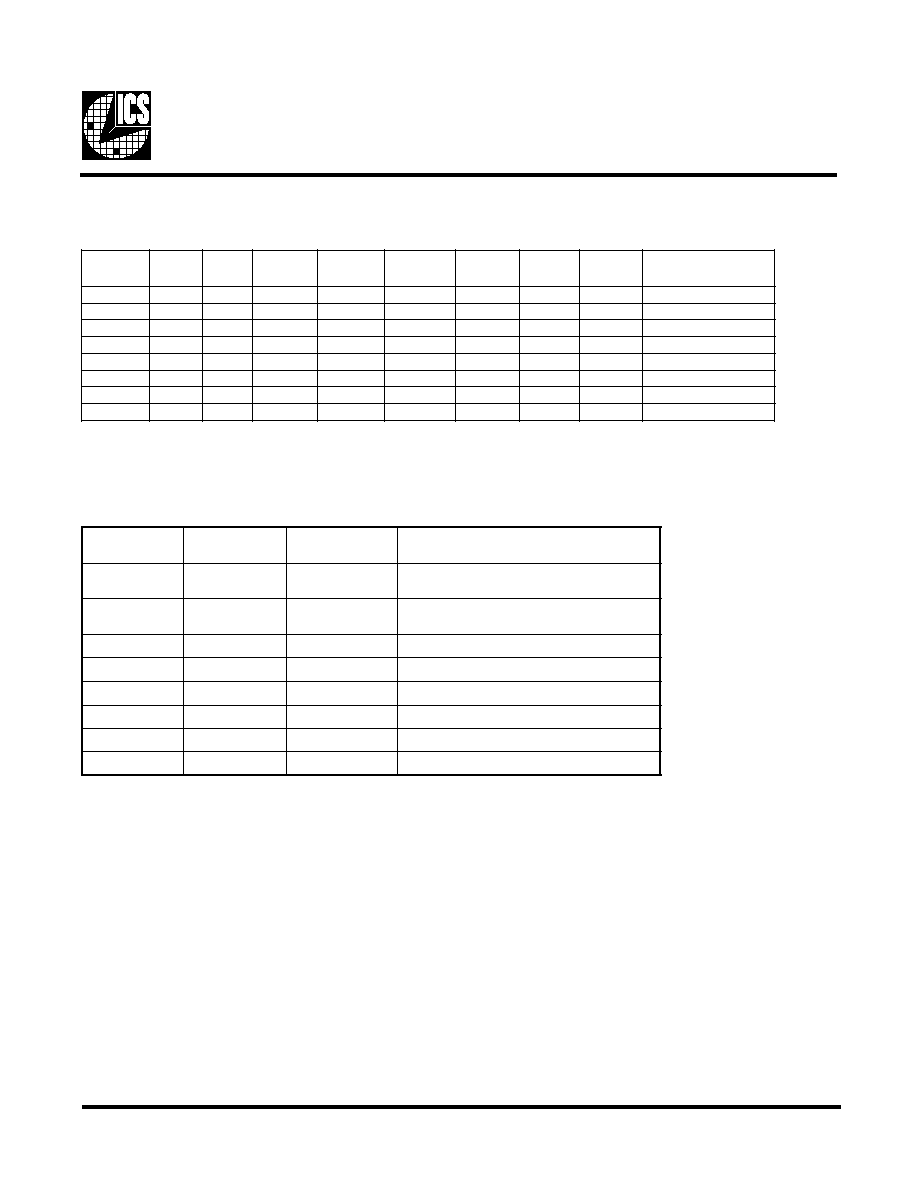
Frequency Select:
Power Management Features:
L
E
S
#
0
0
1
/
3
3
1
1
L
E
S
0
L
E
S
U
P
C
z
H
M
2
/
U
P
C
z
H
M
6
6
V
3
z
H
M
3
3
V
3
z
H
M
8
4
z
H
M
F
E
R
z
H
M
z
H
M
C
I
P
A
O
I
0
0
0
e
t
a
t
s
i
r
T
e
t
a
t
s
i
r
T
e
t
a
t
s
i
r
T
e
t
a
t
s
i
r
T
e
t
a
t
s
i
r
T
e
t
a
t
s
i
r
T
e
t
a
t
s
i
r
T
0
0
1
A
/
N
A
/
N
A
/
N
A
/
N
A
/
N
A
/
N
A
/
N
0
1
0
0
0
1
0
0
.
0
5
6
.
6
6
3
.
3
3
F
F
O
8
1
3
.
4
1
7
6
.
6
1
/
K
L
C
U
P
C
º
0
1
1
0
0
1
0
0
.
0
5
6
.
6
6
3
.
3
3
8
4
8
1
3
.
4
1
7
6
.
6
1
/
K
L
C
U
P
C
º
1
0
0
2
/
K
L
C
T
4
/
K
L
C
T
4
/
K
L
C
T
8
/
K
L
C
T
2
/
K
L
C
T
K
L
C
T
6
1
/
K
L
C
T
1
0
1
A
/
N
A
/
N
A
/
N
A
/
N
A
N
A
/
N
A
/
N
1
1
0
3
.
3
3
1
6
.
6
6
6
.
6
6
3
.
3
3
F
F
O
8
1
3
.
4
1
7
6
.
6
1
/
K
L
C
U
P
C
º
1
1
1
3
.
3
3
1
6
.
6
6
6
.
6
6
3
.
3
3
8
4
8
1
3
.
4
1
7
6
.
6
1
/
K
L
C
U
P
C
º
#
0
0
1
/
3
3
1
L
E
S
1
L
E
S
0
L
E
S
n
o
it
c
n
u
F
0
0
0
e
t
a
t
S
-i
r
T
st
u
p
t
u
o
ll
A
0
0
0
1
d
e
v
r
e
s
e
R
0
1
0
e
v
it
c
a
n
i
L
L
P
z
H
M
8
4
,z
H
M
0
0
1
e
v
it
c
A
0
1
1
e
v
it
c
a
L
L
P
z
H
M
8
4
,z
H
M
0
0
1
e
v
it
c
A
1
0
0
e
d
o
M
t
s
e
T
1
0
1
d
e
v
r
e
s
e
R
1
1
0
e
v
it
c
a
n
i
L
L
P
z
H
M
8
4
,z
H
M
3
3
1
e
v
it
c
A
1
1
1
e
v
it
c
a
L
L
P
z
H
M
8
4
,z
H
M
3
3
1
e
v
it
c
A

4
ICS9250-11
Absolute Maximum Ratings
Supply Voltage. . . . . . . . . . . . . . . . . . . . . . . . . . . 7.0 V
Logic Inputs . . . . . . . . . . . . . . . . . . . . . . . . . . . . . GND 0.5 V to V
DD
+0.5 V
Ambient Operating Temperature . . . . . . . . . . . . 0∞C to +70∞C
Storage Temperature . . . . . . . . . . . . . . . . . . . . . . 65∞C to +150∞C
Stresses above those listed under Absolute Maximum Ratings may cause permanent damage to the device. These ratings are stress
specifications only and functional operation of the device at these or any other conditions above those listed in the operational
sections of the specifications is not implied. Exposure to absolute maximum rating conditions for extended periods may affect
product reliability.
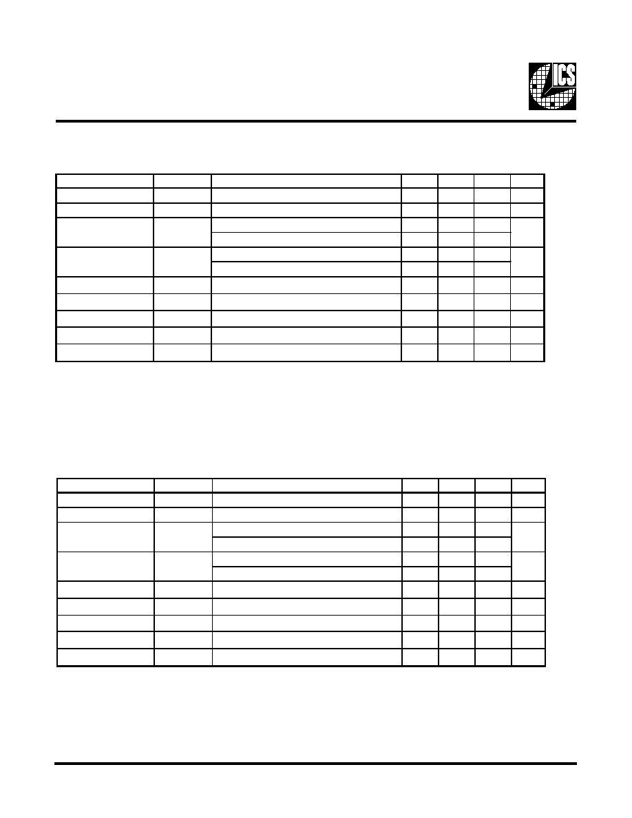
Electrical Characteristics - Input/Supply/Common Output Parameters
T
A
= 0 - 70C; Supply Voltage V
DD
= 3.3 V +/-5%, V
DDL
= 2.5 V +/-5% (unless otherwise stated)
PARAMETER
SYMBOL
CONDITIONS
MIN
TYP
MAX
UNITS
Input High Voltage
V
IH
2
V
DD
+0.3
V
Input Low Voltage
V
IL
V
SS
-0.3
0.8
V
Input High Current
I
IH
V
IN
= V
DD
5
µ
A
I
IL1
V
IN
= 0 V; Inputs with no pull-up resistors
-5
I
IL2
V
IN
= 0 V; Inputs with pull-up resistors
200
C
L
= Max loads; Select @ 100 MHz
160
C
L
= Max loads; Select @ 133 MHz
160
C
L
= Max loads; Select @ 100 MHz
75
C
L
= Max loads; Select @ 133 MHz
90
I
DD3.3P D
C
L
= Max loads
200
I
DD.25P D
Input address VDD or GND
100
Input Frequency
F
i
V
DD
= 3.3 V
14.318
MHz
Pin Inductance
1
L
pin
7
nH
C
IN
Logic Inputs
5
pF
C
OUT
Output pin capacitance
6
pF
C
INX
X1 & X2 pins
13.5
18
22.5
pF
Transition time
1
T
trans
To 1st crossing of target frequency
3
ms
Clk Stabilization
1
T
STAB
From V
DD
= 3.3 V to 1% target frequency
3
ms
t
P ZH
,t
P ZL
Output enable delay (all outputs)
1
8
ns
t
P HZ
,t
P LZ
Output disable delay (all outputs)
1
8
ns
T
CP U-3V66
CPU @ 1.25V, 3V66 @ 1.5V
0
1.5
ns
T
3V66-3V33
3V66 @ 1.5V, 3V33 @ 1.5V
1.5
3.5
ns
T
CP U-IOAP IC
CPU @ 1.25V, IOAPIC @ 1.25V
1.0
3.0
ns
1
Guaranteed by design, not 100% tested in production.
Input Low Current
µ
A
I
DD3.3OP
Delay
1
mA
Input Capacitance
1
I
DD.25OP
µ
A
Powerdown Current
Operating Supply
Current
mA
Skew
1

5
ICS9250-11
Electrical Characteristics - CPU
T
A
= 0 - 70C; V
DDL
= 2.5 V +/-5%; C
L
= 10-20 pF (unless otherwise specified)
PARAMETER
SYMBOL
CONDITIONS
MIN
TYP
MAX UNITS
Output High Voltage
V
OH2B
I
OH
= -12 mA
2
V
Output Low Voltage
V
OL2B
I
OL
= 12 mA
0.4
V
V
OH @ MIN
= 1.0 V
-27
V
OH @ MAX
= 2.375 V
-27
V
OL @ MIN
= 1.2 V
27
V
OL @ MAX
= 0.3 V
30
Rise Time
1
t
r2B
V
OL
= 0.4 V, V
OH
= 2.0 V
0.4
1.6
ns
Fall Time
1
t
f2B
V
OH
= 2.0 V, V
OL
= 0.4 V
0.4
1.6
ns
Duty Cycle
1
d
t2B
V
T
= 1.25 V
45
55
%
Skew window
1
t
sk2B
V
T
= 1.25 V
175
ps
Jitter, cycle-to-cycle
1
t
jcyc-cyc2B
V
T
= 1.25 V
150
ps
1
Guaranteed by design, not 100% tested in production.
mA
mA
Output High Current
Output Low Current
I
OH2B
I
OL2B
Electrical Characteristics - CPU/2
T
A
= 0 - 70C; V
DDL
= 2.5 V +/-5%; C
L
= 10-20 pF (unless otherwise specified)
PARAMETER
SYMBOL
CONDITIONS
MIN
TYP
MAX UNITS
Output High Voltage
V
OH2B
I
OH
= -12 mA
2
V
Output Low Voltage
V
OL2B
I
OL
= 12 mA
0.4
V
V
OH @ MIN
= 1.0 V
-27
V
OH @ MAX
= 2.375 V
-27
V
OL @ MIN
= 1.2 V
27
V
OL @ MAX
= 0.3 V
30
Rise Time
1
t
r2B
V
OL
= 0.4 V, V
OH
= 2.0 V
0.4
1.6
ns
Fall Time
1
t
f2B
V
OH
= 2.0 V, V
OL
= 0.4 V
0.4
1.6
ns
Duty Cycle
1
d
t2B
V
T
= 1.25 V
45
55
%
Skew window
1
t
sk2B
V
T
= 1.25 V
175
ps
Jitter, cycle-to-cycle
1
t
jcyc-cyc2B
V
T
= 1.25 V
250
ps
1
Guaranteed by design, not 100% tested in production.
mA
mA
Output High Current
Output Low Current
I
OH2B
I
OL2B
6
ICS9250-11
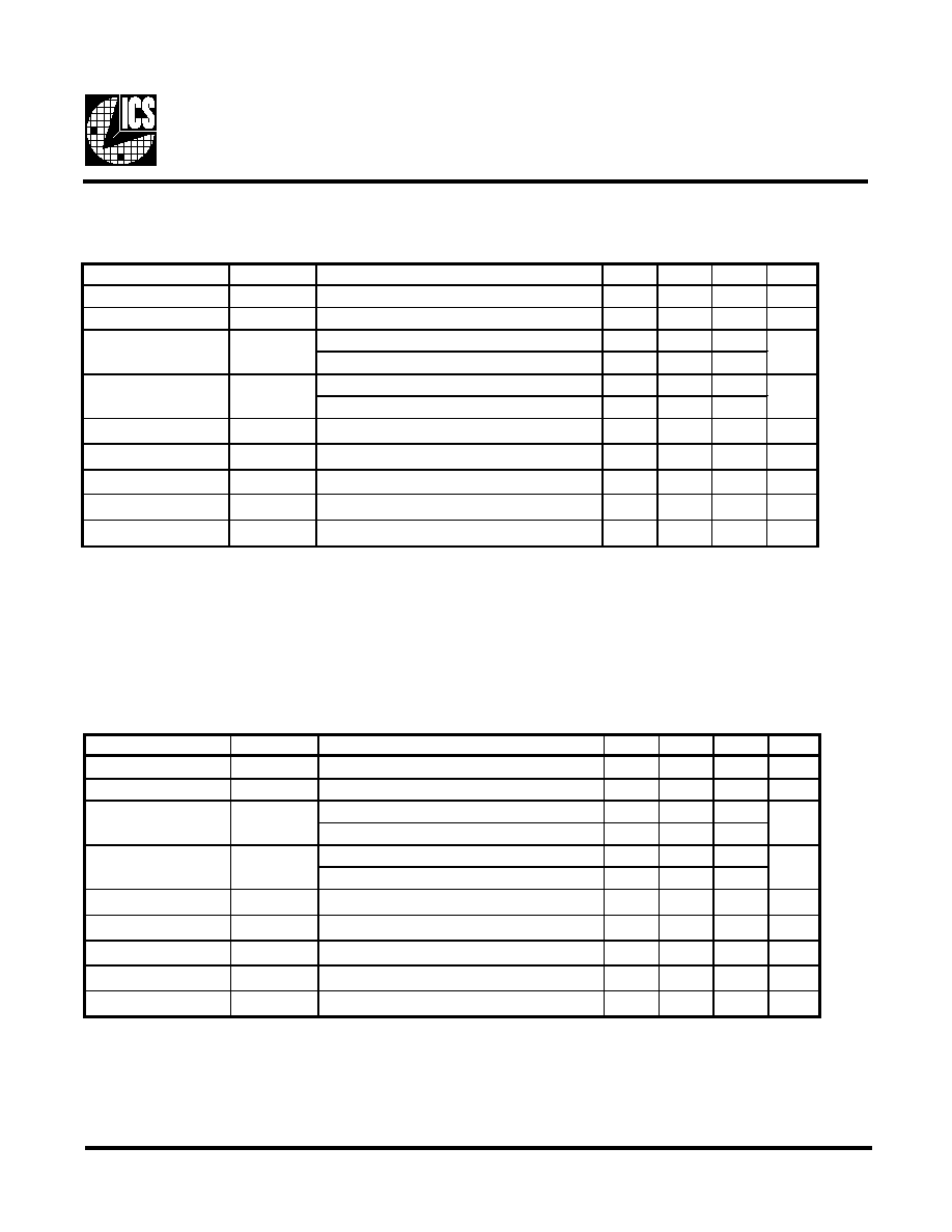
Electrical Characteristics - 3V33
T
A
= 0 - 70C; V
DD
= 3.3 V +/-5%; C
L
= 10-30 pF (unless otherwise specified)
PARAMETER
SYMBOL
CONDITIONS
MIN
TYP
MAX UNITS
Output High Voltage
V
OH1
I
OH
= -14.5 mA
2.4
V
Output Low Voltage
V
OL1
I
OL
= 9.4 mA
0.4
V
V
OH @ MIN
= 1.0 V
-33
V
OH @ MAX
= 3.135 V
-33
V
OL @ MIN
= 1.95 V
30
V
OL @ MAX
= 0.4 V
38
Rise Time
1
t
r1
V
OL
= 0.4 V, V
OH
= 2.4 V
0.5
2.0
ns
Fall Time
1
t
f1
V
OH
= 2.4 V, V
OL
= 0.4 V
0.5
2.0
ns
Duty Cycle
1
d
t1
V
T
= 1.5 V
45
55
%
Skew window
1
t
sk1
V
T
= 1.5 V
250
ps
Jitter, cycle-to-cycle
1
t
jcyc-cyc1
V
T
= 1.5 V
250
ps
1
Guaranteed by design, not 100% tested in production.
Output High Current
Output Low Current
mA
mA
I
OH1
I
OL1
Electrical Characteristics - 3V66
T
A
= 0 - 70C; V
DD
= 3.3 V +/-5%; C
L
= 10-30 pF (unless otherwise specified)
PARAMETER
SYMBOL
CONDITIONS
MIN
TYP
MAX UNITS
Output High Voltage
V
OH1
I
OH
= -14.5 mA
2.4
V
Output Low Voltage
V
OL1
I
OL
=9 mA
0.4
V
V
OH @ MIN
= 1.0 V
-33
V
OH @ MAX
= 3.135 V
-33
V
OL @ MIN
= 1.95 V
30
V
OL @ MAX
= 0.4 V
38
Rise Time
1
t
r1
V
OL
= 0.4 V, V
OH
= 2.4 V
0.5
2.0
ns
Fall Time
1
t
f1
V
OH
= 2.4 V, V
OL
= 0.4 V
0.5
2.0
ns
Duty Cycle
1
d
t1
V
T
= 1.5 V
45
55
%
Skew window
1
t
sk1
V
T
= 1.5 V
250
ps
Jitter, cycle-to-cycle
1
t
jcyc-cyc1
V
T
= 1.5 V
500
ps
1
Guaranteed by design, not 100% tested in production.
Output High Current
Output Low Current
mA
mA
I
OH1
I
OL1
7
ICS9250-11
Electrical Characteristics - REF, 48MHz
T
A
= 0 - 70C; V
DD
= 3.3 V +/-5%; C
L
= 10-20 pF (unless otherwise specified)
PARAMETER
SYMBOL
CONDITIONS
MIN
TYP
MAX UNITS
Output High Voltage
V
OH5
I
OH
= -16 mA
2.4
V
Output Low Voltage
V
OL5
I
OL
= 9 mA
0.4
V
V
OH @ MIN
= 1.0 V
-29
V
OH @ MAX
= 3.135 V
-23
V
OL @ MIN
= 1.95 V
29
V
OL @ MAX
= 0.4 V
27
Rise Time
1
t
r5
V
OL
= 0.4 V, V
OH
= 2.4 V
1.0
4.0
ns
Fall Time
1
t
f5
V
OH
= 2.4 V, V
OL
= 0.4 V
1.0
4.0
ns
Duty Cycle
1
d
t5
V
T
= 1.5 V
45
55
%
Jitter, cycle-to-cycle
1
t
jcyc-cyc5
V
T
= 1.5 V, Fixed clocks
500
ps
Jitter, cycle-to-cycle
1
t
jcyc-cyc5
V
T
= 1.5 V, Ref clocks
1000
ps
1
Guaranteed by design, not 100% tested in production.
Output High Current
I
OH5
mA
Output Low Current
I
OL5
mA
Electrical Characteristics - IOAPIC
T
A
= 0 - 70C; V
DDL
= 2.5 V +/-5%; C
L
= 10-20 pF (unless otherwise specified)
PARAMETER
SYMBOL
CONDITIONS
MIN
TYP
MAX UNITS
Output High Voltage
V
OH2B
I
OH
= -12 mA
2
V
Output Low Voltage
V
OL2B
I
OL
= 12 mA
0.4
V
V
OH @ MIN
= 1.0 V
-27
V
OH @ MAX
= 2.375 V
-27
V
OL @ MIN
= 1.2 V
27
V
OL @ MAX
= 0.3 V
30
Rise Time
1
t
r2B
V
OL
= 0.4 V, V
OH
= 2.0 V
0.4
1.6
ns
Fall Time
1
t
f2B
V
OH
= 2.0 V, V
OL
= 0.4 V
0.4
1.6
ns
Duty Cycle
1
d
t2B
V
T
= 1.25 V
45
55
%
Skew window
1
t
sk2B
V
T
= 1.25 V
250
ps
Jitter, cycle-to-cycle
1
t
jcyc-cyc2B
V
T
= 1.25 V
250
ps
1
Guaranteed by design, not 100% tested in production.
mA
mA
Output High Current
Output Low Current
I
OH2B
I
OL2B

8
ICS9250-11
ICS reserves the right to make changes in the device data identified in this
publication without further notice. ICS advises its customers to obtain the
latest version of all device data to verify that any information being relied
upon by the customer is current and accurate.
L
O
B
M
Y
S
S
N
O
I
S
N
E
M
I
D
N
O
M
M
O
C
S
N
O
I
T
A
I
R
A
V
D
N
.
N
I
M
.
M
O
N
.
X
A
M
.
N
I
M
.
M
O
N
.
X
A
M
A
5
9
0
.
2
0
1
.
0
1
1
.
D
A
0
2
7
.
5
2
7
.
0
3
7
.
6
5
1
A
8
0
0
.
2
1
0
.
6
1
0
.
2
A
7
8
0
.
0
9
0
.
4
9
0
.
B
8
0
0
.
-
5
3
1
0
.
c
5
0
0
.
-
0
1
0
.
D
s
n
o
i
t
a
i
r
a
V
e
e
S
E
1
9
2
.
5
9
2
.
9
9
2
.
e
C
S
B
5
2
0
.
0
H
5
9
3
.
-
0
2
4
.
h
0
1
0
.
3
1
0
.
6
1
0
.
L
0
2
0
.
-
0
4
0
.
N
s
n
o
i
t
a
i
r
a
V
e
e
S
µ
∞
0
-
∞
8
56 Pin 300 mil SSOP Package
"For current dimensional specifications, see JEDEC 95."
.093
DIA. PIN (Optional)
D/2
E/2
BOTTOM VIEW
A
2
SEE
DETAIL "A"
-E-
c
END VIEW
H
Pin 1
TOP VIEW
Index
Area
PARTING LINE
L
DETAIL "A"
A
1
-e-
B
A
SIDE VIEW
-C-
-D-
SEATING
PLANE
.004 C
Ordering Information
ICS9250yF-11-T
Designation for tape and reel packaging
Pattern Number (2 or 3 digit number for parts with ROM code patterns)
Package Type
F=SSOP
Revision Designator (will not correlate with datasheet revision)
Device Type (consists of 3 or 4 digit numbers)
Prefix
ICS, AV = Standard Device
Example:
ICS XXXX y F - PPP - T
Dimensions in inches