Äîêóìåíòàöèÿ è îïèñàíèÿ www.docs.chipfind.ru
Integrated
Circuit
Systems, Inc.
ICS9250-29
Third party brands and names are the property of their respective owners.
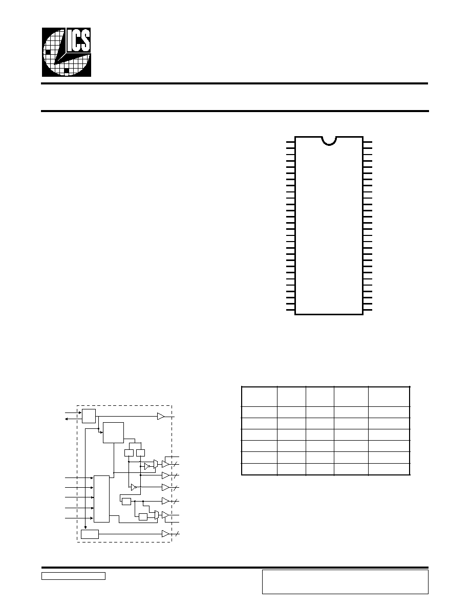
Block Diagram
9250-29 Rev A 02/01/01
Recommended Application:
Solano type chipset.
Output Features:
·
2 CPU (2.5V) (up to 133MHz achievable through I
2
C)
·
13 SDRAM (3.3V) (up to 133MHz achievable
through I
2
C)
·
5 PCI (3.3 V) @33.3MHz
·
1 IOAPIC (2.5V) @ 33.3 MHz
·
3 Hublink clocks (3.3 V) @ 66.6 MHz
·
2 (3.3V) @ 48 MHz (Non spread spectrum)
·
1 REF (3.3V) @ 14.318 MHz
Features:
·
Supports spread spectrum modulation,
0 to -0.5% down spread.
·
I
2
C support for power management
·
Efficient power management scheme through PD#
·
Uses external 14.138 MHz crystal
·
Alternate frequency selections available through I
2
C
control.
Functionality
Pin Configuration
56-Pin 300mil SSOP
* This input has a 50K
9 pull-down to GND.
** This input has a 50K
9pull-up to VDD
IOAPIC
VDDL
GNDL
*FS1/REF
VDDR
X1
X2
GNDR
VDD3
3V66-0
3V66-1
3V66-2
GND3
PCICLK0
PCICLK1
PCICLK2
VDD2
GND2
PCICLK3
PCICLK4
FS0
GNDA
VDDA
SCLK
SDATA
GNDF
VDDF
48MHz_0
GNDL
VDDL
CPUCLK0
CPUCLK1
GND1
SDRAM0
SDRAM1
VDD1
GND1
SDRAM2
SDRAM3
SDRAM4
SDRAM5
VDD1
GND1
SDRAM6
SDRAM7
SDRAM8
SDRAM9
VDD1
GND1
SDRAM10
SDRAM11
VDD1
GND1
SDRAM12
TRISTATE#/PD#**
48MHz_1
ICS9250-29
1
2
3
4
5
6
7
8
9
10
11
12
13
14
15
16
17
18
19
20
21
22
23
24
25
26
27
28
56
55
54
53
52
51
50
49
48
47
46
45
44
43
42
41
40
39
38
37
36
35
34
33
32
31
30
29
Frequency Generator & Integrated Buffers for Celeron & PII/IIITM
REF
CPU66/100/133 [1:0]
VDDL
3V66 [2:0]
SDRAM [12:0]
PCICLK [4:0]
IOAPIC
VDDL
PLL2
48MHz [1:0]
X1
X2
XTAL
OSC
Control
Logic
Config
Reg
FS(1:0)
PD#
TRISTATE#
2
2
3
13
5
/2
/2
/3
/2
PLL1
Spread
Spectrum
SDATA
SCLK
#
e
t
a
t
s
i
r
T
0
S
F
1
S
F
U
P
C
z
H
M
M
A
R
D
S
z
H
M
0
0
X
e
t
a
t
s
i
r
T
e
t
a
t
s
i
r
T
0
1
X
t
s
e
T
t
s
e
T
1
0
0
z
H
M
6
6
z
H
M
0
0
1
1
1
0
z
H
M
0
0
1
z
H
M
0
0
1
1
0
1
z
H
M
3
3
1
z
H
M
3
3
1
1
1
1
z
H
M
3
3
1
z
H
M
0
0
1
ICS reserves the right to make changes in the device data identified in this
publication without further notice. ICS advises its customers to obtain the
latest version of all device data to verify that any information being relied
upon by the customer is current and accurate.
Power Groups
VDDA, GNDA = CPU, PLL (analog)
VDDF, GNDF = Fixed PLL, 48M (analog/digital)
VDDR, GNDR = REF, X1, X2 (analog/digital)
VDD3, GND3 = 3V66 (digital)
VDD2, GND2 = PCI (digital)
VDD1, GND1 = SDRAM (digital)
VDDL, GNDL = IOAPIC, CPU (digital)

2
ICS9250-29
The ICS9250-29 is a single chip clock solution for Solano type chipset. It provides all necessary clock signals for such
a system.
Spread spectrum may be enabled through I
2
C programming. Spread spectrum typically reduces EMI by 8dB to 10 dB.
This simplifies EMI qualification without resorting to board design iterations or costly shielding. The ICS9250-29
employs a proprietary closed loop design, which tightly controls the percentage of spreading over process and
temperature variations.
General Description
Pin Configuration
R
E
B
M
U
N
N
I
P
E
M
A
N
N
I
P
E
P
Y
T
N
O
I
T
P
I
R
C
S
E
D
1
C
I
P
A
O
I
T
U
O
.
z
H
M
3
.
3
3
t
a
g
n
i
n
n
u
r
t
u
p
t
u
o
k
c
o
l
c
V
5
.
2
5
5
,
2
L
D
D
V
R
W
P
C
I
P
A
O
I
&
U
P
C
r
o
f
y
l
p
p
u
s
r
e
w
o
p
V
5
.
2
6
5
,
3
L
D
N
G
R
W
P
C
I
P
A
O
I
&
U
P
C
r
o
f
y
l
p
p
u
s
r
e
w
o
p
V
5
.
2
r
o
f
d
n
u
o
r
G
4
1
S
F
N
I
y
t
i
l
a
n
o
i
t
c
n
u
f
t
u
p
t
u
o
l
l
a
,
y
c
n
e
u
q
e
r
f
U
P
C
s
e
n
i
m
r
e
t
e
D
.
n
i
p
t
c
e
l
e
S
n
o
i
t
c
n
u
F
F
E
R
T
U
O
.
t
u
p
t
u
o
k
c
o
l
c
e
c
n
e
r
e
f
e
r
z
H
M
8
1
3
.
4
1
,
V
3
.
3
,
7
2
,
3
2
,
7
1
,
9
,
5
9
4
,
3
4
,
7
3
,
3
3
x
D
D
V
R
W
P
y
l
p
p
u
s
r
e
w
o
p
V
3
.
3
6
1
X
N
I
k
c
a
b
d
e
e
f
d
n
a
)
F
p
3
3
(
p
a
c
d
a
o
l
l
a
n
r
e
t
n
i
s
a
h
,
t
u
p
n
i
l
a
t
s
y
r
C
2
X
m
o
r
f
r
o
t
s
i
s
e
r
7
2
X
T
U
O
d
a
o
l
l
a
n
r
e
t
n
i
s
a
H
.
z
H
M
8
1
3
.
4
1
y
l
l
a
n
i
m
o
n
,
t
u
p
t
u
o
l
a
t
s
y
r
C
)
F
p
3
3
(
p
a
c
,
6
2
,
2
2
,
8
1
,
3
1
,
8
2
5
,
8
4
,
2
4
,
6
3
,
2
3
x
D
N
G
R
W
P
y
l
p
p
u
s
V
3
.
3
r
o
f
s
n
i
p
d
n
u
o
r
G
0
1
,
1
1
,
2
1
)
0
:
2
(
6
6
V
3
T
U
O
B
U
H
r
o
f
s
t
u
p
t
u
o
k
c
o
l
c
z
H
M
6
6
d
e
x
i
F
V
3
.
3
1
2
0
S
F
N
I
.
y
t
i
l
a
n
o
i
t
c
n
u
f
t
u
p
t
u
o
l
l
a
,
y
c
n
e
u
q
e
r
f
U
P
C
s
e
n
i
m
r
e
t
e
D
.
n
i
p
t
c
e
l
e
S
n
o
i
t
c
n
u
F
4
1
,
5
1
,
6
1
,
9
1
,
0
2
)
0
:
4
(
K
L
C
I
C
P
T
U
O
s
t
u
p
t
u
o
k
c
o
l
c
I
C
P
V
3
.
3
0
3
#
E
T
A
T
S
I
R
T
N
I
#
E
T
A
T
S
I
R
T
e
h
t
o
t
s
t
l
u
a
f
e
d
n
i
p
#
D
P
/
#
E
T
A
T
S
I
R
T
e
h
t
p
u
r
e
w
o
p
t
A
d
e
r
a
h
S
e
e
s
(
.
s
e
d
o
m
T
S
E
T
d
n
a
#
E
T
A
T
S
I
R
T
e
h
t
e
l
b
a
n
e
o
t
n
o
i
t
c
n
u
f
t
u
p
n
i
.
)
n
o
i
t
p
i
r
c
s
e
d
l
l
u
f
r
o
f
n
o
i
t
a
r
e
p
O
n
i
P
#
D
P
N
I
o
t
n
i
e
c
i
v
e
d
e
h
t
n
w
o
d
r
e
w
o
p
o
t
d
e
s
u
n
i
p
t
u
p
n
i
w
o
l
e
v
i
t
c
a
s
u
o
n
o
r
h
c
n
y
s
A
d
n
a
O
C
V
e
h
t
d
n
a
d
e
l
b
a
s
i
d
e
r
a
s
k
c
o
l
c
l
a
n
r
e
t
n
i
e
h
T
.
e
t
a
t
s
r
e
w
o
p
w
o
l
a
e
b
t
o
n
l
l
i
w
n
w
o
d
r
e
w
o
p
e
h
t
f
o
y
c
n
e
t
a
l
e
h
T
.
d
e
p
p
o
t
s
e
r
a
l
a
t
s
y
r
c
e
h
t
.
s
m
3
n
a
h
t
r
e
t
a
e
r
g
4
2
K
L
C
S
N
I
I
f
o
t
u
p
n
i
k
c
o
l
C
2
t
u
p
n
i
C
5
2
A
T
A
D
S
N
I
I
r
o
f
t
u
p
n
i
a
t
a
D
2
.
t
u
p
n
i
l
a
i
r
e
s
C
8
2
,
9
2
)
0
:
1
(
z
H
M
8
4
T
U
O
.
s
t
u
p
t
u
o
k
c
o
l
c
z
H
M
8
4
d
e
x
i
F
V
3
.
3
,
8
3
,
5
3
,
4
3
,
1
3
,
4
4
,
1
4
,
0
4
,
9
3
1
5
,
0
5
,
7
4
,
6
4
,
5
4
M
A
R
D
S
]
0
:
2
1
[
T
U
O
n
a
c
s
t
u
p
t
u
o
M
A
R
D
S
l
l
A
.
z
H
M
3
3
1
d
n
a
z
H
M
0
0
1
g
n
i
n
n
u
r
t
u
p
t
u
o
V
3
.
3
I
h
g
u
o
r
h
t
f
f
o
d
e
n
r
u
t
e
b
2
C
4
5
,
3
5
)
0
:
1
(
K
L
C
U
P
C
T
U
O
g
n
i
d
n
e
p
e
d
z
H
M
3
3
1
r
o
z
H
M
0
0
1
,
z
H
M
6
6
.
t
u
p
t
u
o
k
c
o
l
c
s
u
b
t
s
o
H
V
5
.
2
.
s
n
i
p
S
F
n
o
3
ICS9250-29
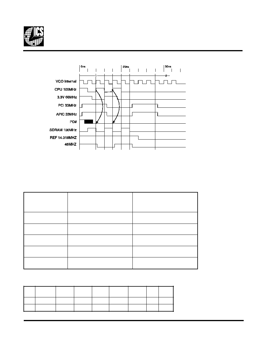
Power Down Waveform
Note
1. After PD# is sampled active (Low) for 2 consective rising edges of CPUCLKs, all the
output clocks are driven Low on their next High to Low tranistiion.
2. Power-up latency <3ms.
3. Waveform shown for 100MHz
Maximum Allowed Current
Clock Enable Configuration
#
D
P
K
L
C
U
P
C
M
A
R
D
S
C
I
P
A
O
I
6
6
V
3
K
L
C
I
C
P
,
F
E
R
z
H
M
8
4
c
s
O
s
O
C
V
0
W
O
L
W
O
L
W
O
L
W
O
L
W
O
L
W
O
L
F
F
O
F
F
O
1
N
O
N
O
N
O
N
O
N
O
N
O
N
O
N
O
o
n
a
l
o
S
n
o
i
t
i
d
n
o
C
n
o
i
t
p
m
u
s
n
o
c
y
l
p
p
u
s
V
5
.
2
x
a
M
,
s
d
a
o
l
p
a
c
e
t
e
r
c
s
i
d
x
a
M
V
5
2
6
.
2
=
2
q
d
d
V
D
N
G
r
o
3
q
d
d
V
=
s
t
u
p
n
i
c
i
t
a
t
s
l
l
A
n
o
i
t
p
m
u
s
n
o
c
y
l
p
p
u
s
V
3
.
3
x
a
M
,
s
d
a
o
l
p
a
c
e
t
e
r
c
s
i
d
x
a
M
V
5
6
4
.
3
=
3
q
d
d
V
D
N
G
r
o
3
q
d
d
V
=
s
t
u
p
n
i
c
i
t
a
t
s
l
l
A
e
d
o
M
n
w
o
d
r
e
w
o
P
)
0
=
#
N
W
D
R
W
P
(
A
m
2
A
m
2
z
H
M
6
6
e
v
i
t
c
A
l
l
u
F
0
0
=
)
0
:
1
(
S
F
A
m
5
3
A
m
0
4
4
z
H
M
0
0
1
e
v
i
t
c
A
l
l
u
F
1
0
=
)
0
:
1
(
S
F
A
m
0
5
A
m
0
3
4
z
H
M
3
3
1
e
v
i
t
c
A
l
l
u
F
1
1
=
)
0
:
1
(
S
F
A
m
0
6
A
m
0
4
4
z
H
M
3
3
1
e
v
i
t
c
A
l
l
u
F
0
1
=
)
0
:
1
(
S
F
A
m
0
6
A
m
0
0
5
4
ICS9250-29
1.
The ICS clock generator is a slave/receiver, I
2
C (SMB) component. It is only a "write" mode SMB device, no readback on
this part. Read-Back will lock up the PIIX-4 due to the Byte count of 00
H
.
2.
The data transfer rate supported by this clock generator is 100K bits/sec or less (standard mode)
3.
The input is operating at 3.3V logic levels.
4.
The data byte format is 8 bit bytes.
5.
To simplify the clock generator I
2
C interface, the protocol is set to use only "Block-Writes" from the controller. The bytes
must be accessed in sequential order from lowest to highest byte with the ability to stop after any complete byte has been
transferred. The Command code and Byte count shown above must be sent, but the data is ignored for those two bytes. The
data is loaded until a Stop sequence is issued.
6.
At power-on, all registers are set to a default condition, as shown.
General I
2
C serial interface information
The information in this section assumes familiarity with I
2
C programming.
For more information, contact ICS for an I
2
C programming application note.
How to Write:
· Controller (host) sends a start bit.
· Controller (host) sends the write address D2
(H)
· ICS clock will acknowledge
· Controller (host) sends a dummy command code
· ICS clock will acknowledge
· Controller (host) sends a dummy byte count
· ICS clock will acknowledge
· Controller (host) starts sending first byte (Byte 0) through byte 5
· ICS clock will acknowledge each byte one at a time.
· Controller (host) sends a Stop bit
Notes:
Controller (Host)
ICS (Slave/Receiver)
Start Bit
Address
D2
(H)
ACK
Dummy Command Code
ACK
Dummy Byte Count
ACK
Byte 0
ACK
Byte 1
ACK
Byte 2
ACK
Byte 3
ACK
Byte 4
ACK
Byte 5
ACK
Stop Bit
How to Write:
Note: This clock does not support Read Back. Doing a
read back will lock up the PIIX-4 system.
5
ICS9250-29
e
t
a
t
s
i
r
T
0
S
F
1
S
F
U
P
C
M
A
R
D
S
6
6
V
3
I
C
P
z
H
M
8
4
F
E
R
C
I
P
A
O
I
0
0
X
e
t
a
t
s
i
r
T
e
t
a
t
s
i
r
T
e
t
a
t
s
i
r
T
e
t
a
t
s
i
r
T
e
t
a
t
s
i
r
T
e
t
a
t
s
i
r
T
e
t
a
t
s
i
r
T
0
1
X
2
/
K
L
C
T
2
/
K
L
C
T
3
/
K
L
C
T
6
/
K
L
C
T
2
/
K
L
C
T
K
L
C
T
6
/
K
L
C
T
1
0
0
z
H
M
6
.
6
6
z
H
M
0
0
1
z
H
M
6
.
6
6
z
H
M
3
.
3
3
z
H
M
8
4
z
H
M
8
1
3
.
4
1
z
H
M
3
.
3
3
1
1
0
z
H
M
0
0
1
z
H
M
0
0
1
z
H
M
6
.
6
6
z
H
M
3
.
3
3
z
H
M
8
4
z
H
M
8
1
3
.
4
1
z
H
M
3
.
3
3
1
0
1
z
H
M
3
3
1
z
H
M
3
3
1
z
H
M
6
.
6
6
z
H
M
3
.
3
3
z
H
M
8
4
z
H
M
8
1
3
.
4
1
z
H
M
3
.
3
3
1
1
1
z
H
M
3
3
1
z
H
M
0
0
1
z
H
M
6
.
6
6
z
H
M
3
.
3
3
z
H
M
8
4
z
H
M
8
1
3
.
4
1
z
H
M
3
.
3
3
Truth Table
Byte 0: Control Register
(1 = enable, 0 = disable)
Byte 1: Control Register
(1 = enable, 0 = disable)
t
i
B
#
n
i
P
e
m
a
N
D
W
P
n
o
i
t
p
i
r
c
s
e
D
7
t
i
B
-
)
D
I
d
e
v
r
e
s
e
R
(
0
)
e
v
i
t
c
a
n
I
/
e
v
i
t
c
A
(
6
t
i
B
-
)
D
I
d
e
v
r
e
s
e
R
(
0
)
e
v
i
t
c
a
n
I
/
e
v
i
t
c
A
(
5
t
i
B
-
)
D
I
d
e
v
r
e
s
e
R
(
0
)
e
v
i
t
c
a
n
I
/
e
v
i
t
c
A
(
4
t
i
B
-
)
D
I
d
e
v
r
e
s
e
R
(
1
)
e
v
i
t
c
a
n
I
/
e
v
i
t
c
A
(
3
t
i
B
-
m
u
r
t
c
e
p
S
d
a
e
r
p
S
0
)
f
f
O
=
0
/
n
O
=
1
(
2
t
i
B
9
2
1
_
z
H
M
8
4
1
)
e
v
i
t
c
a
n
I
/
e
v
i
t
c
A
(
1
t
i
B
8
2
0
_
z
H
M
8
4
1
)
e
v
i
t
c
a
n
I
/
e
v
i
t
c
A
(
0
t
i
B
-
)
D
I
d
e
v
r
e
s
e
R
(
0
)
e
v
i
t
c
a
n
I
/
e
v
i
t
c
A
(
t
i
B
#
n
i
P
e
m
a
N
D
W
P
n
o
i
t
p
i
r
c
s
e
D
7
t
i
B
0
4
7
M
A
R
D
S
1
)
e
v
i
t
c
a
n
I
/
e
v
i
t
c
A
(
6
t
i
B
1
4
6
M
A
R
D
S
1
)
e
v
i
t
c
a
n
I
/
e
v
i
t
c
A
(
5
t
i
B
4
4
5
M
A
R
D
S
1
)
e
v
i
t
c
a
n
I
/
e
v
i
t
c
A
(
4
t
i
B
5
4
4
M
A
R
D
S
1
)
e
v
i
t
c
a
n
I
/
e
v
i
t
c
A
(
3
t
i
B
6
4
3
M
A
R
D
S
1
)
e
v
i
t
c
a
n
I
/
e
v
i
t
c
A
(
2
t
i
B
7
4
2
M
A
R
D
S
1
)
e
v
i
t
c
a
n
I
/
e
v
i
t
c
A
(
1
t
i
B
0
5
1
M
A
R
D
S
1
)
e
v
i
t
c
a
n
I
/
e
v
i
t
c
A
(
0
t
i
B
1
5
0
M
A
R
D
S
1
)
e
v
i
t
c
a
n
I
/
e
v
i
t
c
A
(
Note:
Reserved ID bits must be written with "0"