
Integrated
Circuit
Systems, Inc.
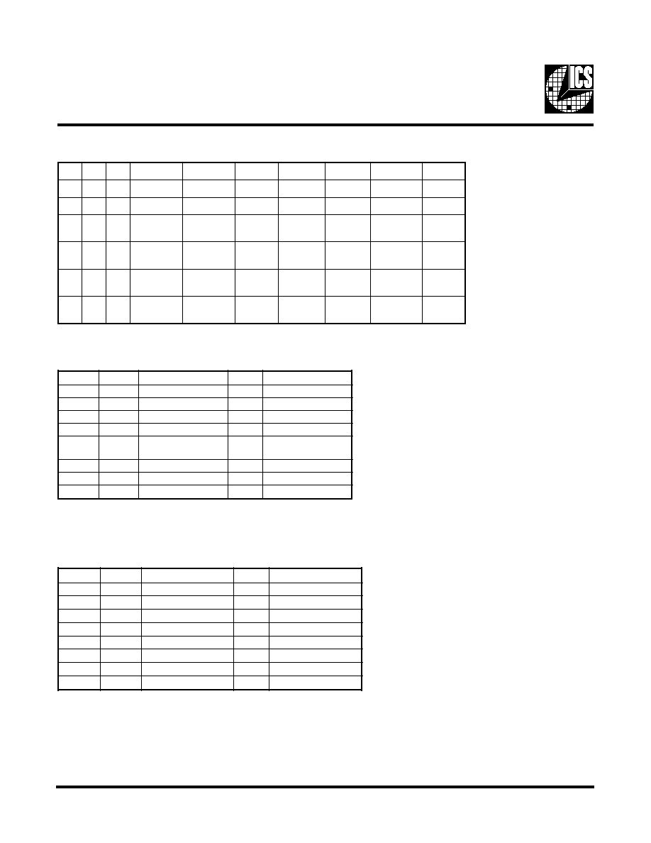
ICS9250-51
Block Diagram
0405A--03/22/02
Recommended Application:
815 B-Step type chipset.
Output Features:
∑
3 CPU (2.5V) (up to 133MHz achievable through
I
2
C)
∑
9 SDRAM (3.3V) (up to 133MHz achievable
through I
2
C)
∑
7 PCI (3.3 V) @33.3MHz
∑
2 IOAPIC (2.5V) @ 33.3 MHz
∑
3 Hublink clocks (3.3 V) @ 66.6 MHz
∑
2 (3.3V) @ 48 MHz (Non spread spectrum)
∑
1 REF (3.3V) @ 14.318 MHz
Features:
∑
Supports spread spectrum modulation,
0 to -0.5% down spread.
∑
I
2
C support for power management
∑
Efficient power management scheme through PD#
∑
Uses external 14.138 MHz crystal
∑
Alternate frequency selections available through I
2
C
control.
∑
815 B-Step compliant for frequency select latched
inputs. Internal power-on-reset and latching, are
delayed until Vtt_PWRGD signal is gated high onto
the PD#.
Functionality
Pin Configuration
56-Pin 300mil SSOP
* This input has a 50K
pull-down to GND.
*FS2//REF0
VDD
X1
X2
GND
GND
3V66-0
3V66-1
3V66-2
VDD
VDD
PCICLK_F
PCICLK0
GND
PCICLK1
PCICLK2
GND
PCICLK3
PCICLK4
PCICLK5
VDD
AVDD
AGND
GND
48MHz_0
48MHz_1
VDD48
FS0
GNDL
IOAPIC0
IOAPIC1
VDDL
CPUCLK0
VDDL0
CPUCLK1
CPUCLK2
GNDL
GND
SDRAM0
SDRAM1
VDD
SDRAM2
SDRAM3
GND
SDRAM4
SDRAM5
VDD
SDRAM6
SDRAM7
GND
SDRAM_F
VDD
Vtt_PWRGD/PD#
SCLK
SDATA
FS1
ICS9250-51
1
2
3
4
5
6
7
8
9
10
11
12
13
14
15
16
17
18
19
20
21
22
23
24
25
26
27
28
56
55
54
53
52
51
50
49
48
47
46
45
44
43
42
41
40
39
38
37
36
35
34
33
32
31
30
29
Frequency Generator & Integrated Buffers for Celeron & P
II
/
III
TM
2
S
F
1
S
F
0
S
F
n
o
i
t
c
n
u
F
X
0
0
e
t
a
t
s
i
r
T
X
0
1
t
s
e
T
0
1
0
z
H
M
6
6
=
U
P
C
e
v
it
c
A
z
H
M
0
0
1
=
M
A
R
D
S
0
1
1
z
H
M
0
0
1
=
U
P
C
e
v
it
c
A
z
H
M
0
0
1
=
M
A
R
D
S
1
1
0
z
H
M
3
3
1
=
U
P
C
e
v
it
c
A
z
H
M
3
3
1
=
M
A
R
D
S
1
1
1
z
H
M
3
3
1
=
U
P
C
e
v
it
c
A
z
H
M
0
0
1
=
M
A
R
D
S
REF0
CPU66/100/133 (2:0)
VDDL
3V66 (2:0)
SDRAM (7:0)
PCICLK (5:0)
IOAPIC (1:0)
VDDL
SDRAM_F
PCICLK_F
PLL2
48MHz (1:0)
X1
X2
XTAL
OSC
Control
Logic
Config
Reg
FS (2:0)
PD#
Vtt_PWRGD
2
3
3
8
6
2
/2
/2
/3
/2
PLL1
Spread
Spectrum
SDATA
SCLK
Power Groups
AVDD = Pin 22 Analog power for PLL
AGND = Pin 23 Analog ground
VDD48 = Pin 27 Analog power for 48MHz PLL
GND48 = Pin 24 Analog ground for 48MHz PLL

2
ICS9250-51
The ICS9250-51 is a single chip clock solution for 815 B-Step type chipset. It provides all necessary clock
signals for such a system.
Spread spectrum may be enabled through I
2
C programming. Spread spectrum typically reduces EMI by 8dB
to 10 dB. This simplifies EMI qualification without resorting to board design iterations or costly shielding. The
ICS9250-51 employs a proprietary closed loop design, which tightly controls the percentage of spreading over
process and temperature variations.
General Description
Pin Configuration
R
E
B
M
U
N
N
I
P
E
M
A
N
N
I
P
E
P
Y
T
N
O
I
T
P
I
R
C
S
E
D
1
2
S
F
N
I
y
t
il
a
n
o
i
t
c
n
u
f
t
u
p
t
u
o
ll
a
,
y
c
n
e
u
q
e
r
f
U
P
C
s
e
n
i
m
r
e
t
e
D
.
n
i
p
t
c
e
l
e
S
n
o
i
t
c
n
u
F
0
F
E
R
T
U
O
.
t
u
p
t
u
o
k
c
o
l
c
e
c
n
e
r
e
f
e
r
z
H
M
8
1
3
.
4
1
,
V
3
.
3
3
1
X
N
I
k
c
a
b
d
e
e
f
d
n
a
)
F
p
3
3
(
p
a
c
d
a
o
l
l
a
n
r
e
t
n
i
s
a
h
,
t
u
p
n
i
l
a
t
s
y
r
C
2
X
m
o
r
f
r
o
t
s
i
s
e
r
4
2
X
T
U
O
d
a
o
l
l
a
n
r
e
t
n
i
s
a
H
.
z
H
M
8
1
3
.
4
1
y
l
l
a
n
i
m
o
n
,
t
u
p
t
u
o
l
a
t
s
y
r
C
)
F
p
3
3
(
p
a
c
,
4
2
,
7
1
,
4
1
,
6
,
5
6
5
,
8
4
,
7
4
,
1
4
,
5
3
D
N
G
R
W
P
y
l
p
p
u
s
V
3
.
3
r
o
f
s
n
i
p
d
n
u
o
r
G
7
,
8
,
9
)
0
:
2
(
6
6
V
3
T
U
O
B
U
H
r
o
f
s
t
u
p
t
u
o
k
c
o
l
c
z
H
M
6
6
d
e
x
i
F
V
3
.
3
,
1
2
,
1
1
,
0
1
,
2
4
4
,
8
3
,
3
3
D
D
V
R
W
P
y
l
p
p
u
s
r
e
w
o
p
V
3
.
3
2
1
F
_
K
L
C
I
C
P
T
U
O
t
u
p
t
u
o
k
c
o
l
c
I
C
P
V
3
.
3
g
n
i
n
n
u
r
e
e
r
F
,
6
1
,
8
1
,
9
1
,
0
2
3
1
,
5
1
)
0
:
5
(
K
L
C
I
C
P
T
U
O
s
t
u
p
t
u
o
k
c
o
l
c
I
C
P
V
3
.
3
5
2
0
_
z
H
M
8
4
T
U
O
B
S
U
r
o
f
s
t
u
p
t
u
o
k
c
o
l
c
z
H
M
8
4
d
e
x
i
F
V
3
.
3
6
2
1
_
z
H
M
8
4
T
U
O
e
c
a
f
r
e
t
n
i
o
e
d
i
v
/
s
c
i
h
p
a
r
g
r
o
f
t
u
p
t
u
o
r
e
g
n
o
r
t
S
.
t
u
p
t
u
o
k
c
o
l
c
z
H
M
8
4
d
e
x
i
f
V
3
.
3
)
e
t
a
r
e
g
d
e
s
n
/
V
1
m
u
m
i
n
i
m
(
2
2
D
D
V
A
R
W
P
L
L
P
U
P
C
V
3
.
3
r
o
f
y
l
p
p
u
s
r
e
w
o
p
g
o
l
a
n
A
3
2
D
N
G
A
R
W
P
L
L
P
U
P
C
r
o
f
d
n
u
o
r
g
g
o
l
a
n
A
7
2
8
4
D
D
V
R
W
P
L
L
P
z
H
M
8
4
r
o
f
r
e
w
o
p
g
o
l
a
n
A
8
2
,
9
2
)
0
:
1
(
S
F
N
I
e
s
a
e
l
P
.
y
t
il
a
n
o
i
t
c
n
u
f
t
u
p
t
u
o
ll
a
,
y
c
n
e
u
q
e
r
f
U
P
C
s
e
n
i
m
r
e
t
e
D
.
s
n
i
p
t
c
e
l
e
S
n
o
i
t
c
n
u
F
.
3
e
g
a
p
n
o
e
l
b
a
t
y
t
il
a
n
o
i
t
c
n
u
F
o
t
r
e
f
e
r
0
3
A
T
A
D
S
O
/
I
I
r
o
f
n
i
p
a
t
a
D
2
t
n
a
r
e
l
o
t
V
5
y
r
t
i
u
c
r
i
c
C
1
3
K
L
C
S
N
I
I
f
o
n
i
p
k
c
o
l
C
2
t
n
a
r
e
l
o
t
V
5
y
r
t
i
u
c
r
i
c
C
2
3
D
G
R
W
P
_
t
t
V
N
I
n
e
h
W
.
l
a
n
g
i
s
#
D
P
d
n
a
D
G
R
W
P
_
t
t
V
r
o
f
n
i
p
t
u
p
n
i
n
o
i
t
c
n
u
f
l
a
u
d
a
s
a
s
t
c
a
n
i
p
s
i
h
T
n
o
r
e
w
o
p
t
a
d
e
h
c
t
a
l
e
b
l
l
i
w
t
c
e
l
e
s
y
c
n
e
u
q
e
r
f
e
h
t
h
g
i
h
s
e
o
g
D
G
R
W
P
_
t
t
V
.
n
i
p
n
w
o
d
r
e
w
o
p
w
o
l
e
v
i
t
c
a
s
u
o
n
o
r
h
c
n
y
s
a
n
a
s
i
n
i
p
e
h
t
r
e
t
f
a
e
r
e
h
t
#
D
P
N
I
w
o
l
a
o
t
n
i
e
c
i
v
e
d
e
h
t
n
w
o
d
r
e
w
o
p
o
t
d
e
s
u
n
i
p
t
u
p
n
i
w
o
l
e
v
i
t
c
a
s
u
o
n
o
r
h
c
n
y
s
A
e
r
a
l
a
t
s
y
r
c
e
h
t
d
n
a
O
C
V
e
h
t
d
n
a
d
e
l
b
a
s
i
d
e
r
a
s
k
c
o
l
c
l
a
n
r
e
t
n
i
e
h
T
.
e
t
a
t
s
r
e
w
o
p
.
s
m
3
n
a
h
t
r
e
t
a
e
r
g
e
b
t
o
n
l
l
i
w
n
w
o
d
r
e
w
o
p
e
h
t
f
o
y
c
n
e
t
a
l
e
h
T
.
d
e
p
p
o
t
s
,
0
4
,
9
3
,
7
3
,
6
3
6
4
,
5
4
,
3
4
,
2
4
)
0
:
7
(
M
A
R
D
S
T
U
O
I
h
g
u
o
r
h
t
f
f
o
d
e
n
r
u
t
e
b
n
a
c
s
t
u
p
t
u
o
M
A
R
D
S
l
l
A
.
z
H
M
0
0
1
g
n
i
n
n
u
r
t
u
p
t
u
o
V
3
.
3
2
C
4
3
F
_
M
A
R
D
S
T
U
O
I
h
g
u
o
r
h
t
f
f
o
d
e
n
r
u
t
e
b
t
o
n
n
a
c
,
M
A
R
D
S
z
H
M
0
0
1
g
n
i
n
n
u
r
e
e
r
f
V
3
.
3
2
C
2
5
,
0
5
,
9
4
)
0
:
2
(
K
L
C
U
P
C
T
U
O
.
s
n
i
p
S
F
n
o
g
n
i
d
n
e
p
e
d
z
H
M
3
3
1
r
o
z
H
M
0
0
1
,
z
H
M
6
6
.
t
u
p
t
u
o
k
c
o
l
c
s
u
b
t
s
o
H
V
5
.
2
3
5
,
1
5
L
D
D
V
R
W
P
C
I
P
A
O
I
&
U
P
C
r
o
f
y
l
p
p
y
u
s
r
e
w
o
p
V
5
.
2
5
5
,
4
5
)
0
:
1
(
C
I
P
A
O
I
T
U
O
.
z
H
M
3
.
3
3
t
a
g
n
i
n
n
u
r
s
t
u
p
t
u
o
k
c
o
l
c
V
5
.
2

3
ICS9250-51
Power Down Waveform
Note
1. After PD# is sampled active (Low) for 2 consective rising edges of CPUCLKs,
all the output clocks are driven Low on their next High to Low tranistiion.
2. Power-up latency <3ms.
3. Waveform shown for 100MHz
Maximum Allowed Current
Clock Enable Configuration
#
D
P
K
L
C
U
P
C
M
A
R
D
S
C
I
P
A
O
I
z
H
M
6
6
K
L
C
I
C
P
,
F
E
R
z
H
M
8
4
c
s
O
s
O
C
V
0
W
O
L
W
O
L
W
O
L
W
O
L
W
O
L
W
O
L
F
F
O
F
F
O
1
N
O
N
O
N
O
N
O
N
O
N
O
N
O
N
O
5
1
8
n
o
i
t
i
d
n
o
C
n
o
i
t
p
m
u
s
n
o
c
y
l
p
p
u
s
V
5
.
2
x
a
M
,
s
d
a
o
l
p
a
c
e
t
e
r
c
s
i
d
x
a
M
V
5
2
6
.
2
=
2
q
d
d
V
D
N
G
r
o
3
q
d
d
V
=
s
t
u
p
n
i
c
i
t
a
t
s
ll
A
n
o
i
t
p
m
u
s
n
o
c
y
l
p
p
u
s
V
5
.
2
x
a
M
,
s
d
a
o
l
p
a
c
e
t
e
r
c
s
i
d
x
a
M
V
5
6
4
.
3
=
2
q
d
d
V
D
N
G
r
o
3
q
d
d
V
=
s
t
u
p
n
i
c
i
t
a
t
s
ll
A
e
d
o
M
n
w
o
d
r
e
w
o
P
0
=
#
N
W
D
R
W
P
(
A
m
0
1
A
m
0
1
z
H
M
6
6
e
v
i
t
c
A
l
l
u
F
0
1
0
=
]
0
:
2
[
S
F
A
m
0
7
A
m
0
8
2
z
H
M
0
0
1
e
v
i
t
c
A
l
l
u
F
1
1
0
=
]
0
:
2
[
S
F
A
m
0
0
1
A
m
0
8
2
z
H
M
3
3
1
e
v
i
t
c
A
l
l
u
F
1
1
1
=
]
0
:
2
[
S
F
4
ICS9250-51
2
S
F
1
S
F
0
S
F
U
P
C
M
A
R
D
S
6
6
V
3
I
C
P
z
H
M
8
4
F
E
R
C
I
P
A
O
I
X
0
0
e
t
a
t
s
i
r
T
e
t
a
t
s
i
r
T
e
t
a
t
s
i
r
T
e
t
a
t
s
i
r
T
e
t
a
t
s
i
r
T
e
t
a
t
s
i
r
T
e
t
a
t
s
i
r
T
X
0
1
2
/
K
L
C
T
2
/
K
L
C
T
3
/
K
L
C
T
6
/
K
L
C
T
2
/
K
L
C
T
K
L
C
T
6
/
K
L
C
T
0
1
0
z
H
M
6
.
6
6
z
H
M
0
0
1
6
.
6
6
z
H
M
z
H
M
3
.
3
3
z
H
M
8
4
8
1
3
.
4
1
z
H
M
3
.
3
3
z
H
M
0
1
1
z
H
M
0
0
1
z
H
M
0
0
1
6
.
6
6
z
H
M
z
H
M
3
.
3
3
z
H
M
8
4
8
1
3
.
4
1
z
H
M
3
.
3
3
z
H
M
1
1
0
z
H
M
3
3
1
z
H
M
3
3
1
6
.
6
6
z
H
M
z
H
M
3
.
3
3
z
H
M
8
4
8
1
3
.
4
1
z
H
M
3
.
3
3
z
H
M
1
1
1
z
H
M
3
3
1
z
H
M
0
0
1
6
.
6
6
z
H
M
z
H
M
3
.
3
3
z
H
M
8
4
8
1
3
.
4
1
z
H
M
3
.
3
3
z
H
M
Truth Table
Byte 0: Control Register
(1 = enable, 0 = disable)
t
i
B
#
n
i
P
e
m
a
N
D
W
P
n
o
i
t
p
i
r
c
s
e
D
7
t
i
B
D
I
d
e
v
r
e
s
e
R
0
)
e
v
i
t
c
a
n
I
/
e
v
i
t
c
A
(
6
t
i
B
D
I
d
e
v
r
e
s
e
R
0
)
e
v
i
t
c
a
n
I
/
e
v
i
t
c
A
(
5
t
i
B
D
I
d
e
v
r
e
s
e
R
0
)
e
v
i
t
c
a
n
I
/
e
v
i
t
c
A
(
4
t
i
B
D
I
d
e
v
r
e
s
e
R
0
)
e
v
i
t
c
a
n
I
/
e
v
i
t
c
A
(
3
t
i
B
m
u
r
t
c
e
p
S
d
a
e
r
p
S
)
f
f
O
=
0
/
n
O
=
1
(
1
)
e
v
i
t
c
a
n
I
/
e
v
i
t
c
A
(
2
t
i
B
6
2
1
z
H
M
8
4
1
)
e
v
i
t
c
a
n
I
/
e
v
i
t
c
A
(
1
t
i
B
5
2
0
z
H
M
8
4
1
)
e
v
i
t
c
a
n
I
/
e
v
i
t
c
A
(
0
t
i
B
9
4
2
K
L
C
U
P
C
1
)
e
v
i
t
c
a
n
I
/
e
v
i
t
c
A
(
Note: Reserved ID bits must be wirtten as "0".
Byte 1: Control Register
(1 = enable, 0 = disable)
t
i
B
#
n
i
P
e
m
a
N
D
W
P
n
o
i
t
p
i
r
c
s
e
D
7
t
i
B
6
3
7
M
A
R
D
S
1
)
e
v
i
t
c
a
n
I
/
e
v
i
t
c
A
(
6
t
i
B
7
3
6
M
A
R
D
S
1
)
e
v
i
t
c
a
n
I
/
e
v
i
t
c
A
(
5
t
i
B
9
3
5
M
A
R
D
S
1
)
e
v
i
t
c
a
n
I
/
e
v
i
t
c
A
(
4
t
i
B
0
4
4
M
A
R
D
S
1
)
e
v
i
t
c
a
n
I
/
e
v
i
t
c
A
(
3
t
i
B
2
4
3
M
A
R
D
S
1
)
e
v
i
t
c
a
n
I
/
e
v
i
t
c
A
(
2
t
i
B
3
4
2
M
A
R
D
S
1
)
e
v
i
t
c
a
n
I
/
e
v
i
t
c
A
(
1
t
i
B
5
4
1
M
A
R
D
S
1
)
e
v
i
t
c
a
n
I
/
e
v
i
t
c
A
(
0
t
i
B
6
4
0
M
A
R
D
S
1
)
e
v
i
t
c
a
n
I
/
e
v
i
t
c
A
(
Notes:
1. Inactive means outputs are held LOW and are disabled from switching. These outputs are designed to be
configured at power-on and are not expected to be configured during the normal modes of operation.
2. PWD = Power on Default
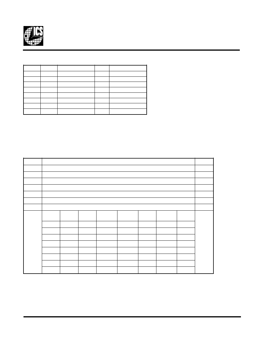
5
ICS9250-51
Byte 3: ICS Reserved Functionality and frequency select register (Default as noted in PWD)
Note 1: For system operation, the BSEL lines of the CPU will program FS0, FS2 for the appropriate CPU speed,
always with SDRAM = 100MHz. After BIOS verifies the SDRAM is PC133 speed, then bit 0 can be written
from the default 0 to 1 to change the SDRAM output frequency from 100MHz to 133MHz. This will only
change if the CPU is at the 133MHz FSB speed as shown in this table. The CPU, 3v66, PCI, and IOAPIC
clocks will be glitch free during this transition, and only SDRAM will change.
Note 2: "ICS RESERVED BITS" must be writtern as "O".
Note3: Undefined bits can be written either as "1 or 0"
t
i
B
n
o
i
t
p
i
t
c
s
e
D
D
W
P
7
t
i
B
)
2
e
t
o
N
(
t
i
b
d
e
v
r
e
s
e
R
S
C
I
0
6
t
i
B
)
2
e
t
o
N
(
t
i
b
d
e
v
r
e
s
e
R
S
C
I
0
5
t
i
B
)
2
e
t
o
N
(
t
i
b
d
e
v
r
e
s
e
R
S
C
I
0
4
t
i
B
)
2
e
t
o
N
(
t
i
b
d
e
v
r
e
s
e
R
S
C
I
0
3
t
i
B
)
2
e
t
o
N
(
t
i
b
d
e
v
r
e
s
e
R
S
C
I
0
2
t
i
B
)
3
e
t
o
N
(
t
i
b
d
e
n
i
f
e
d
n
U
X
1
t
i
B
)
3
e
t
o
N
(
t
i
b
d
e
n
i
f
e
d
n
U
X
0
t
i
B
0
t
i
B
0
S
F
1
S
F
K
L
C
U
P
C
z
H
M
M
A
R
D
S
z
H
M
6
6
V
3
z
H
M
K
L
C
I
C
P
z
H
M
C
I
P
A
O
I
z
H
M
0
1
e
t
o
N
0
0
0
6
6
.
6
6
0
.
0
0
1
6
6
.
6
6
3
3
.
3
3
3
3
.
3
3
0
1
0
0
.
0
0
1
0
.
0
0
1
6
6
.
6
6
3
3
.
3
3
3
3
.
3
3
0
0
1
2
3
.
3
3
1
2
3
.
3
3
1
6
6
.
6
6
3
3
.
3
3
3
3
.
3
3
0
1
1
2
3
.
3
3
1
0
.
0
0
1
6
6
.
6
6
3
3
.
3
3
3
3
.
3
3
1
0
0
6
6
.
6
6
0
.
0
0
1
6
6
.
6
6
3
3
.
3
3
3
3
.
3
3
1
1
0
0
.
0
0
1
0
.
0
0
1
6
6
.
6
6
3
3
.
3
3
3
3
.
3
3
1
0
1
2
3
.
3
3
1
2
3
.
3
3
1
6
6
.
6
6
3
3
.
3
3
3
3
.
3
3
1
1
1
2
3
.
3
3
1
2
3
.
3
3
1
6
6
.
6
6
3
3
.
3
3
3
3
.
3
3
Byte 2: Control Register
(1 = enable, 0 = disable)
Notes:
1. Inactive means outputs are held LOW and are disabled from switching. These outputs are designed to be
configured at power-on and are not expected to be configured during the normal modes of operation.
2. PWD = Power on Default
3. Undefined bit can be wirtten with either a "1" or "0".
t
i
B
#
n
i
P
e
m
a
N
D
W
P
n
o
i
t
p
i
r
c
s
e
D
7
t
i
B
9
)
P
G
A
(
2
-
6
6
V
3
1
)
e
v
i
t
c
a
n
I
/
e
v
i
t
c
A
(
6
t
i
B
0
2
5
K
L
C
I
C
P
1
)
e
v
i
t
c
a
n
I
/
e
v
i
t
c
A
(
5
t
i
B
9
1
4
K
L
C
I
C
P
1
)
e
v
i
t
c
a
n
I
/
e
v
i
t
c
A
(
4
t
i
B
8
1
3
K
L
C
I
C
P
1
)
e
v
i
t
c
a
n
I
/
e
v
i
t
c
A
(
3
t
i
B
6
1
2
K
L
C
I
C
P
1
)
e
v
i
t
c
a
n
I
/
e
v
i
t
c
A
(
2
t
i
B
5
1
1
K
L
C
I
C
P
1
)
e
v
i
t
c
a
n
I
/
e
v
i
t
c
A
(
1
t
i
B
3
1
0
K
L
C
I
C
P
1
)
e
v
i
t
c
a
n
I
/
e
v
i
t
c
A
(
0
t
i
B
-
t
i
b
d
e
n
i
f
e
d
n
U
X
)
e
v
i
t
c
a
n
I
/
e
v
i
t
c
A
(