9250-08
ICS9250-08
Third party brands and names are the property of their respective owners.
Integrated
Circuit
Systems, Inc.
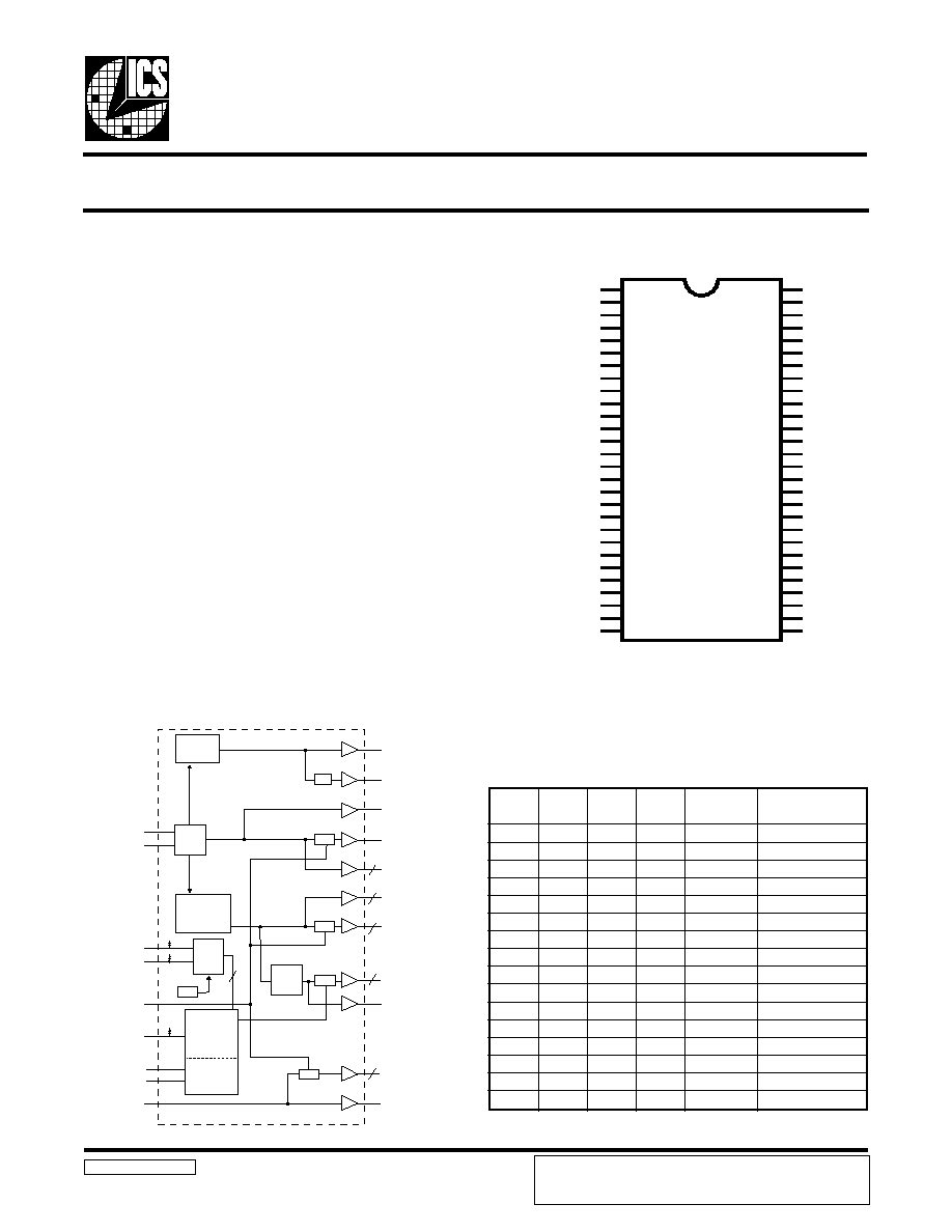
Block Diagram
Frequency Generator & Integrated Buffers for Celeron & P
II
/
III
TM
9250-08 Rev H 10/8/99
Functionality
Pin Configuration
Recommended Application:
BX, Appollo Pro 133 type of chip set.
Output Features:
·
3 - CPUs @2.5V, up to 150MHz.
·
17 - SDRAM @ 3.3V, up to 150MHz.
·
7 - PCI @3.3V
·
2 - IOAPIC @ 2.5V
·
1 - 48MHz, @3.3V fixed.
·
1 - 24MHz @ 3.3V
·
2 - REF @3.3V, 14.318MHz.
Features:
·
Up to 150MHz frequency support
·
Support power management: CPU, PCI, stop and Power
down Mode form I
2
C programming.
·
Spread spectrum for EMI control (0 to -0.5%, ± 0.25%).
·
Uses external 14.318MHz crystal
Key Specifications:
·
CPU CPU: <175ps
·
CPU PCI: min = 1ns max = 4ns
·
PCI PCI: <250ps
·
SDRAM - SDRAM: <500ps
56-Pin SSOP
* Internal Pull-up Resistor of 240K to 3.3V on indicated inputs
** Internal Pull-down resistor of 240K to GND on indicated inputs.
VDDREF
*
REF1
*PCI_STOP/REF0
GND
X1
X2
VDDPCI
*MODE/PCICLK_F
**FS3/PCICLK0
GND
VDDPCI
BUFFERIN
SDRAM11
SDRAM10
VDDSDR
SDRAM9
SDRAM8
GND
SDRAM15
SDRAM14
GND
SDATA
SCLK
PCICLK1
PCICLK2
PCICLK3
PCICLK4
PCICLK5
FS2/
VDDLIOAPIC
IOAPIC0
IOAPIC_F
GND
CPUCLK_F
CPUCLK1
VDDLCPU
CPUCLK2
GND
CPU_STOP#
SDRAM_F
VDDSDR
SDRAM0
SDRAM1
GND
SDRAM2
SDRAM3
SDRAM4
SDRAM5
VDDSDR
SDRAM6
SDRAM7
GND
SDRAM12
SDRAM13
VDD48
24MHz/FS0*
48MHz/FS1*
ICS9250-08
1
2
3
4
5
6
7
8
9
10
11
12
13
14
15
16
17
18
19
20
21
22
23
24
25
26
27
28
56
55
54
53
52
51
50
49
48
47
46
45
44
43
42
41
40
39
38
37
36
35
34
33
32
31
30
29
{
I C
2
3
S
F
2
S
F
1
S
F
0
S
F
U
P
C
)
z
H
M
(
)
z
H
M
(
K
L
C
I
C
P
1
1
1
1
3
3
1
)
4
/
U
P
C
(
3
.
3
3
1
1
1
0
4
2
1
)
4
/
U
P
C
(
1
3
1
1
0
1
0
5
1
)
4
/
U
P
C
(
5
.
7
3
1
1
0
0
0
4
1
)
4
/
U
P
C
(
5
3
1
0
1
1
5
0
1
)
3
/
U
P
C
(
5
3
1
0
1
0
0
1
1
)
3
/
U
P
C
(
7
6
.
6
3
1
0
0
1
5
1
1
)
3
/
U
P
C
(
3
3
.
8
3
1
0
0
0
0
2
1
)
3
/
U
P
C
(
0
0
.
0
4
0
1
1
1
3
.
0
0
1
)
3
/
U
P
C
(
3
4
.
3
3
0
1
1
0
3
3
1
)
3
/
U
P
C
(
3
3
.
4
4
0
1
0
1
2
1
1
)
3
/
U
P
C
(
3
3
.
7
3
0
1
0
0
3
0
1
)
2
/
U
P
C
(
3
3
.
4
3
0
0
1
1
8
.
6
6
)
2
/
U
P
C
(
0
4
.
3
3
0
0
1
0
3
.
3
8
)
2
/
U
P
C
(
5
6
.
1
4
0
0
0
1
5
7
)
2
/
U
P
C
(
5
.
7
3
0
0
0
0
4
2
1
)
2
/
U
P
C
(
3
3
.
1
4
CPU_STOP#
PCI_STOP#
PLL2
PLL1
Spread
Spectrum
48MHz
IOAPIC0
CPUCLK [2:1]
CPUCLK_F
IOAPIC_F
SDRAM [15:0]
SDRAM_F
PCICLK [5:0]
PCICLK_F
X1
X2
XTAL
OSC
PCI
CLOCK
DIVDER
STOP
STOP
÷2
STOP
STOP
POR
SDATA
SCLK
FS[3:0]
MODE
{
I C
2
Control
Logic
Config.
Reg.
REF [1:0]
24MHz
LATCH
1
2
2
16
6
6
4
BUFFERIN
ICS reserves the right to make changes in the device data identified in
this publication without further notice. ICS advises its customers to
obtain the latest version of all device data to verify that any
information being relied upon by the customer is current and accurate.

2
ICS9250-08
Third party brands and names are the property of their respective owners.
Pin Configuration
Notes:
1:
Bidirectional input/output pins, input logic levels are latched at internal power-on-reset. Use 10Kohm resistor
to program logic Hi to VDD or GND for logic low.
R
E
B
M
U
N
N
I
P
E
M
A
N
N
I
P
E
P
Y
T
N
O
I
T
P
I
R
C
S
E
D
2
1
F
E
R
T
U
O
t
u
p
t
u
o
k
c
o
l
c
e
c
n
e
r
e
f
e
r
z
H
M
8
1
3
.
4
1
2
S
F
1
N
I
I
C
P
D
D
V
o
t
p
u
-
l
l
u
p
s
a
H
.
t
u
p
n
i
t
c
e
l
e
s
y
c
n
e
u
q
e
r
f
d
e
h
c
t
a
L
3
0
F
E
R
T
U
O
t
u
p
t
u
o
k
c
o
l
c
e
c
n
e
r
e
f
e
r
z
H
M
8
1
3
.
4
1
#
P
O
T
S
_
I
C
P
1
N
I
.
w
o
l
n
e
h
w
l
e
v
e
l
"
0
"
c
i
g
o
l
t
a
]
0
:
5
[
K
L
C
I
C
P
s
t
l
a
H
)
0
=
E
D
O
M
,
e
l
i
b
o
m
n
i
(
,
2
4
,
4
3
,
6
2
,
3
2
,
0
1
,
4
3
5
,
8
4
D
N
G
R
W
P
.
d
n
u
o
r
G
5
1
X
N
I
.
)
F
p
3
3
l
a
n
i
m
o
n
(
,
p
a
c
d
a
o
l
l
a
n
r
e
t
n
i
s
a
H
.
t
u
p
n
i
z
H
M
8
1
3
.
4
1
6
2
X
T
U
O
k
c
a
b
d
e
e
f
d
n
a
)
F
p
3
3
(
p
a
c
d
a
o
l
l
a
n
r
e
t
n
i
s
a
H
.
t
u
p
t
u
o
l
a
t
s
y
r
C
1
X
o
t
r
o
t
s
i
s
e
r
8
F
_
K
L
C
I
C
P
T
U
O
#
P
O
T
S
_
I
C
P
y
b
d
e
t
c
e
f
f
a
t
o
n
k
c
o
l
c
S
U
B
g
n
i
n
n
u
r
e
e
r
F
E
D
O
M
1
N
I
n
e
h
w
#
P
O
T
S
_
I
C
P
o
t
3
n
i
p
s
t
r
e
v
n
o
C
.
t
c
e
l
e
s
E
D
O
M
r
o
f
t
u
p
n
i
d
e
h
c
t
a
L
.
t
n
e
m
e
g
a
n
a
m
r
e
w
o
p
r
o
f
w
o
l
9
3
S
F
1
N
I
n
w
o
d
-
l
l
u
p
,
t
u
p
n
i
t
c
e
l
e
s
y
c
n
e
u
q
e
r
f
d
e
h
c
t
a
L
0
K
L
C
I
C
P
T
U
O
#
P
O
T
S
_
I
C
P
y
b
d
e
t
c
e
f
f
a
t
o
n
k
c
o
l
c
S
U
B
g
n
i
n
n
u
r
e
e
r
F
1
1
,
2
1
,
3
1
,
4
1
,
6
1
]
1
:
5
[
K
L
C
I
C
P
T
U
O
.
s
t
u
p
t
u
O
k
c
o
l
C
I
C
P
7
1
N
I
R
E
F
F
U
B
N
I
s
r
e
f
f
u
B
r
o
f
t
u
p
n
I
7
2
A
T
A
D
S
N
I
I
(
.
t
r
o
p
g
i
f
n
o
c
l
a
i
r
e
s
r
o
f
n
i
a
t
a
d
l
a
i
r
e
S
2
)
C
8
2
K
L
C
S
N
I
I
(
.
t
r
o
p
g
i
f
n
o
c
l
a
i
r
e
s
r
o
f
t
u
p
n
i
k
c
o
l
C
2
)
C
0
3
z
H
M
4
2
T
U
O
.
D
F
r
o
O
/
I
r
e
p
u
S
r
o
f
t
u
p
t
u
o
k
c
o
l
c
z
H
M
4
2
0
S
F
1
N
I
.
4
D
D
V
o
t
p
u
-
l
l
u
p
s
a
H
.
t
u
p
n
i
t
c
e
l
e
s
y
c
n
e
u
q
e
r
f
d
e
h
c
t
a
L
9
2
z
H
M
8
4
T
U
O
.
B
S
U
r
o
f
t
u
p
t
u
o
k
c
o
l
c
z
H
M
8
4
1
S
F
1
N
I
.
2
D
D
V
o
t
p
u
-
l
l
u
p
s
a
H
.
t
u
p
n
i
t
c
e
l
e
s
y
c
n
e
u
q
e
r
f
d
e
h
c
t
a
L
,
0
2
,
5
1
,
7
,
1
,
1
3
5
4
,
7
3
,
F
E
R
D
D
V
,
I
C
P
D
D
V
8
4
D
D
V
,
R
D
S
D
D
V
R
W
P
.
n
o
i
t
c
n
u
f
r
o
f
s
p
u
o
r
g
r
e
w
o
p
e
e
s
,
y
l
p
p
u
s
r
e
w
o
p
V
3
.
3
l
a
n
i
m
o
N
,
8
1
,
3
3
,
2
3
,
5
2
,
4
2
,
6
3
,
5
3
,
2
2
,
1
2
,
9
1
,
3
4
,
1
4
,
0
4
,
9
3
,
8
3
4
4
]
0
:
5
1
[
M
A
R
D
S
T
U
O
s
k
c
o
l
c
M
A
R
D
S
6
4
F
_
M
A
R
D
S
T
U
O
#
P
O
T
S
_
U
P
C
y
b
d
e
t
c
e
f
f
a
t
o
N
k
c
o
l
c
M
A
R
D
S
g
n
i
n
n
u
r
e
e
r
F
7
4
#
P
O
T
S
_
U
P
C
N
I
K
L
C
U
P
C
s
t
l
a
H
]
0
:
5
1
[
M
A
R
D
S
,
0
C
I
P
A
O
I
,
]
1
:
2
[
.
w
o
l
n
e
h
w
l
e
v
e
l
"
0
"
c
i
g
o
l
t
a
s
k
c
o
l
c
6
5
,
0
5
,
U
P
C
L
D
D
V
C
I
P
A
O
I
L
D
D
V
R
W
P
.
l
a
n
i
m
o
n
V
5
.
2
,
y
l
p
p
u
s
r
e
w
o
p
r
e
f
f
u
b
k
c
o
l
c
C
I
P
A
O
I
d
n
a
U
P
C
5
5
0
C
I
P
A
O
I
T
U
O
C
I
P
A
O
I
L
D
D
V
y
b
d
e
r
e
w
o
P
)
z
H
M
8
1
3
.
4
1
(
.
t
u
p
t
u
o
k
c
o
l
c
C
I
P
A
O
I
9
4
,
1
5
]
1
:
2
[
K
L
C
U
P
C
T
U
O
)
z
H
M
6
.
6
6
r
o
0
6
(
2
L
D
D
V
y
b
d
e
r
e
w
o
P
.
s
k
c
o
l
c
t
u
p
t
u
O
U
P
C
2
5
F
_
K
L
C
U
P
C
T
U
O
.
#
P
O
T
S
_
U
P
C
e
h
t
y
t
d
e
t
c
e
f
f
a
t
o
N
.
k
c
o
l
c
t
u
p
t
u
o
U
P
C
g
n
i
n
n
u
r
e
e
r
F
4
5
F
_
C
I
P
A
O
I
T
U
O
g
n
i
n
n
u
r
e
e
r
F
.
t
u
p
t
u
o
k
c
o
l
c
C
I
P
A
O
I
#
P
O
T
S
_
U
P
C
e
h
t
y
b
d
e
t
c
e
f
f
a
t
o
N
C
I
P
A
O
I
L
D
D
V
y
b
d
e
r
e
w
o
P
)
z
H
M
8
1
8
1
3
.
4
1
(

3
ICS9250-08
Third party brands and names are the property of their respective owners.
General Description
The ICS9250-08 is the single chip clock solution for Desktop/
designs using BX, Appollo Pro 133 type of chip sets. It provides
all necessary clock signals for such a system.
Spread spectrum may be enabled through I
2
C programming.
Spread spectrum typically reduces system EMI by 8dB to
10dB. This simplifies EMI qualification without resorting to
board design iterations or costly shielding. The ICS9250-08
employs a proprietary closed loop design, which tightly
controls the percentage of spreading over process and
temperature variations.
Serial programming I
2
C interface allows changing functions,
stop clock programming and frequency selection.
Power Groups
VDDREF = REF [1:0], X1, X2
VDDPCI = PCICLK_F, PCICLK [5:0]
VDDSDR = SDRAM [15:0], supply for PLL core,
VDD48 = 48MHz, 24MHz
VDDLIOAPIC = IOAPIC_F
VDDLCPU = CPUCLK_F [2:1]
Mode Pin - Power Management Input Control
E
D
O
M
)
t
u
p
n
I
d
e
h
c
t
a
L
(
0
#
P
O
T
S
_
I
C
P
)
t
u
p
n
I
(
1
0
F
E
R
)
t
u
p
t
u
O
(
4
ICS9250-08
Third party brands and names are the property of their respective owners.
1.
The ICS clock generator is a slave/receiver, I
2
C component. It can read back the data stored in the latches for
verification. Read-Back will support Intel PIIX4 "Block-Read" protocol.
2.
The data transfer rate supported by this clock generator is 100K bits/sec or less (standard mode)
3.
The input is operating at 3.3V logic levels.
4.
The data byte format is 8 bit bytes.
5.
To simplify the clock generator I
2
C interface, the protocol is set to use only "Block-Writes" from the controller. The
bytes must be accessed in sequential order from lowest to highest byte with the ability to stop after any complete byte
has been transferred. The Command code and Byte count shown above must be sent, but the data is ignored for those
two bytes. The data is loaded until a Stop sequence is issued.
6.
At power-on, all registers are set to a default condition, as shown.
General I
2
C serial interface information
The information in this section assumes familiarity with I
2
C programming.
For more information, contact ICS for an I
2
C programming application note.
How to Write:
Controller (host) sends a start bit.
Controller (host) sends the write address D2
(H)
ICS clock will acknowledge
Controller (host) sends a dummy command code
ICS clock will acknowledge
Controller (host) sends a dummy byte count
ICS clock will acknowledge
Controller (host) starts sending first byte (Byte 0)
through byte 5
ICS clock will acknowledge each byte one at a time.
Controller (host) sends a Stop bit
How to Read:
Controller (host) will send start bit.
Controller (host) sends the read address D3
(H)
ICS clock will acknowledge
ICS clock will send the byte count
Controller (host) acknowledges
ICS clock sends first byte (Byte 0) through byte 5
Controller (host) will need to acknowledge each byte
Controller (host) will send a stop bit
Notes:
Controller (Host)
ICS (Slave/Receiver)
Start Bit
Address
D3
(H)
ACK
Byte Count
ACK
Byte 0
ACK
Byte 1
ACK
Byte 2
ACK
Byte 3
ACK
Byte 4
ACK
Byte 5
ACK
Stop Bit
How to Read:
Controller (Host)
ICS (Slave/Receiver)
Start Bit
Address
D2
(H)
ACK
Dummy Command Code
ACK
Dummy Byte Count
ACK
Byte 0
ACK
Byte 1
ACK
Byte 2
ACK
Byte 3
ACK
Byte 4
ACK
Byte 5
ACK
Stop Bit
How to Write:

5
ICS9250-08
Third party brands and names are the property of their respective owners.
t
i
B
n
o
i
t
p
i
r
c
s
e
D
D
W
P
7
t
i
B
n
o
i
t
a
l
u
d
o
M
m
u
r
t
c
e
p
S
d
a
e
r
p
S
%
5
2
.
0
±
-
0
n
o
i
t
a
l
u
d
o
M
m
u
r
t
c
e
p
S
d
a
e
r
p
S
%
5
.
0
±
-
1
0
4
t
i
B
5
t
i
B
6
t
i
B
2
t
i
B
k
c
o
l
c
U
P
C
I
C
P
1
e
t
o
N
,
2
t
i
B
4
:
6
t
i
B
1
1
1
0
0
1
1
0
3
.
0
0
1
3
3
1
)
3
/
U
P
C
(
3
4
.
3
3
)
3
/
U
P
C
(
3
3
.
4
4
1
0
1
0
0
0
1
0
2
1
1
3
0
1
)
3
/
U
P
C
(
3
3
.
7
3
)
3
/
U
P
C
(
3
.
4
3
1
1
0
0
0
1
0
0
8
.
6
6
3
.
3
8
)
2
/
U
P
C
(
4
.
3
3
)
2
/
U
P
C
(
5
6
.
1
4
1
0
0
0
0
0
0
0
5
7
4
2
1
)
2
/
U
P
C
(
5
.
7
3
)
3
/
U
P
C
(
3
3
.
1
4
1
1
1
1
0
1
1
1
3
3
1
4
2
1
)
4
/
U
P
C
(
5
2
.
3
3
)
4
/
U
P
C
(
0
0
.
1
3
1
0
1
1
0
0
1
1
0
5
1
0
4
1
)
4
/
U
P
C
(
0
5
.
7
3
)
4
/
U
P
C
(
0
0
.
5
3
1
1
0
1
0
1
0
1
5
0
1
0
1
1
)
3
/
U
P
C
(
0
0
.
5
3
)
3
/
U
P
C
(
7
6
.
6
3
1
0
0
1
0
0
0
1
5
1
1
0
2
1
)
3
/
U
P
C
(
3
3
.
8
3
)
3
/
U
P
C
(
0
0
.
0
4
3
t
i
B
s
t
u
p
n
I
d
e
h
c
t
a
L
,
t
c
e
l
e
s
e
r
a
w
d
r
a
h
y
b
d
e
t
c
e
l
e
s
s
i
y
c
n
e
u
q
e
r
F
-
0
)
e
v
o
b
a
(
4
:
6
,
2
t
i
B
y
b
d
e
t
c
e
l
e
s
s
i
y
c
n
e
u
q
e
r
F
-
1
0
1
t
i
B
l
a
m
r
o
N
-
0
)
d
a
e
r
p
S
r
e
t
n
e
C
(
d
e
l
b
a
n
E
m
u
r
t
c
e
p
S
d
a
e
r
p
S
-
1
0
0
t
i
B
g
n
i
n
n
u
R
-
0
s
t
u
p
t
u
o
l
l
a
e
t
a
t
s
i
r
T
-
1
0
Byte0: Functionality and Frequency Select Register (default = 0)
Serial Configuration Command Bitmap
Note: PWD = Power-Up Default
Note 1. Default at Power-up will be for latched logic inputs to define frequency. Bits 2, 4, 5,
6 are default to 0000, and if bit 3 is written to a 1 to use Bits 2, 6:4, then these
should be defined to desired frequency at same write cycle.