Äîêóìåíòàöèÿ è îïèñàíèÿ www.docs.chipfind.ru
General Description
Features
ICS932S200
Integrated
Circuit
Systems, Inc.
0427C--07/03/02
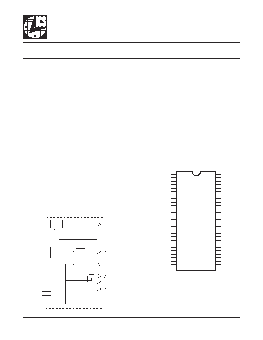
Block Diagram
Frequency Timing Generator for Dual Server/Workstation Systems
Pin Configuration
56-pin 300 mil SSOP
56-pin 240 mil TSSOP
·
Generates the following system clocks:
- 6 CPU clocks ( 2.5V, 100/133MHz)
- 6 PCI clocks, including 1 free running(3.3V,
33MHz)
- 3 IOAPIC clocks (2.5V, 16.67MHz)
- 2 Fixed frequency 66MHz clocks(3.3V, 66MHz)
- 2 REF clocks(3.3V, 14.318MHz)
- 1 USB clock (3.3V, 48MHz)
·
Efficient power management through PD#,
CPU_STOP# and PCI_STOP#.
·
0.5% typical down spread modulation on CPU, PCI,
IOAPIC and 3V66 output clocks.
·
Uses external 14.318MHz crystal.
The ICS932S200 is a dual CPU clock generator for
serverworks HE-T, HE-SL-T, LE-T chipsets for P III type
processors in a Dual-CPU system. Single ended CPU
clocks provide faster than 1.5V/ns transition times by
parallel connection of 2 CPU pins to each processor.
Spread Spectrum may be enabled by driving the
SPREAD# pin active. Spread spectrum typically
reduces system EMI by 8dB to 10dB. This simplifies
EMI qualification without resorting to board design
iterations or costly shielding. The ICS932S200 employs
a proprietary closed loop design, which tightly controls
the percentage of spreading over process and
temperature variations.
Key Specification:
·
CPU Output Jitter: 150ps
·
IOAPIC Output Jitter: 250ps
·
3V66, PCI Output Jitter: 250ps
·
CPU Output Skew: <175ps
·
PCI Output Skew: <500ps
·
3V66 Output Skew <250ps
·
IOAPIC Output Skew <250ps
·
CPU to 3V66 Output Offset: 0 - 1.5ns (CPU leads)
·
CPU to PCI Output Offset: 1.5 - 4.0ns (CPU leads)
·
CPU to APIC Output Offset: 1.5 - 4.0ns (CPU
leads)
PCICLK_F
PLL2
PLL1
Spread
Spectrum
48MHz
CPUCLK (5:0)
IOAPIC (2:0)
3V66 (1:0)
PCICLK (4:0)
5
3
2
6
2
X1
X2
XTAL
OSC
CPU
DIVDER
IOAPIC
DIVDER
3V66
DIVDER
PCI
DIVDER
Stop
PD#
PCI_STOP#
CPU_STOP#
SPREAD#
SEL 133/100#
SEL0
SEL1
Control
Logic
Config.
Reg.
REF (1:0)
GND
REF0
REF1
VDD
X1
X2
GND
GND
PCICLK_F
VDD
PCICLK0
PCICLK1
GND
PCICLK2
PCICLK3
VDD
VDD
PCICLK4
GND
GND
GND
VDD
VDD
GND
3V66_0
3V66_1
VDD
SEL 133/100#
VDDL
IOAPIC2
IOAPIC1
IOAPIC0
GND
VDDL
CPUCLK5
CPUCLK4
GND
VDDL
CPUCLK3
CPUCLK2
GND
VDDL
CPUCLK1
CPUCLK0
GND
VDD
GND
PCI_STOP#
CPU_STOP#
PD#
SPREAD#
SEL1
SEL0
VDD
48MHz
GND
ICS932S200
1
2
3
4
5
6
7
8
9
10
11
12
13
14
15
16
17
18
19
20
21
22
23
24
25
26
27
28
56
55
54
53
52
51
50
49
48
47
46
45
44
43
42
41
40
39
38
37
36
35
34
33
32
31
30
29
2
ICS932S200
0427C--07/03/02
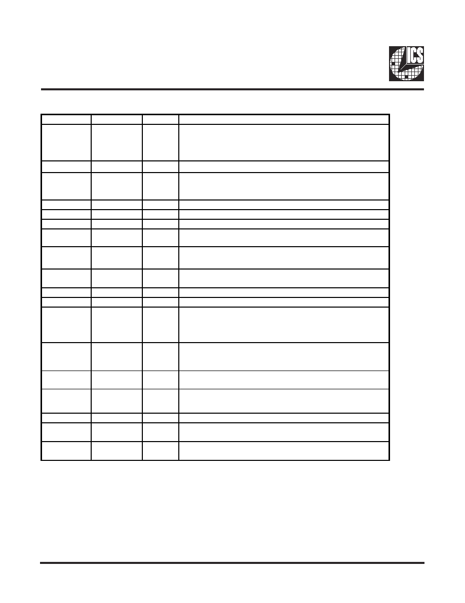
Pin Descriptions
Pin number
Pin name
Type
Description
1, 7, 8, 13, 19
20, 21, 24, 29,
38, 40, 44, 48,
52
GND
PWR
Gnd pins
3, 2
REF(1:0)
OUT
14.318MHz reference clock outputs at 3.3V
4,. 10, 16, 17,
22, 23, 27, 31,
39
VDD
PWR
Power pins 3.3V
5
X1
IN
XTAL_IN 14.318MHz crystal input
6
X2
OUT
XTAL_OUT Crystal output
9
PCICLK_F
OUT
Free running PCI clock not affected by PCI_STOP#
18, 15, 14,
12, 11
PCICLK (4:0)
OUT
PCI clock outputs at 3.3V. Synchronous to CPU clocks.
26, 25
3V66 (1:0)
OUT
66MHz outputs at 3.3V. These outputs are stopped when CPU_STOP# is
driven active..
28
SEL 133/100#
IN
This selects the frequency for the CPU and CPU/2 outputs. High =
133MHz, Low=100MHz
30
48MHz
OUT
Fixed 48MHz clock output. 3.3V
33, 32
SEL (1:0)
IN
Function select pins. See truth table for details.
34
SPREAD#
IN
Enables spread spectrum when active(Low). modulates all the CPU, PCI,
IOAPIC and 3V66 clocks. Does not affect the REF and 48MHz clocks.
0.5% down spread modulation.
35
PD#
IN
This asynchronous input powers down the chip when drive active(Low).
The internal PLLs are disabled and all the output clocks are held at a Low
state.
36
CPU_STOP#
IN
This asychronous input halts the CPUCLK and the 3V66 clocks at logic "0"
when driven active(Low).
37
PCI_STOP#
IN
This asynchronous input halts the PCICLK at logic"0" when driven
active(Low). PCICLK_F is not affected by this input.
43, 47, 51, 56
VDDL
PWR
Power pins 2.5V
50, 49, 46,
45, 42, 41
CPUCLK (5:0)
OUT
Host bus clock output at 2.5V. 133MHz or 100MHz depending on the state
of the SEL 133/100MHz.
55, 54, 53
IOAPIC (2:0)
OUT
IOAPIC clocks at 2.5V. Synchronous with CPUCLKs but fixed at
16.67MHz.
3
ICS932S200
0427C--07/03/02
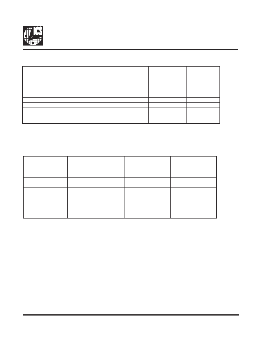
Frequency Select:
Note:
1. TCLK is a test clock driven on the x1 input during test mode.
ICS932S200 Power Management Features:
Note:
1. LOW means outputs held static LOW as per latency requirement next page.
2. On means active.
3. PD# pulled Low, impacts all outputs including REF and 48 MHz outputs.
4. All 3V66 as well as all CPLU clocks should stop cleanly when CPU_STOP# is pulled LOW.
5. IOAPIC, REF, 48 MHz signals are not controlled by the CPU_STOP# functionality and are enabled all in all conditions
except PD# = LOW
L
E
S
#
0
0
1
/
3
3
1
1
L
E
S
0
L
E
S
U
P
C
z
H
M
6
6
V
3
z
H
M
I
C
P
z
H
M
8
4
z
H
M
F
E
R
z
H
M
C
I
P
A
O
I
z
H
M
s
t
n
e
m
m
o
C
0
0
0
Z
-
i
H
Z
-
i
H
Z
-
i
H
Z
-
i
H
Z
-
i
H
Z
-
i
H
e
t
a
t
s
-
i
r
T
0
0
1
A
/
N
A
/
N
A
/
N
A
/
N
A
/
N
A
/
N
d
e
v
r
e
s
e
R
0
1
0
0
0
1
6
.
6
6
3
.
3
3
Z
-
i
H
8
1
3
.
4
1
7
6
.
6
1
L
L
P
z
H
M
8
4
d
e
l
b
a
s
i
d
0
1
1
0
0
1
6
.
6
6
3
.
3
3
0
.
8
4
8
1
3
.
4
1
7
6
.
6
1
1
0
0
2
/
K
L
C
T
4
/
K
L
C
T
8
/
K
L
C
T
2
/
K
L
C
T
K
L
C
T
6
1
/
K
L
C
T
)
1
(
e
d
o
m
t
s
e
T
1
0
1
A
/
N
A
/
N
A
/
N
A
/
N
A
/
N
A
/
N
d
e
v
r
e
s
e
R
1
1
0
3
3
1
6
.
6
6
3
.
3
3
Z
-
i
H
8
1
3
.
4
1
7
6
.
6
1
1
1
1
3
3
1
6
.
6
6
3
.
3
3
0
.
8
4
8
1
3
.
4
1
7
6
.
6
1
#
P
O
T
S
_
U
P
C
#
D
P
#
P
O
T
S
_
I
C
P
K
L
C
U
P
C
C
I
P
A
O
I
6
6
V
3
I
C
P
F
_
I
C
P
.
F
E
R
z
H
M
8
4
c
s
O
s
O
C
V
X
0
X
W
O
L
W
O
L
W
O
L
W
O
L
W
O
L
W
O
L
F
F
O
F
F
O
0
1
0
W
O
L
N
O
W
O
L
W
O
L
N
O
N
O
N
O
N
O
0
1
1
W
O
L
N
O
W
O
L
N
O
N
O
N
O
N
O
N
O
1
1
0
N
O
N
O
N
O
W
O
L
N
O
N
O
N
O
N
O
1
1
1
N
O
N
O
N
O
N
O
N
O
N
O
N
O
N
O
4
ICS932S200
0427C--07/03/02
Power Management Requirements:
Note:
1. Clock on/off latency is defined in the number of rising edges of free running PCICLKs between the clock disable goes
low/high to the first valid clock comes out of the device.
2. Power up latency is when PWR_DWN# goes inactive (high to when the first valid clocks are dirven from the device.
l
a
g
n
i
S
e
t
a
t
S
l
a
g
n
i
S
y
c
n
e
t
a
L
f
o
s
e
g
d
e
g
n
i
s
i
r
f
o
.
o
N
K
L
C
I
C
P
P
O
T
S
_
U
P
C
)
d
e
l
b
a
s
i
d
(
0
1
)
d
e
l
b
a
n
e
(
1
1
#
P
O
T
S
_
I
C
P
)
d
e
l
b
a
s
i
d
(
0
1
)
d
e
l
b
a
n
e
(
1
1
#
D
P
)
n
o
i
t
a
r
e
p
o
l
a
m
r
o
n
(
1
S
m
3
)
n
w
o
d
r
e
w
o
p
(
0
.
x
a
m
2
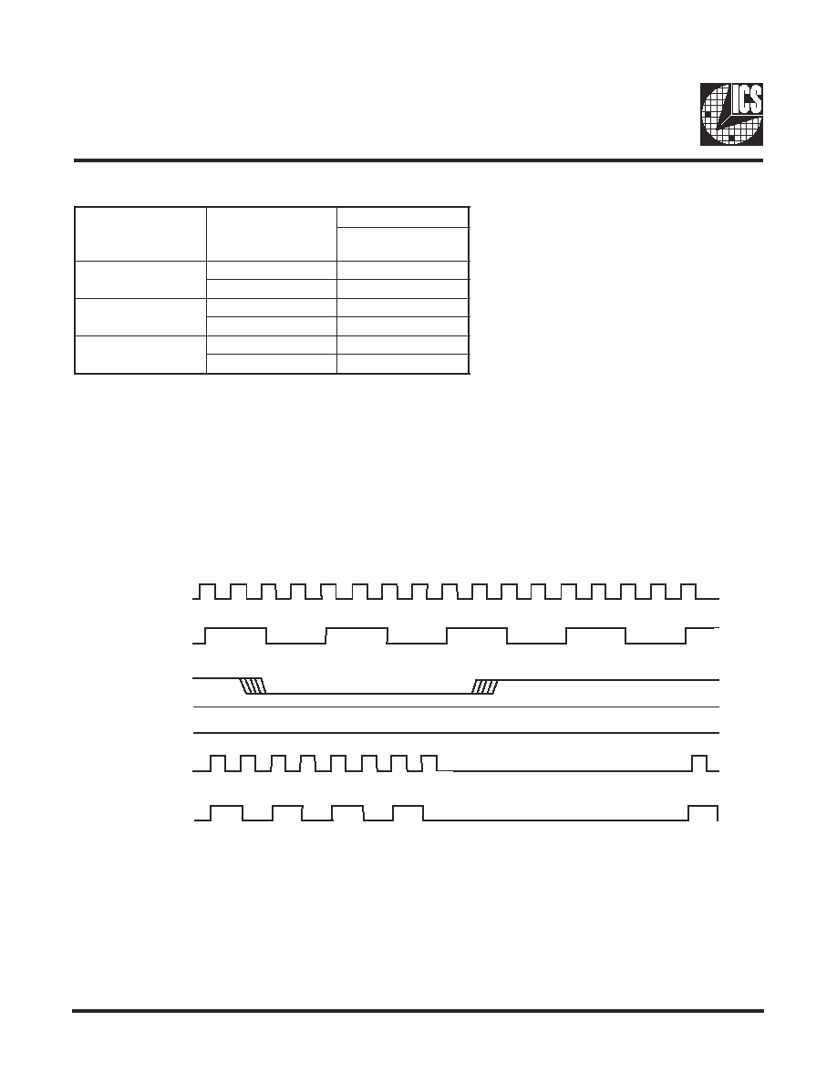
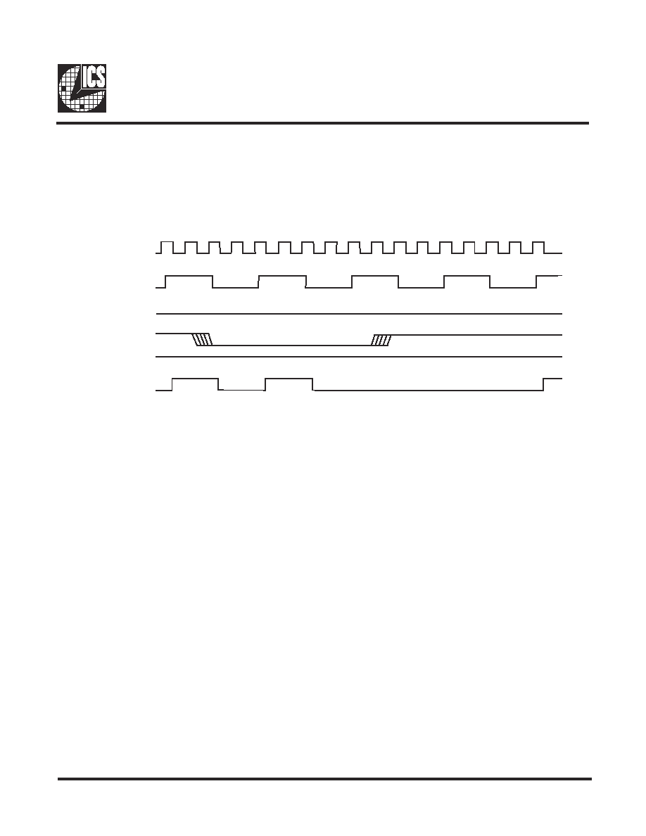
CPU_STOP# Timing Diagram
CPU_STOP# is an asynchronous input to the clock synthesizer. It is used to turn off the CPU and 3V66 clocks for
low power operation. CPU_STOP# is asserted asynchronously by the external clock control logic with the rising edge
of free running PCI clock (and hence CPU clock) and must be internally synchronized to the external output. All other
clocks will continue to run while the CPU clocks are disabled. The CPU clocks must always be stopped in a low state
and started in such a manner as to guarantee that the high pulse width is a full pulse.
Notes:
1. All timing is referenced to the internal CPUCLK.
2. The internal label means inside the chip and is a reference only.
This in fact may not be the way that the control is designed.
3. 3V66 clocks also stop/start before
4. PD# and PCI_STOP# are shown in a high state.
5. Diagrams shown with respect to 133MHz. Similar operation when
CPU is 100MHz
CPUCLK
(internal)
(internal)
(externall)
(externall)
PCICLK
PCI_STOP#
CPU_STOP#
PD#
CPUCLK
3V66
5
ICS932S200
0427C--07/03/02
PCI_STOP# Timing Diagram
PCI_STOP# is an input to the clock synthesizer and must be made synchronous to the clock driver PCICLK_F output.
It is used to turn off the PCI clocks for low power operation. PCI clocks are required to be stopped in a low state and
started such that a full high pulse width is guaranteed. ONLY one rising edge of PCICLK_F is allowed after the clock
control logic switched for the PCI outputs to become enabled/disabled.
Notes:
1. All timing is referenced to CPUCLK.
2. Internal means inside the chip.
3. All other clocks continue to run undisturbed.
4. PD# and CPU_STOP# are shown in a high state.
5. Diagrams shown with respect to 133MHz. Similar operation when CPU is 100MHz.
CPUCLK
(internal)
(internal)
(externall)
PCICLK
PCI_STOP#
CPU_STOP#
PD#
PCICLK