 | ÐлекÑÑоннÑй компоненÑ: ICS9341 | СкаÑаÑÑ:  PDF PDF  ZIP ZIP |
Äîêóìåíòàöèÿ è îïèñàíèÿ www.docs.chipfind.ru
Integrated
Circuit
Systems, Inc.
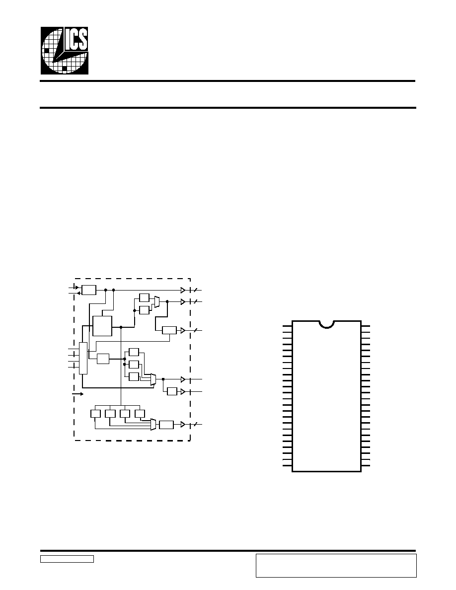
General Description
Features
ICS9341
Block Diagram
133MHz Clock Generator and Integrated Buffer for PowerPCTM
9341 Rev A 10/12/99
Pin Configuration
48-pin SSOP
* Internal pull-up resistor of 120K to 3.3V on
indicated inputs
** Internal pull-down resistor of 120K to GND
on indicated inputs.
Generates the following system clocks:
- 4-CPUA (3.3V, up to 133MHz)
- 4-CPUB (3.3V, up to 133MHz)
- 8-PCI (3.3V, 33.3MHz)
- 1-OUT (3.3v, 64MHz)
- 1-OUT/2 (3.3V, OUT/2MHz)
- 2-REF (3.3V, 14.318MHz)
Up to 133MHz frequency support.
Stop clocks for power management
Spread Spectrum for EMI control
±.25% center spread
Skew characteristics:
- CPU - CPU: <350ps
- CPU - PCI: <500ps
- PCI - PCI: <500ps
The ICS9341 generates all clocks required for high speed
PowerPC RISC microprocessor systems. Generating clocks in
phase with an external reference frequency.
Spread Spectrum may be enabled by driving the SS_EN pin
active. Spread spectrum typically reduces system EMI by 8dB
to 10dB. This simplifies EMI qualification without resorting to
board design iterations or costly shielding. The ICS9341
employs a proprietary closed loop design, which tightly
controls the percentage of spreading over process and
temperature variations.
Power Groups:
VDDREF, GNDREF = REF, X1, X2
GNDPCI, VDDPCI = PCICLK
VDD66, GND66 = 3V66
VDD48, GND48 = 48MHz
VDDCOR, GNDCOR = PLL Core
VDDLCPU/2 , GNDLCPU/2 = CPU/2
VDDLIOAPIC, GNDIOAPIC = IOAPIC
PD#
CPUB_STOP#
OUT_SEL (0:1)
PCI_STOP#
SS_EN
X1
X2
OSC
PLL
Spread
Spectrum
REF (0:1)
2
4
4
OUT
OUT/2
CPUCLKB (1:4)
CPUCLKA (1:4)
STOP
C
o
n
t
r
o
l
/ 2
PLL2
8
PCICLK (1:8)
STOP
/ 8
/ 6
/ 5
/ 4
/ 2
/ 4
/ 5
/ 6
/ 3
GNDREF
X1
X2
VDDPCI
PCICLK1
PCICLK2
PCICLK3
PCICLK4
GNDPCI
GNDCPUB
CPUB1
CPUB2
CPUB3
CPUB4
VDDCPUB
VDDPCI
PCICLK5
PCICLK6
PCICLK7
PCICLK8
FS0
FS1
*OUT_SEL0
GNDPCI
REF1
REF0
VDDREF
CPUA1
CPUA2
SS_EN
GNDCPUA
OUT_SEL1*
PD#
VDDCPUA
CPUA3
CPUA4
CPUB_STOP#**
VDDD
VDDOUT
OUT
OUT/2
GNDOUT
GNDA
GNDD
N/C
N/C
*PCI_STOP#
VDDA
ICS9341
1
2
3
4
5
6
7
8
9
10
11
12
13
14
15
16
17
18
19
20
21
22
23
24
48
47
46
45
44
43
42
41
40
39
38
37
36
35
34
33
32
31
30
29
28
27
26
25
ICS reserves the right to make changes in the device data identified in
this publication without further notice. ICS advises its customers to
obtain the latest version of all device data to verify that any
information being relied upon by the customer is current and accurate.
2
ICS9341
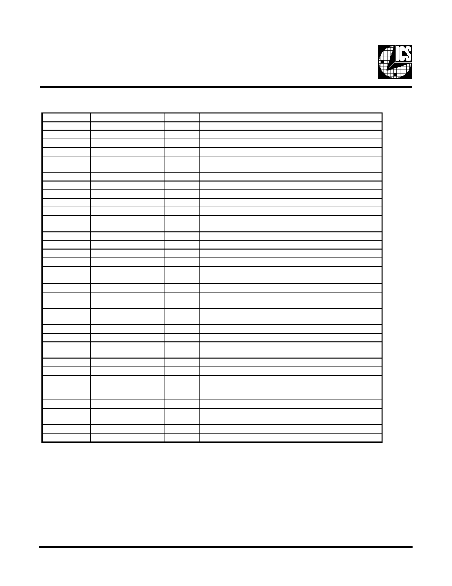
Pin Descriptions
Pin number
Pin name
Type
D escription
1
G N D REF
PWR
G round pin for REF clocks.
2
X 1
IN
X TA L_IN 14.318M H z crystal input.
3
X 2
O U T
X TA L_O U T Crystal output.
4, 16
V D D PCI
PWR
3.3V olts pow er pin for PCICLK s.
5, 6, 7, 8, 17, 18,
19, 20
PCICLK (1:8)
O U T
PCI clock output at 3.3V . Synchronous to CPU clocks.
9, 24
G N D PCI
PWR
G round pin for PCI clocks.
10
G N D CPU B
PWR
G round pin for CPU B clocks.
11, 12, 13, 14
CPU B (1:4)
O U T
CPU CLK outputs up to 133.3M H z.
15
V D D CPU B
PWR
Pow er pin for the CPU bank B CLK s. 3.3V .
21, 22
FS (0:1)
IN
Logic - input for frequency selection.
23, 41
*O U T_SEL (0:1)
IN
These control the output functionality of the O U T and O U T/2 pins.
Refer to table for details.
24
G N D PCI
PWR
G nd pin for PCICLK s.
25
V D D A
PWR
Pow er for analog outputs.
26
*PCI_STO P#
IN
This active low input stops PCI clocks.
27, 28
N /C
-
N ot connected
29
G N D D
PWR
D igitial ground
30
G N D A
PWR
A nalog ground
31
G N D O U T
PWR
G round for output pins.
32
O U T/2
O U T
H alf the O U T frequency. D ependent on O U T_SEL. Refer to table
for details.
33
O U T
O U T
This output frequency is dependent on O U T_SEL. Refer to table for
details.
34
V D D O U T
PWR
Pow er for O U T pins 3.3V .
35
V D D D
PWR
Pow er for digitial outputs.
36
CPU B_STO P#**
IN
This active low input stops the CPU B clocks at a logic "0" level
w hen input low .
45, 44, 38, 37
CPU A (1:4)
O U T
CPU CLK outputs up to 133.3M H z.
39
V D D CPU A
PWR
Pow er pin for the CPU bank A CLK s. 3.3V .
40
PD #
IN
This asynchronous input pow ers dow n the chip w hen drive
active(Low ). The internal PLLs are disabled and all the output clocks
are held at a Low state.
42
G N D CPU A
PWR
G round pin for CPU B clocks.
43
SS_EN
IN
Spread spectrum is turned on by driving this input high and turned
off by driving low .
46
V D D REF
PWR
Pow er pin for REF clocks.
47, 48
REF
O U T
14.318M H z reference clock outputs at 3.3V .
3
ICS9341
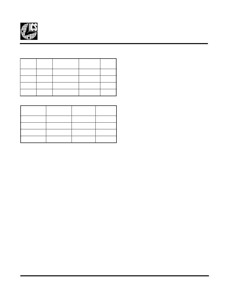
Frequency Selection
1
S
F
0
S
F
B
U
P
C
,
A
U
P
C
)
z
H
M
(
I
C
P
)
z
H
M
(
F
E
R
)
z
H
M
(
1
1
3
.
3
3
1
3
.
3
3
8
1
3
.
4
1
1
0
0
0
1
3
.
3
3
8
1
3
.
4
1
0
1
3
.
3
8
3
.
3
3
8
1
3
.
4
1
0
0
6
.
6
6
3
.
3
3
8
1
3
.
4
1
1
L
E
S
_
T
U
O
0
L
E
S
_
T
U
O
T
U
O
)
z
H
M
(
2
/
T
U
O
)
z
H
M
(
1
1
8
4
4
2
1
0
0
4
0
2
0
1
4
6
2
3
0
0
d
e
p
p
o
t
S
d
e
p
p
o
t
S
4
ICS9341
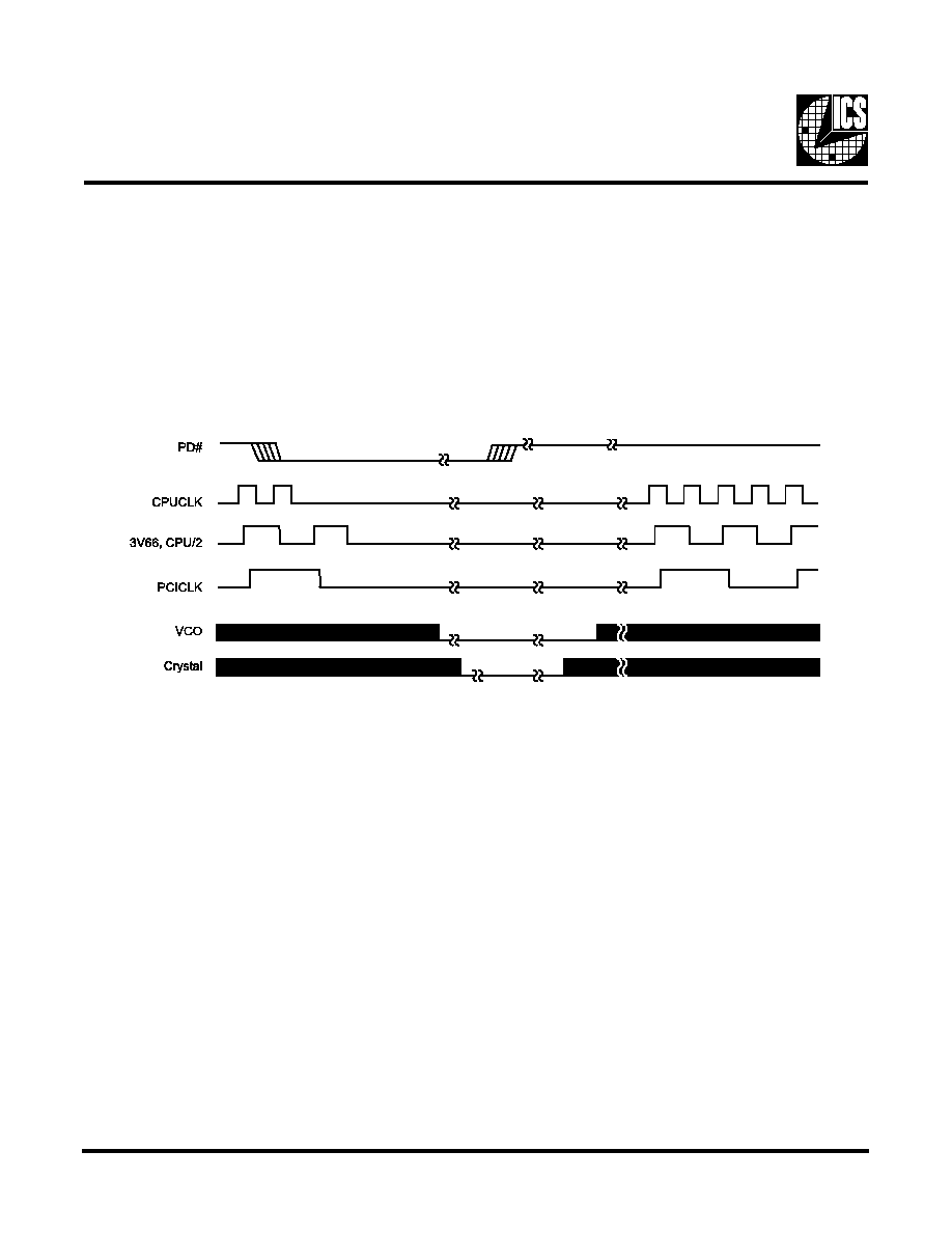
PD# Timing Diagram
The power down selection is used to put the part into a very low power state without turning off the power to the part. PD# is
an asynchronous active low input. This signal needs to be synchronized internal to the device prior to powering down the clock
synthesizer.
Internal clocks are not running after the device is put in power down. When PD# is active low all clocks need to be driven to a
low value and held prior to turning off the VCOs and crystal. The power up latency needs to be less than 3 mS. The power down
latency should be as short as possible but conforming to the sequence requirements shown below. The REF and 48MHz clocks
are expected to be stopped in the LOW state as soon as possible. Due to the state of the internal logic, stopping and holding
the REF clock outputs in the LOW state may require more than one clock cycle to complete.
Notes:
1. All timing is referenced to the Internal CPUCLK (defined as inside the ICS9341 device).
2. As shown, the outputs Stop Low on the next falling edge after PD# goes low.
3. PD# is an asynchronous input and metastable conditions may exist. This signal is synchronized inside this part.
4. The shaded sections on the VCO and the Crystal signals indicate an active clock.
5. Diagrams shown with respect to 133MHz. Similar operation when CPU is 100MHz.
5
ICS9341
PCI_STOP# Timing Diagram
PCI_STOP# is an input to the clock synthesizer. It is used to turn off the PCI clocks for low power operation. PCI clocks are
required to be stopped in a low state and started such that a full high pulse width is guaranteed. ONLY one rising edge of
PCICLK_F is allowed after the clock control logic switched for the PCI outputs to become enabled/disabled.
Notes:
1. All timing is referenced to CPUCLK.
2. Internal means inside the chip.
3. All other clocks continue to run undisturbed.
4. PD# and CPU_STOP# are shown in a high state.
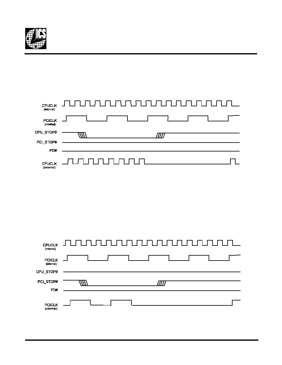
CPU_STOP# Timing Diagram
CPU_STOP# is an asynchronous input to the clock synthesizer. It is used to turn off the CPU and 3V66 clocks for low power
operation. CPU_STOP# is asserted asynchronously by the external clock control logic with the rising edge of free running PCI
clock (and hence CPU clock) and must be internally synchronized to the external output. All other clocks will continue to run
while the CPU clocks are disabled. The CPU clocks must always be stopped in a low state and started in such a manner as to
guarantee that the high pulse width is a full pulse.
Notes:
1. All timing is referenced to the internal CPUCLK.
2. The internal label means inside the chip and is a reference only. This in fact may not be the way that the control is designed.
3. PD# and PCI_STOP# are shown in a high state.