9250-08
Integrated
Circuit
Systems, Inc.
ICS9342
Third party brands and names are the property of their respective owners.
9342 Rev E 9/06/00
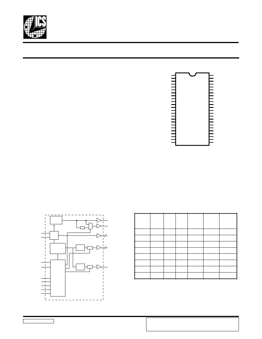
Pin Configuration
48-Pin 300mil SSOP
Recommended Application:
Power PC System Clock
Output Features:
·
12- CPUs @ 3.3V, up to 146MHz
·
1- PCIREF @ 3.3V, up to 73MHz
·
1 - OUT 3.3V, 64MHz
·
1 - OUT/2 3.3V, OUT/2MHz
·
2 - REF @ 3.3V, 14.318MHz
Features:
·
Up to 146MHz frequency support
·
Support power management: CPU, PCI stop and power
down mode.
·
Spread spectrum for EMI control (0 to -0.5%, ± 0.25%).
·
Uses external 14.318MHz crystal
·
FS pins for frequency select
·
Support for industrial temperature range (-40C° to 85C°)
Key Specifications:
·
CPU Output Skew: <200ps
·
CPU - PCI Output Skew: <500ps
·
CPU Output Jitter: <150ps
·
PCI Output Jitter: <500ps
133MHz Clock Generator and Integrated Buffer for PowerPCTM
VDDREF
REF1
REF0
GNDREF
X1
X2
*PD#
*CPU-STOP#
VDD
GND
*PCI_STOP#
*SS_EN#
VDDPCI
PCIREF
GNDPCI
*FS0
*FS1
*FS2
VDDFP
GNDFP
*TEST#/OUT
*BOOST#/OUT_DIV2
*PDFP#
VDDA
OUTSEL1*
VDDCPU
GNDCPU
CPU0
CPU1
CPU2
VDDCPU
GNDCPU
CPU3
CPU4
CPU5
VDDCPU
GNDCPU
CPU6
CPU7
CPU8
VDDCPU
GNDCPU
CPU9
CPU10
CPU11
VDDCPU
GNDCPU
OUTSEL0*
ICS9342
1
2
3
4
5
6
7
8
9
10
11
12
13
14
15
16
17
18
19
20
21
22
23
24
48
47
46
45
44
43
42
41
40
39
38
37
36
35
34
33
32
31
30
29
28
27
26
25
* Internal pull-up resistor of 120K to VDD
on indicated inputs.
Functionality
Block Diagram
SS_EN#
OUTSEL (1:0)
PLL2
PLL1
Spread
Spectrum
OUT
OUT/DIV2
CPUCLK (11:0)
12
2
PCIREF
X1
X2
XTAL
OSC
CPU
DIVDER
PCI
DIVDER
Stop
Stop
FS (2:0)
PD#
PDFP#
TEST#
BOOST#
Control
Logic
Config.
Reg.
/ 2
REF (1:0)
T
S
E
T
2
S
F
1
S
F
0
S
F
U
P
C
z
H
M
I
C
P
z
H
M
F
E
R
z
H
M
1
1
1
1
3
3
.
3
3
1
3
3
.
3
3
8
1
3
.
4
1
1
1
1
0
0
0
.
0
0
1
3
3
.
3
3
8
1
3
.
4
1
1
1
0
1
3
3
.
3
8
3
3
.
3
3
8
1
3
.
4
1
1
1
0
0
6
6
.
6
6
3
3
.
3
3
8
1
3
.
4
1
1
0
1
1
3
3
.
3
3
1
6
6
.
6
6
8
1
3
.
4
1
1
0
1
0
0
0
.
0
0
1
6
6
.
6
6
8
1
3
.
4
1
1
0
0
1
3
3
.
3
8
6
6
.
6
6
8
1
3
.
4
1
1
0
0
0
6
6
.
6
6
6
6
.
6
6
8
1
3
.
4
1
ICS reserves the right to make changes in the device data identified in
this publication without further notice. ICS advises its customers to
obtain the latest version of all device data to verify that any
information being relied upon by the customer is current and accurate.
2
ICS9342
Third party brands and names are the property of their respective owners.
Pin Configuration
General Description
The ICS9342 generates all clocks required for high speed PowerPC RISC microprocessor systems. With a zero delay buffer
chip such as the ICS9112-17 multiple PCI clock outputs can be generated in phase with PCIREF.
Spread Spectrum may be enabled by driving the SS_EN# pin low. Spread spectrum typically reduces system EMI by 8dB to
10dB. This simplifies EMI qualification without resorting to board design iterations or costly shielding. The ICS9342
employs a proprietary closed loop design, which tightly controls the percentage of spreading over process and temperature
variations.
PIN NUMBER
PIN NAME
TYPE
DESCRIPTION
1
VDDREF
PWR
Ref(1:0), XTAL power supply, nominal 3.3V
2,3
REF[1:0]
OU T
14.318 M Hz reference clocks
4
GNDREF
PWR
Ground pin for the REF outputs
5
X1
IN
Crystal input,nominally 14.318M Hz.
6
X2
OU T
Crystal output, nominally 14.318M Hz.
7
PD#
IN
Pow ers down chip, active low .
8
CPU_STOP#
IN
Stops all CPUCLKs [11:0] at logic 0 level, w hen input low
9
VDD
PWR
3.3V power for the digital core.
10
GND
PWR
Ground pin for the digital core.
11
PCI_STO P#
IN
Drives PCIREF to logic 0 level, when input low
12
SS_EN#
IN
Spread spectrum is turned on by driving this input low and turned off by
driving it high.
13
VDDPCI
PWR
Pow er supply for PCIREF, nominal 3.3V.
14
PCIREF
OU T
Reference clock for PCI Zero Delay Buffer.
15
GNDPCI
PWR
Ground pin for PCIREF.
18, 17, 16
FS (2:0)
IN
Frequency select pins.
19
VDDFP
PWR
3.3V power for the Fixed PLL core.
20
GNDFP
PER
Ground pin for the Fixed PLL core.
O UT
OU T
3.3V O UT reference clock.
TEST#
IN
Logic input to select over clocking or under clocking frequencies.
(latched input)
OUT_D IV2
OU T
3.3V 1/2 frequency OUT reference clock.
BOOST#
IN
Logic input to select normal or test mode frequencies. (latched input)
23
PDFP#
IN
Pow ers down Fixed PLL. When driven to low, OUT and OUT_DIV2 clocks
will be stopped
24
VDDA
PWR
3.3V power for the PLL core
48, 25
OUTSEL(1:0)
IN
Frequency select pins for OUT and OUT_DIV2 clocks.
26, 31, 36, 41, 46
GNDCPU
PWR
Ground pin for CPU clocks.
27, 32, 37, 42, 47
VDDCPU
PWR
3.3V power supply for CPU clocks.
21
22
3
ICS9342
Third party brands and names are the property of their respective owners.
Frequency Selection
1
L
E
S
_
T
U
O
0
L
E
S
_
T
U
O
T
U
O
)
z
H
M
(
2
V
I
D
_
T
U
O
)
z
H
M
(
F
E
R
)
z
H
M
(
1
1
8
4
4
2
8
1
3
.
4
1
1
0
0
4
0
2
8
1
3
.
4
1
0
1
4
6
2
3
8
1
3
.
4
1
0
0
8
4
#
8
4
8
1
3
.
4
1
#
T
S
O
O
B
#
T
S
E
T
2
S
F
1
S
F
0
S
F
U
P
C
z
H
M
I
C
P
z
H
M
F
E
R
z
H
M
E
U
L
A
V
/
E
P
Y
T
S
S
d
e
l
b
a
n
e
S
S
f
I
X
1
1
1
1
3
3
.
3
3
1
3
3
.
3
3
8
1
3
.
4
1
d
a
e
r
p
S
n
w
o
D
%
5
.
0
-
o
t
0
X
1
1
1
0
0
0
.
0
0
1
3
3
.
3
3
8
1
3
.
4
1
d
a
e
r
p
S
n
w
o
D
%
5
.
0
-
o
t
0
X
1
1
0
1
3
3
.
3
8
3
3
.
3
3
8
1
3
.
4
1
d
a
e
r
p
S
n
w
o
D
%
5
.
0
-
o
t
0
X
1
1
0
0
6
6
.
6
6
3
3
.
3
3
8
1
3
.
4
1
d
a
e
r
p
S
n
w
o
D
%
5
.
0
-
o
t
0
X
1
0
1
1
3
3
.
3
3
1
6
6
.
6
6
8
1
3
.
4
1
d
a
e
r
p
S
n
w
o
D
%
5
.
0
-
o
t
0
X
1
0
1
0
0
0
.
0
0
1
6
6
.
6
6
8
1
3
.
4
1
d
a
e
r
p
S
n
w
o
D
%
5
.
0
-
o
t
0
X
1
0
0
1
3
3
.
3
8
6
6
.
6
6
8
1
3
.
4
1
d
a
e
r
p
S
n
w
o
D
%
5
.
-
o
t
0
X
1
0
0
0
6
6
.
6
6
6
6
.
6
6
8
1
3
.
4
1
d
a
e
r
p
S
n
w
o
D
%
5
.
0
-
o
t
0
1
0
1
1
1
2
6
.
6
4
1
6
.
6
3
8
1
3
.
4
1
d
a
e
r
p
S
r
e
t
n
e
C
%
5
2
.
0
+
1
0
1
1
0
9
9
.
9
0
1
6
.
6
3
8
1
3
.
4
1
d
a
e
r
p
S
r
e
t
n
e
C
%
5
2
.
0
+
1
0
1
0
1
8
5
.
1
9
6
.
6
3
8
1
3
.
4
1
d
a
e
r
p
S
r
e
t
n
e
C
%
5
2
.
0
+
1
0
1
0
0
1
3
.
3
7
6
.
6
3
8
1
3
.
4
1
d
a
e
r
p
S
r
e
t
n
e
C
%
5
2
.
0
+
1
0
0
1
1
2
6
.
6
4
1
3
.
3
7
8
1
3
.
4
1
d
a
e
r
p
S
r
e
t
n
e
C
%
5
2
.
0
+
1
0
0
1
0
9
9
.
9
0
1
3
.
3
7
8
1
3
.
4
1
d
a
e
r
p
S
r
e
t
n
e
C
%
5
2
.
0
+
1
0
0
0
1
8
5
.
1
9
3
.
3
7
8
1
3
.
4
1
d
a
e
r
p
S
r
e
t
n
e
C
%
5
2
.
0
+
1
0
0
0
0
1
3
.
3
7
3
.
3
7
8
1
3
.
4
1
d
a
e
r
p
S
r
e
t
n
e
C
%
5
2
.
0
+
0
0
1
1
1
8
9
.
9
1
1
0
0
.
0
3
8
1
3
.
4
1
d
a
e
r
p
S
r
e
t
n
e
C
%
5
2
.
0
+
0
0
1
1
0
0
0
.
0
9
0
0
.
0
3
8
1
3
.
4
1
d
a
e
r
p
S
r
e
t
n
e
C
%
5
2
.
0
+
0
0
1
0
1
3
9
.
4
7
0
0
.
0
3
8
1
3
.
4
1
d
a
e
r
p
S
r
e
t
n
e
C
%
5
2
.
0
+
0
0
1
0
0
8
/
f
e
R
=
I
C
P
,
4
/
f
e
R
=
U
P
C
,
e
d
o
M
t
s
e
T
0
0
0
1
1
8
9
.
9
1
1
0
0
.
0
6
8
1
3
.
4
1
d
a
e
r
p
S
r
e
t
n
e
C
%
5
2
.
0
+
0
0
0
1
0
0
0
.
0
9
0
0
.
0
6
8
1
3
.
4
1
d
a
e
r
p
S
r
e
t
n
e
C
%
5
2
.
0
+
0
0
0
0
1
3
9
.
4
7
0
0
.
0
6
8
1
3
.
4
1
d
a
e
r
p
S
r
e
t
n
e
C
%
5
2
.
0
+
0
0
0
0
0
s
t
u
p
t
u
o
l
l
a
,
e
t
a
t
s
i
r
T
4
ICS9342
Third party brands and names are the property of their respective owners.
Absolute Maximum Ratings
Supply Voltage . . . . . . . . . . . . . . . . . . . . . . . . . . . . 7.0 V
Logic Inputs . . . . . . . . . . . . . . . . . . . . . . . . . . . . . . GND 0.5 V to V
DD
+0.5 V
Ambient Operating Temperature . . . . . . . . . . . . . -40°C to +85°C
Storage Temperature . . . . . . . . . . . . . . . . . . . . . . . 65°C to +150°C
Stresses above those listed under Absolute Maximum Ratings may cause permanent damage to the device. These ratings are
stress specifications only and functional operation of the device at these or any other conditions above those listed in the
operational sections of the specifications is not implied. Exposure to absolute maximum rating conditions for extended
periods may affect product reliability.
Electrical Characteristics - Input/Supply/Common Output Parameters
T
A
= 0 - 70º C; Supply Voltage V
D D
= 3.3 V +/-5% (unles s otherwis e s tated)
PARAM ETER
SYM BOL
CONDITIONS
M IN
TYP
M AX
UNITS
Input High Voltage
V
IH
2
V
DD
+0.3
V
Input Low Voltage
V
IL
V
SS
-0.3
0.8
V
Input High Current
I
IH
V
IN
= V
DD
0.1
5
µ
A
Input Low Current
I
IL1
V
IN
= 0 V; Inputs with no pull-up resistors
-5
2.0
µ
A
Input Low Current
I
IL2
V
IN
= 0 V; Inputs with pull-up resistors
-200
-100
µ
A
I
DD3.3 OP6 6
Select @ 66M Hz; M ax discrete cap loads
134
175
Operating
I
DD3.3 OP8 3
Select @ 83M Hz; M ax discrete cap loads
165
200
Supply Current
I
DD3 .3OP1 0 0
Select @ 100M Hz; M ax discrete cap loads
198
225
I
DD3 .3OP1 3 3
Select @ 133M Hz; M ax discrete cap loads
254
300
Power Down
Supply Current
Input frequency
F
i
V
DD
= 3.3 V
12
14.318
16
M Hz
C
IN
Logic Inputs
5
pF
C
INX
X1 & X2 pins
13.5
18
22.5
pF
Transition Time
1
T
Tran s
To 1st crossing of target Freq.
3
ms
Settling Time
1
T
S
From 1st crossing to 1% target Freq.
1
ms
Clk Stabilization
1
T
STAB
From V
DD
= 3.3 V to 1% target Freq.
3
ms
Skew
1
t
CP U -P CI
V
T
= 1.5 V
190
500
ps
Input Capacitance
1
mA
PD# = 0
I
D D 3 .3 P D
313
400
µ
A
5
ICS9342
Third party brands and names are the property of their respective owners.
Electrical Characteristics - PCI
T
A
= 0 - 70º C; V
DD
= 3.3 V +/-5%; C
L
=30 pF
PARAMETER
SYMBOL
CONDITIONS
MIN
TYP
MAX
UNITS
Output Impedance
R
DSP1
1
V
O
= V
DD
*(0.5)
12
21
55
Output Impedance
R
DSN1
1
V
O
= V
DD
*(0.5)
12
21.2
55
Output High Voltage
V
OH1
I
OH
= -11 mA
2.4
Output Low Voltage
V
OL1
I
OL
= 9.4 mA
0.17
0.4
V
Output High Current
I
OH1
V
OH
= 2.0 V
-60
-22
mA
Output Low Current
I
OL1
V
OL
= 0.8 V
25
47
mA
Rise Time
1
t
r1
V
OL
= 0.4 V, V
OH
= 2.4 V
0.5
1
2
ns
Fall Time
1
t
f1
V
OH
= 2.4 V, V
OL
= 0.4 V
0.5
0.9
2
ns
Duty Cycle
1
d
t1
V
T
= 1.5 V
45
50
55
%
Jitter, Cycle-to-cycle
1
t
jcyc-cyc1
V
T
= 1.5 V
170
500
ps
1
Guaranteed by design, not 100% tested in production.
Electrical Characteristics - CPU
T
A
= 0 - 70º C; V
DD
= 3.3 V +/-5%; C
L
= 20 pF (unless otherwise stated)
PARAM ETER
SYM BOL
CONDITIONS
M IN
TYP
M AX
UNITS
Output Impedance
R
D SP 2 B
1
V
O
= V
D D
*(0.5)
13.5
20
45
Output Impedance
R
D SN 2 B
1
V
O
= V
D D
*(0.5)
13.5
29
45
Output High Voltage
V
OH2 B
I
OH
= -8.0 mA
2
2.4
V
Output Low Voltage
V
OL2 B
I
OL
= 12 mA
0.32
0.4
V
Output High Current
I
OH2 B
V
OH
=1.7 V
-37
-16
mA
Output Low C urrent
I
OL2B
V
OL
= 0.7 V
19
26
mA
Rise Time
t
r2 B
1
V
OL
= 0.4 V, V
OH
= 2.4 V
1.13
2
ns
Fall Time
t
f2 B
1
V
OH
= 2.4 V, V
OL
= 0.4 V
1.27
2
ns
VT = 1.5 V; Cpu@ 66M , 83M , 100M
45
52
56
VT = 1.5 V; Cpu@133M & 146.6M
51
56
60
Skew
t
sk 2 B
1
VT = 1.5 V
187
200
ps
VT = 1.5 V; Normal
95
150
VT = 1.5 V; Spread, CPU = 91.58M Hz
143
200
VT = 1.5 V; Spread, CPU remaining freq.
143
175
1
Guaranteed by design, not 100% tested in production.
Duty Cy cle
d
t2 B
1
%
Jitter, Cycle-to-cycle
tj
cy c-cyc2 B
1
ps