
Integrated
Circuit
Systems, Inc.
ICS9342
Third party brands and names are the property of their respective owners.
9342 Rev E 9/06/00
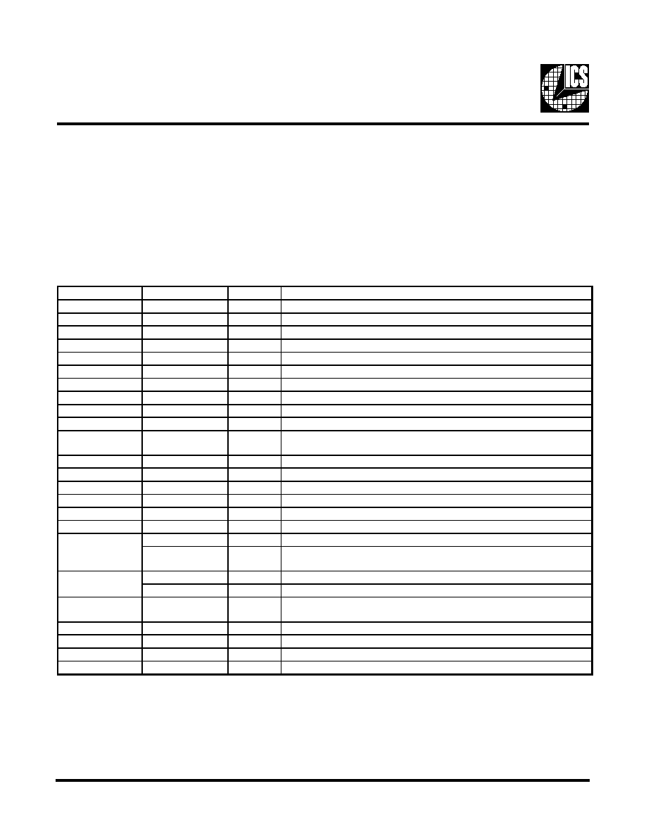
Pin Configuration
48-Pin 300mil SSOP
Recommended Application:
Power PC System Clock
Output Features:
∑
12- CPUs @ 3.3V, up to 146MHz
∑
1- PCIREF @ 3.3V, up to 73MHz
∑
1 - OUT 3.3V, 64MHz
∑
1 - OUT/2 3.3V, OUT/2MHz
∑
2 - REF @ 3.3V, 14.318MHz
Features:
∑
Up to 146MHz frequency support
∑
Support power management: CPU, PCI stop and power
down mode.
∑
Spread spectrum for EMI control (0 to -0.5%, ± 0.25%).
∑
Uses external 14.318MHz crystal
∑
FS pins for frequency select
∑
Support for industrial temperature range (-40C∞ to 85C∞)
Key Specifications:
∑
CPU Output Skew: <200ps
∑
CPU - PCI Output Skew: <500ps
∑
CPU Output Jitter: <150ps
∑
PCI Output Jitter: <500ps
133MHz Clock Generator and Integrated Buffer for PowerPCTM
VDDREF
REF1
REF0
GNDREF
X1
X2
*PD#
*CPU-STOP#
VDD
GND
*PCI_STOP#
*SS_EN#
VDDPCI
PCIREF
GNDPCI
*FS0
*FS1
*FS2
VDDFP
GNDFP
*TEST#/OUT
*BOOST#/OUT_DIV2
*PDFP#
VDDA
OUTSEL1*
VDDCPU
GNDCPU
CPU0
CPU1
CPU2
VDDCPU
GNDCPU
CPU3
CPU4
CPU5
VDDCPU
GNDCPU
CPU6
CPU7
CPU8
VDDCPU
GNDCPU
CPU9
CPU10
CPU11
VDDCPU
GNDCPU
OUTSEL0*
ICS9342
1
2
3
4
5
6
7
8
9
10
11
12
13
14
15
16
17
18
19
20
21
22
23
24
48
47
46
45
44
43
42
41
40
39
38
37
36
35
34
33
32
31
30
29
28
27
26
25
* Internal pull-up resistor of 120K to VDD
on indicated inputs.
Functionality
Block Diagram
SS_EN#
OUTSEL (1:0)
PLL2
PLL1
Spread
Spectrum
OUT
OUT/DIV2
CPUCLK (11:0)
12
2
PCIREF
X1
X2
XTAL
OSC
CPU
DIVDER
PCI
DIVDER
Stop
Stop
FS (2:0)
PD#
PDFP#
TEST#
BOOST#
Control
Logic
Config.
Reg.
/ 2
REF (1:0)
T
S
E
T
2
S
F
1
S
F
0
S
F
U
P
C
z
H
M
I
C
P
z
H
M
F
E
R
z
H
M
1
1
1
1
3
3
.
3
3
1
3
3
.
3
3
8
1
3
.
4
1
1
1
1
0
0
0
.
0
0
1
3
3
.
3
3
8
1
3
.
4
1
1
1
0
1
3
3
.
3
8
3
3
.
3
3
8
1
3
.
4
1
1
1
0
0
6
6
.
6
6
3
3
.
3
3
8
1
3
.
4
1
1
0
1
1
3
3
.
3
3
1
6
6
.
6
6
8
1
3
.
4
1
1
0
1
0
0
0
.
0
0
1
6
6
.
6
6
8
1
3
.
4
1
1
0
0
1
3
3
.
3
8
6
6
.
6
6
8
1
3
.
4
1
1
0
0
0
6
6
.
6
6
6
6
.
6
6
8
1
3
.
4
1
ICS reserves the right to make changes in the device data identified in
this publication without further notice. ICS advises its customers to
obtain the latest version of all device data to verify that any
information being relied upon by the customer is current and accurate.
2
ICS9342
Third party brands and names are the property of their respective owners.
Pin Configuration
General Description
The ICS9342 generates all clocks required for high speed PowerPC RISC microprocessor systems. With a zero delay buffer
chip such as the ICS9112-17 multiple PCI clock outputs can be generated in phase with PCIREF.
Spread Spectrum may be enabled by driving the SS_EN# pin low. Spread spectrum typically reduces system EMI by 8dB to
10dB. This simplifies EMI qualification without resorting to board design iterations or costly shielding. The ICS9342
employs a proprietary closed loop design, which tightly controls the percentage of spreading over process and temperature
variations.
PIN NUMBER
PIN NAME
TYPE
DESCRIPTION
1
VDDREF
PWR
Ref(1:0), XTAL power supply, nominal 3.3V
2,3
REF[1:0]
OU T
14.318 M Hz reference clocks
4
GNDREF
PWR
Ground pin for the REF outputs
5
X1
IN
Crystal input,nominally 14.318M Hz.
6
X2
OU T
Crystal output, nominally 14.318M Hz.
7
PD#
IN
Pow ers down chip, active low .
8
CPU_STOP#
IN
Stops all CPUCLKs [11:0] at logic 0 level, w hen input low
9
VDD
PWR
3.3V power for the digital core.
10
GND
PWR
Ground pin for the digital core.
11
PCI_STO P#
IN
Drives PCIREF to logic 0 level, when input low
12
SS_EN#
IN
Spread spectrum is turned on by driving this input low and turned off by
driving it high.
13
VDDPCI
PWR
Pow er supply for PCIREF, nominal 3.3V.
14
PCIREF
OU T
Reference clock for PCI Zero Delay Buffer.
15
GNDPCI
PWR
Ground pin for PCIREF.
18, 17, 16
FS (2:0)
IN
Frequency select pins.
19
VDDFP
PWR
3.3V power for the Fixed PLL core.
20
GNDFP
PER
Ground pin for the Fixed PLL core.
O UT
OU T
3.3V O UT reference clock.
TEST#
IN
Logic input to select over clocking or under clocking frequencies.
(latched input)
OUT_D IV2
OU T
3.3V 1/2 frequency OUT reference clock.
BOOST#
IN
Logic input to select normal or test mode frequencies. (latched input)
23
PDFP#
IN
Pow ers down Fixed PLL. When driven to low, OUT and OUT_DIV2 clocks
will be stopped
24
VDDA
PWR
3.3V power for the PLL core
48, 25
OUTSEL(1:0)
IN
Frequency select pins for OUT and OUT_DIV2 clocks.
26, 31, 36, 41, 46
GNDCPU
PWR
Ground pin for CPU clocks.
27, 32, 37, 42, 47
VDDCPU
PWR
3.3V power supply for CPU clocks.
21
22
3
ICS9342
Third party brands and names are the property of their respective owners.
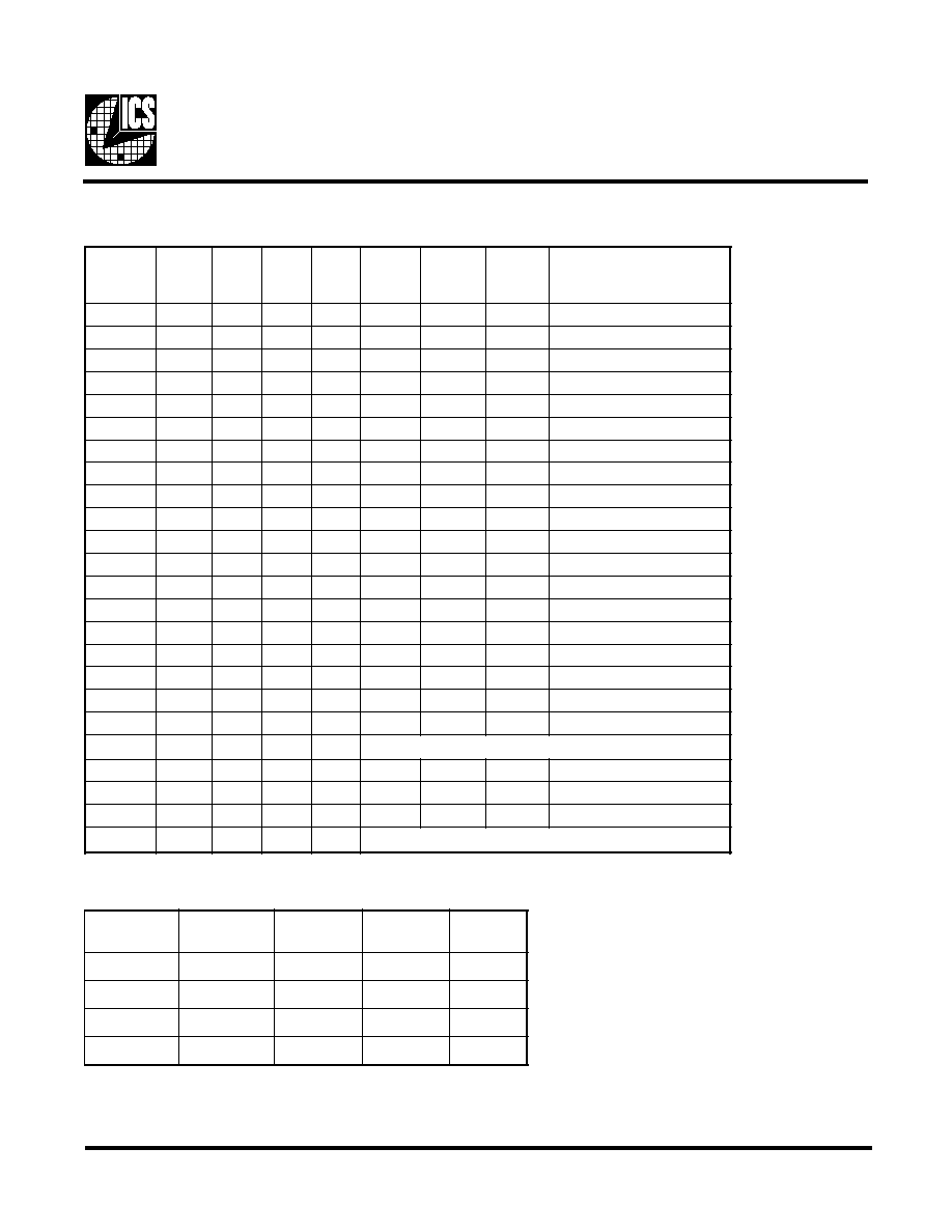
Frequency Selection
1
L
E
S
_
T
U
O
0
L
E
S
_
T
U
O
T
U
O
)
z
H
M
(
2
V
I
D
_
T
U
O
)
z
H
M
(
F
E
R
)
z
H
M
(
1
1
8
4
4
2
8
1
3
.
4
1
1
0
0
4
0
2
8
1
3
.
4
1
0
1
4
6
2
3
8
1
3
.
4
1
0
0
8
4
#
8
4
8
1
3
.
4
1
#
T
S
O
O
B
#
T
S
E
T
2
S
F
1
S
F
0
S
F
U
P
C
z
H
M
I
C
P
z
H
M
F
E
R
z
H
M
E
U
L
A
V
/
E
P
Y
T
S
S
d
e
l
b
a
n
e
S
S
f
I
X
1
1
1
1
3
3
.
3
3
1
3
3
.
3
3
8
1
3
.
4
1
d
a
e
r
p
S
n
w
o
D
%
5
.
0
-
o
t
0
X
1
1
1
0
0
0
.
0
0
1
3
3
.
3
3
8
1
3
.
4
1
d
a
e
r
p
S
n
w
o
D
%
5
.
0
-
o
t
0
X
1
1
0
1
3
3
.
3
8
3
3
.
3
3
8
1
3
.
4
1
d
a
e
r
p
S
n
w
o
D
%
5
.
0
-
o
t
0
X
1
1
0
0
6
6
.
6
6
3
3
.
3
3
8
1
3
.
4
1
d
a
e
r
p
S
n
w
o
D
%
5
.
0
-
o
t
0
X
1
0
1
1
3
3
.
3
3
1
6
6
.
6
6
8
1
3
.
4
1
d
a
e
r
p
S
n
w
o
D
%
5
.
0
-
o
t
0
X
1
0
1
0
0
0
.
0
0
1
6
6
.
6
6
8
1
3
.
4
1
d
a
e
r
p
S
n
w
o
D
%
5
.
0
-
o
t
0
X
1
0
0
1
3
3
.
3
8
6
6
.
6
6
8
1
3
.
4
1
d
a
e
r
p
S
n
w
o
D
%
5
.
-
o
t
0
X
1
0
0
0
6
6
.
6
6
6
6
.
6
6
8
1
3
.
4
1
d
a
e
r
p
S
n
w
o
D
%
5
.
0
-
o
t
0
1
0
1
1
1
2
6
.
6
4
1
6
.
6
3
8
1
3
.
4
1
d
a
e
r
p
S
r
e
t
n
e
C
%
5
2
.
0
+
1
0
1
1
0
9
9
.
9
0
1
6
.
6
3
8
1
3
.
4
1
d
a
e
r
p
S
r
e
t
n
e
C
%
5
2
.
0
+
1
0
1
0
1
8
5
.
1
9
6
.
6
3
8
1
3
.
4
1
d
a
e
r
p
S
r
e
t
n
e
C
%
5
2
.
0
+
1
0
1
0
0
1
3
.
3
7
6
.
6
3
8
1
3
.
4
1
d
a
e
r
p
S
r
e
t
n
e
C
%
5
2
.
0
+
1
0
0
1
1
2
6
.
6
4
1
3
.
3
7
8
1
3
.
4
1
d
a
e
r
p
S
r
e
t
n
e
C
%
5
2
.
0
+
1
0
0
1
0
9
9
.
9
0
1
3
.
3
7
8
1
3
.
4
1
d
a
e
r
p
S
r
e
t
n
e
C
%
5
2
.
0
+
1
0
0
0
1
8
5
.
1
9
3
.
3
7
8
1
3
.
4
1
d
a
e
r
p
S
r
e
t
n
e
C
%
5
2
.
0
+
1
0
0
0
0
1
3
.
3
7
3
.
3
7
8
1
3
.
4
1
d
a
e
r
p
S
r
e
t
n
e
C
%
5
2
.
0
+
0
0
1
1
1
8
9
.
9
1
1
0
0
.
0
3
8
1
3
.
4
1
d
a
e
r
p
S
r
e
t
n
e
C
%
5
2
.
0
+
0
0
1
1
0
0
0
.
0
9
0
0
.
0
3
8
1
3
.
4
1
d
a
e
r
p
S
r
e
t
n
e
C
%
5
2
.
0
+
0
0
1
0
1
3
9
.
4
7
0
0
.
0
3
8
1
3
.
4
1
d
a
e
r
p
S
r
e
t
n
e
C
%
5
2
.
0
+
0
0
1
0
0
8
/
f
e
R
=
I
C
P
,
4
/
f
e
R
=
U
P
C
,
e
d
o
M
t
s
e
T
0
0
0
1
1
8
9
.
9
1
1
0
0
.
0
6
8
1
3
.
4
1
d
a
e
r
p
S
r
e
t
n
e
C
%
5
2
.
0
+
0
0
0
1
0
0
0
.
0
9
0
0
.
0
6
8
1
3
.
4
1
d
a
e
r
p
S
r
e
t
n
e
C
%
5
2
.
0
+
0
0
0
0
1
3
9
.
4
7
0
0
.
0
6
8
1
3
.
4
1
d
a
e
r
p
S
r
e
t
n
e
C
%
5
2
.
0
+
0
0
0
0
0
s
t
u
p
t
u
o
l
l
a
,
e
t
a
t
s
i
r
T
4
ICS9342
Third party brands and names are the property of their respective owners.
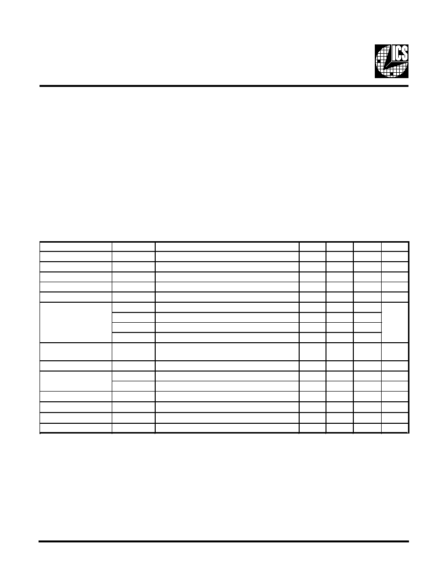
Absolute Maximum Ratings
Supply Voltage . . . . . . . . . . . . . . . . . . . . . . . . . . . . 7.0 V
Logic Inputs . . . . . . . . . . . . . . . . . . . . . . . . . . . . . . GND ≠0.5 V to V
DD
+0.5 V
Ambient Operating Temperature . . . . . . . . . . . . . -40∞C to +85∞C
Storage Temperature . . . . . . . . . . . . . . . . . . . . . . . ≠65∞C to +150∞C
Stresses above those listed under Absolute Maximum Ratings may cause permanent damage to the device. These ratings are
stress specifications only and functional operation of the device at these or any other conditions above those listed in the
operational sections of the specifications is not implied. Exposure to absolute maximum rating conditions for extended
periods may affect product reliability.
Electrical Characteristics - Input/Supply/Common Output Parameters
T
A
= 0 - 70∫ C; Supply Voltage V
D D
= 3.3 V +/-5% (unles s otherwis e s tated)
PARAM ETER
SYM BOL
CONDITIONS
M IN
TYP
M AX
UNITS
Input High Voltage
V
IH
2
V
DD
+0.3
V
Input Low Voltage
V
IL
V
SS
-0.3
0.8
V
Input High Current
I
IH
V
IN
= V
DD
0.1
5
µ
A
Input Low Current
I
IL1
V
IN
= 0 V; Inputs with no pull-up resistors
-5
2.0
µ
A
Input Low Current
I
IL2
V
IN
= 0 V; Inputs with pull-up resistors
-200
-100
µ
A
I
DD3.3 OP6 6
Select @ 66M Hz; M ax discrete cap loads
134
175
Operating
I
DD3.3 OP8 3
Select @ 83M Hz; M ax discrete cap loads
165
200
Supply Current
I
DD3 .3OP1 0 0
Select @ 100M Hz; M ax discrete cap loads
198
225
I
DD3 .3OP1 3 3
Select @ 133M Hz; M ax discrete cap loads
254
300
Power Down
Supply Current
Input frequency
F
i
V
DD
= 3.3 V
12
14.318
16
M Hz
C
IN
Logic Inputs
5
pF
C
INX
X1 & X2 pins
13.5
18
22.5
pF
Transition Time
1
T
Tran s
To 1st crossing of target Freq.
3
ms
Settling Time
1
T
S
From 1st crossing to 1% target Freq.
1
ms
Clk Stabilization
1
T
STAB
From V
DD
= 3.3 V to 1% target Freq.
3
ms
Skew
1
t
CP U -P CI
V
T
= 1.5 V
190
500
ps
Input Capacitance
1
mA
PD# = 0
I
D D 3 .3 P D
313
400
µ
A

5
ICS9342
Third party brands and names are the property of their respective owners.
Electrical Characteristics - PCI
T
A
= 0 - 70∫ C; V
DD
= 3.3 V +/-5%; C
L
=30 pF
PARAMETER
SYMBOL
CONDITIONS
MIN
TYP
MAX
UNITS
Output Impedance
R
DSP1
1
V
O
= V
DD
*(0.5)
12
21
55
Output Impedance
R
DSN1
1
V
O
= V
DD
*(0.5)
12
21.2
55
Output High Voltage
V
OH1
I
OH
= -11 mA
2.4
Output Low Voltage
V
OL1
I
OL
= 9.4 mA
0.17
0.4
V
Output High Current
I
OH1
V
OH
= 2.0 V
-60
-22
mA
Output Low Current
I
OL1
V
OL
= 0.8 V
25
47
mA
Rise Time
1
t
r1
V
OL
= 0.4 V, V
OH
= 2.4 V
0.5
1
2
ns
Fall Time
1
t
f1
V
OH
= 2.4 V, V
OL
= 0.4 V
0.5
0.9
2
ns
Duty Cycle
1
d
t1
V
T
= 1.5 V
45
50
55
%
Jitter, Cycle-to-cycle
1
t
jcyc-cyc1
V
T
= 1.5 V
170
500
ps
1
Guaranteed by design, not 100% tested in production.
Electrical Characteristics - CPU
T
A
= 0 - 70∫ C; V
DD
= 3.3 V +/-5%; C
L
= 20 pF (unless otherwise stated)
PARAM ETER
SYM BOL
CONDITIONS
M IN
TYP
M AX
UNITS
Output Impedance
R
D SP 2 B
1
V
O
= V
D D
*(0.5)
13.5
20
45
Output Impedance
R
D SN 2 B
1
V
O
= V
D D
*(0.5)
13.5
29
45
Output High Voltage
V
OH2 B
I
OH
= -8.0 mA
2
2.4
V
Output Low Voltage
V
OL2 B
I
OL
= 12 mA
0.32
0.4
V
Output High Current
I
OH2 B
V
OH
=1.7 V
-37
-16
mA
Output Low C urrent
I
OL2B
V
OL
= 0.7 V
19
26
mA
Rise Time
t
r2 B
1
V
OL
= 0.4 V, V
OH
= 2.4 V
1.13
2
ns
Fall Time
t
f2 B
1
V
OH
= 2.4 V, V
OL
= 0.4 V
1.27
2
ns
VT = 1.5 V; Cpu@ 66M , 83M , 100M
45
52
56
VT = 1.5 V; Cpu@133M & 146.6M
51
56
60
Skew
t
sk 2 B
1
VT = 1.5 V
187
200
ps
VT = 1.5 V; Normal
95
150
VT = 1.5 V; Spread, CPU = 91.58M Hz
143
200
VT = 1.5 V; Spread, CPU remaining freq.
143
175
1
Guaranteed by design, not 100% tested in production.
Duty Cy cle
d
t2 B
1
%
Jitter, Cycle-to-cycle
tj
cy c-cyc2 B
1
ps
6
ICS9342
Third party brands and names are the property of their respective owners.
Electrical Characteristics - REF, OUT , OUT /2
T
A
= 0 - 70∫ C; V
DD
= 3.3 V +/-5%; C
L
= 20 pF (unless otherwise stated)
SYM BOL
CONDITIONS
M IN
TYP
M A X
UNITS
R
D SP 5
1
V
O
= V
D D
*(0.5)
20
34
60
R
D SN 5
1
V
O
= V
D D
*(0.5)
20
31
60
V
O H 5
I
O H
= -12 mA
2.4
2.9
V
V
O L 5
I
O L
= 10 mA
0.33
0.4
V
I
O H 5
V
O H
= 2.0 V
-30
-20
mA
I
O L 5
V
O L
= 0.8 V
16
23
mA
Ris e Time
1
t
r5
V
O L
= 0.4 V, V
O H
= 2.4 V; OUT
1.5
1.8
4
ns
Fall Time
1
t
f5
V
O H
= 2.4 V, V
O L
= 0.4 V; OUT
1.5
2
4
ns
Duty Cycle
1
d
t5
V
T
= 1.5 V; OUT
45
52
55
%
Ris e Time
1
t
r5
V
O L
= 0.4 V, V
O H
= 2.4 V; OUT/2
1.5
2.2
4
ns
Fall Time
1
t
f5
V
O H
= 2.4 V, V
O L
= 0.4 V; OUT/2
1.5
2.1
4
ns
Duty Cycle
1
d
t5
V
T
= 1.5 V; OUT/2
45
50
55
%
Ris e Time
1
t
r5
V
O L
= 0.4 V, V
O H
= 2.4 V; REF
1.5
2.7
4
ns
Fall Time
1
t
f5
V
O H
= 2.4 V, V
O L
= 0.4 V; REF
1.5
2.8
4
ns
Duty Cycle
1
d
t5
V
T
= 1.5 V; REF
45
50
55
%
t
jcy c-cy c5
V
T
= 1.5 V; OUT, OUT/2
280
500
ps
t
jcy c-cy c5
V
T
= 1.5 V; R EF
450
1000
ps
1
Guaranteed b y des ign, no t 100% tes ted in production.
Jitter, Cycle-to-cycle1
Jitter, Cycle-to-cycle
1
PA RA M ETER
Output Lo w Voltage
Output High Current
Output High Voltage
Output Impedance
REF
OUT
OUT/2
Output Low Current

7
ICS9342
Third party brands and names are the property of their respective owners.
Fig. 1
Shared Pin Operation -
Input/Output Pins
The I/O pins designated by (input/output) on the ICS9342
serve as dual signal functions to the device. During initial
power-up, they act as input pins. The logic level (voltage)
that is present on these pins at this time is read and stored
into a 5-bit internal data latch. At the end of Power-On reset,
(see AC characteristics for timing values), the device changes
the mode of operations for these pins to an output function.
In this mode the pins produce the specified buffered clocks
to external loads.
To program (load) the internal configuration register for
these pins, a resistor is connected to either the VDD (logic 1)
power supply or the GND (logic 0) voltage potential. A 10
Kilohm (10K) resistor is used to provide both the solid
CMOS programming voltage needed during the power-up
programming period and to provide an insignificant load on
the output clock during the subsequent operating period.
Via to
VDD
Clock trace to load
Series Term. Res.
Programming
Header
Via to Gnd
Device
Pad
2K
W
8.2K
W
Figure 1 shows a means of implementing this function
when a switch or 2 pin header is used. With no jumper is
installed the pin will be pulled high. With the jumper in
place the pin will be pulled low. If programmability is not
necessary, than only a single resistor is necessary. The
programming resistors should be located close to the series
termination resistor to minimize the current loop area. It is
more important to locate the series termination resistor
close to the driver than the programming resistor.

8
ICS9342
Third party brands and names are the property of their respective owners.
#
D
P
#
P
F
D
P
2
V
I
D
_
T
U
O
,
1
T
U
O
F
E
R
,
I
C
P
,
U
P
C
1
1
G
N
I
N
N
U
R
G
N
I
N
N
U
R
1
0
D
E
P
P
O
T
S
G
N
I
N
N
U
R
0
1
D
E
P
P
O
T
S
D
E
P
P
O
T
S
0
0
D
E
P
P
O
T
S
D
E
P
P
O
T
S
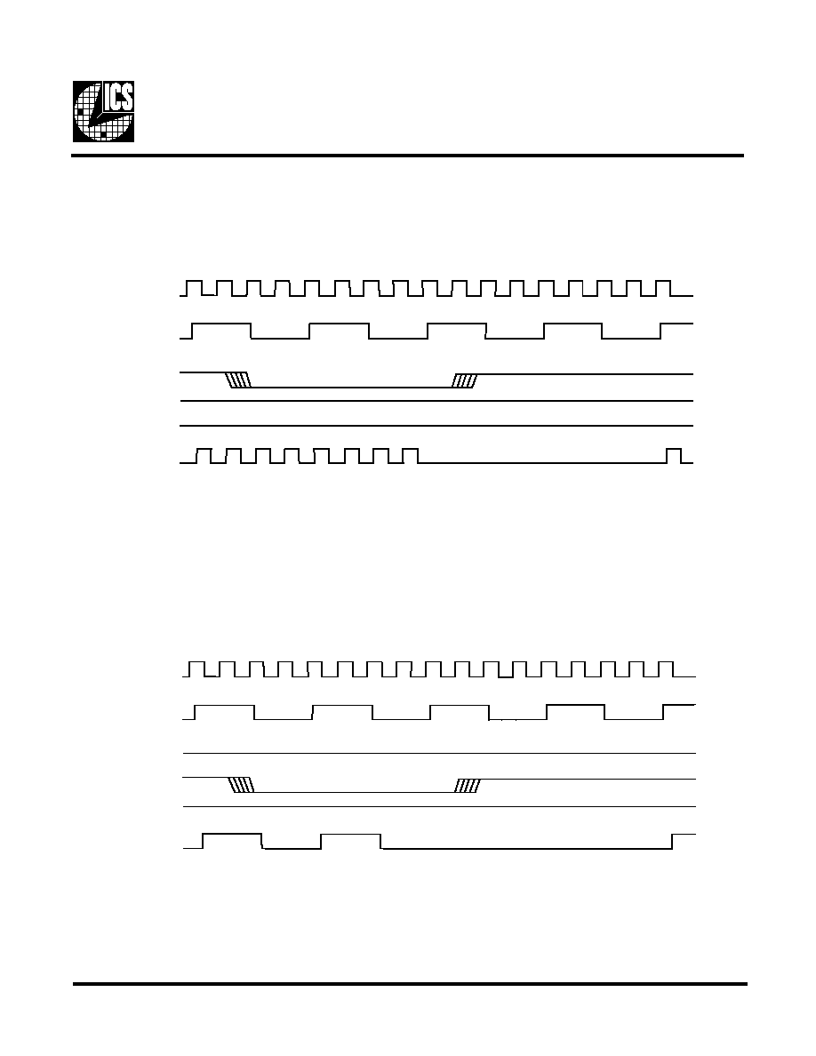
Power Management
PD# Timing Diagram
The power down selection is used to put the part into a very low power state without turning off the power to the part. PD# is
an asynchronous active low input. This signal needs to be synchronized internal to the device prior to powering down the
clock synthesizer.
Internal clocks are not running after the device is put in power down. When PD# is active low all clocks need to be driven to
a low value and held prior to turning off the VCOs and crystal. The power up latency needs to be less than 3 mS. The power
down latency should be as short as possible but conforming to the sequence requirements shown below. The REF and OUT
clocks are expected to be stopped in the LOW state as soon as possible. Due to the state of the internal logic, stopping and
holding the REF clock outputs in the LOW state may require more than one clock cycle to complete.
Notes:
1. All timing is referenced to the Internal CPU (defined as inside the ICS9342 device).
2. As shown, the outputs Stop Low on the next falling edge after PD# goes low.
3. PD# is an asynchronous input and metastable conditions may exist. This signal is synchronized inside this part.
4. The shaded sections on the VCO and the Crystal signals indicate an active clock.
5. Diagrams shown with respect to 133MHz. Similar operation when CPU is 100MHz.
CPU
PCIREF
VCO
Crystal
PD#
9
ICS9342
Third party brands and names are the property of their respective owners.
PCI_STOP# Timing Diagram
PCI_STOP# is an input to the clock synthesizer. It is used to turn off the PCIREF clock for low power operation. PCIREF clock
is required to be stopped in a low state and started such that a full high pulse width is guaranteed.
Notes:
1. All timing is referenced to CPUCLK.
2. Internal means inside the chip.
3. All other clocks continue to run undisturbed.
4. PD# and CPU_STOP# are shown in a high state.
CPUCLK
(internal)
(internal)
(externall)
PCICLK
PCI_STOP#
CPU_STOP#
PD#
PCIREF
CPU_STOP# Timing Diagram
CPU_STOP# is an asynchronous input to the clock synthesizer. It is used to turn off the CPU clocks for low power operation.
CPU_STOP# is asserted asynchronously by the external clock control logic with the rising edge of free running PCI clock
(and hence CPU clock) and must be internally synchronized to the external output. All other clocks will continue to run while
the CPU clocks are disabled. The CPU clocks must always be stopped in a low state and started in such a manner as to
guarantee that the high pulse width is a full pulse.
Notes:
1. All timing is referenced to the internal CPUCLK.
2. The internal label means inside the chip and is a reference only. This in fact may not be the way that the control is designed.
3. PD# and PCI_STOP# are shown in a high state.
CPUCLK
(internal)
(internal)
(externall)
PCICLK
PCI_STOP#
CPU_STOP#
PD#
CPUCLK
10
ICS9342
Third party brands and names are the property of their respective owners.
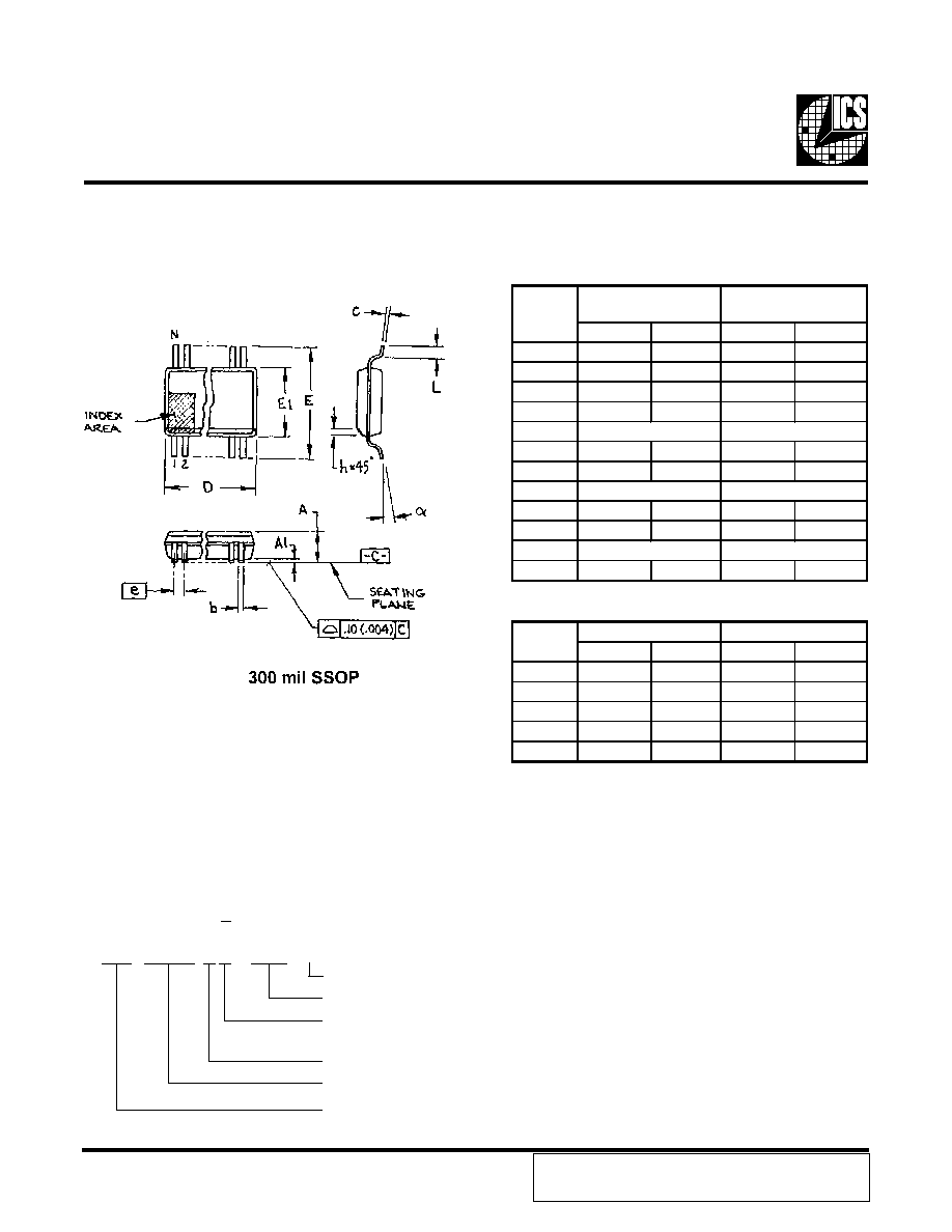
Ordering Information
ICS9342yF-T
Designation for tape and reel packaging
Pattern Number (2 or 3 digit number for parts with ROM code patterns)
Package Type
F=SSOP
Revision Designator (will not correlate with datasheet revision)
Device Type (consists of 3 or 4 digit numbers)
Prefix
ICS, AV = Standard Device
Example:
ICS XXXX y F - PPP - T
MIN
MAX
MIN
MAX
A
2.413
2.794
.095
.110
A1
0.203
0.406
.008
.016
b
0.203
0.343
.008
.0135
c
0.127
0.254
.005
.010
D
E
10.033
10.668
.395
.420
E1
7.391
7.595
.291
.299
e
0.635 BASIC
0.025 BASIC
h
0.381
0.635
.015
.025
L
0.508
1.016
.020
.040
N
0∞
8∞
0∞
8∞
VARIATIONS
MIN
MAX
MIN
MAX
28
9.398
9.652
.370
.380
34
11.303
11.557
.445
.455
48
15.748
16.002
.620
.630
56
18.288
18.542
.720
.730
64
20.828
21.082
.820
.830
SYMBOL
SEE VARIATIONS
SEE VARIATIONS
In Millimeters
COMMON DIMENSIONS
In Inches
COMMON DIMENSIONS
SEE VARIATIONS
N
D mm.
D (inch)
SEE VARIATIONS
ICS reserves the right to make changes in the device data identified in
this publication without further notice. ICS advises its customers to
obtain the latest version of all device data to verify that any
information being relied upon by the customer is current and accurate.