Integrated
Circuit
Systems, Inc.
ICS93712
Advance Information
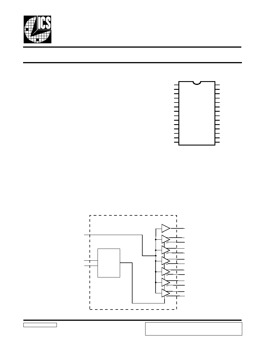
Block Diagram
2 DIMM DDR Fanout Buffer
93712 Rev - 9/08/00
Pin Configuration
28-Pin SSOP
Recommended Application:
DDR fan out buffer for VIA PRO 266 DDR chipset
Product Description/Features:
Low skew, fanout buffer
1 to 6 differential clock distribution
I
2
C for functional and output control
Feedback pin for input to output synchronization
Supports up to 2 DDR DIMMs
Frequency support for up to 400MHz DDR, SDRAMs
CMOS level control signal input
Switching Characteristics:
OUTPUT - OUTPUT skew: <100ps
Output Rise and Fall Time for DDR outputs: 650ps - 950ps
DUTY CYCLE: 47% - 53%
Pulse Skew: <100ps
ADVANCE INFORMATION documents contain information on products
in the formative or design phase development. Characteristic data and
other specifications are design goals. ICS reserves the right to change or
discontinue these products without notice.
SCLK
SDATA
BUF_IN
Control
Logic
FB_OUT
DDRT0
DDRT1
DDRT1
DDRT3
DDRT4
DDRT5
DDRC0
DDRC1
DDRC2
DDRC3
DDRC4
DDRC5
FBOUT
GND
DDRT0
DDRC0
VDD2.5
GND
DDRT1
DDRC1
VDD2.5
BUF_IN
GND
DDRT2
DDRC2
VDD2.5
GND
DDRT5
DDRC5
VDD2.5
GND
DDRT4
DDRC4
VDD2.5
GND
DDRT3
DDRC3
VDD2.5
SCLK
SDATA
ICS93712
1
2
3
4
5
6
7
8
9
10
11
12
13
14
28
27
26
25
24
23
22
21
20
19
18
17
16
15
2
ICS93712
Advance Information
Pin Descriptions
R
E
B
M
U
N
N
I
P
E
M
A
N
N
I
P
E
P
Y
T
N
O
I
T
P
I
R
C
S
E
D
1
T
U
O
_
B
F
T
U
O
k
c
a
b
d
e
e
f
l
a
n
r
e
t
x
e
r
o
f
d
e
t
a
c
i
d
e
d
,
t
u
p
t
u
o
k
c
a
b
d
e
e
F
5
2
,
1
2
,
7
1
,
4
1
,
9
,
5
5
.
2
D
D
V
R
W
P
y
l
p
p
u
s
e
g
a
t
l
o
v
V
5
.
2
8
2
,
4
2
,
0
2
,
1
1
,
6
,
2
D
N
G
R
W
P
d
n
u
o
r
G
3
,
7
,
2
1
,
9
1
,
3
2
,
7
2
T
R
D
D
)
0
:
5
(
T
U
O
.
s
t
u
p
t
u
o
r
i
a
p
l
a
i
t
n
e
r
e
f
f
i
d
f
o
k
c
o
l
C
"
e
u
r
T
"
4
,
8
,
3
1
,
8
1
,
2
2
,
6
2
)
0
:
5
(
C
R
D
D
T
U
O
.
s
t
u
p
t
u
o
r
i
a
p
l
a
i
t
n
e
r
e
f
f
i
d
f
o
s
k
c
o
l
c
"
y
r
o
t
n
e
m
e
l
p
m
o
C
"
0
1
N
I
_
F
U
B
N
I
t
u
p
n
i
r
e
f
f
u
b
d
e
d
n
e
e
l
g
n
i
S
5
1
A
T
A
D
S
O
/
I
I
r
o
f
n
i
p
a
t
a
D
2
t
n
a
r
e
l
o
t
V
5
y
r
t
i
u
c
r
i
c
C
6
1
K
L
C
S
N
I
I
f
o
t
u
p
n
i
k
c
o
l
C
2
t
u
p
n
i
t
n
a
r
e
l
o
t
V
5
,
t
u
p
n
i
C
Byte 1: Reserved Register
(1= enable, 0 = disable)
T
I
B
#
N
I
P
D
W
P
N
O
I
T
P
I
R
C
S
E
D
7
t
i
B
-
1
d
e
v
r
e
s
e
R
6
t
i
B
-
1
d
e
v
r
e
s
e
R
5
t
i
B
-
1
d
e
v
r
e
s
e
R
4
t
i
B
-
1
d
e
v
r
e
s
e
R
3
t
i
B
-
1
d
e
v
r
e
s
e
R
2
t
i
B
-
1
d
e
v
r
e
s
e
R
1
t
i
B
-
1
d
e
v
r
e
s
e
R
0
t
i
B
-
1
d
e
v
r
e
s
e
R
Byte 2: Reserved Register
(1= enable, 0 = disable)
T
I
B
#
N
I
P
D
W
P
N
O
I
T
P
I
R
C
S
E
D
7
t
i
B
-
1
d
e
v
r
e
s
e
R
6
t
i
B
-
1
d
e
v
r
e
s
e
R
5
t
i
B
-
1
d
e
v
r
e
s
e
R
4
t
i
B
-
1
d
e
v
r
e
s
e
R
3
t
i
B
-
1
d
e
v
r
e
s
e
R
2
t
i
B
-
1
d
e
v
r
e
s
e
R
1
t
i
B
-
1
d
e
v
r
e
s
e
R
0
t
i
B
-
1
d
e
v
r
e
s
e
R
Byte 4: Reserved Register
(1= enable, 0 = disable)
Byte 3: Reserved Register
(1= enable, 0 = disable)
T
I
B
#
N
I
P
D
W
P
N
O
I
T
P
I
R
C
S
E
D
7
t
i
B
-
1
d
e
v
r
e
s
e
R
6
t
i
B
-
1
d
e
v
r
e
s
e
R
5
t
i
B
-
1
d
e
v
r
e
s
e
R
4
t
i
B
-
1
d
e
v
r
e
s
e
R
3
t
i
B
-
1
d
e
v
r
e
s
e
R
2
t
i
B
-
1
d
e
v
r
e
s
e
R
1
t
i
B
-
1
d
e
v
r
e
s
e
R
0
t
i
B
-
1
d
e
v
r
e
s
e
R
T
I
B
#
N
I
P
D
W
P
N
O
I
T
P
I
R
C
S
E
D
7
t
i
B
-
1
d
e
v
r
e
s
e
R
6
t
i
B
-
1
d
e
v
r
e
s
e
R
5
t
i
B
-
1
d
e
v
r
e
s
e
R
4
t
i
B
-
1
d
e
v
r
e
s
e
R
3
t
i
B
-
1
d
e
v
r
e
s
e
R
2
t
i
B
-
1
d
e
v
r
e
s
e
R
1
t
i
B
-
1
d
e
v
r
e
s
e
R
0
t
i
B
-
1
d
e
v
r
e
s
e
R
3
ICS93712
Advance Information
Byte 6: Output Control
(1= enable, 0 = disable)
Byte 7: Output Control
(1= enable, 0 = disable)
T
I
B
#
N
I
P
D
W
P
N
O
I
T
P
I
R
C
S
E
D
7
t
i
B
-
1
)
d
e
v
r
e
s
e
R
(
6
t
i
B
-
0
)
d
e
v
r
e
s
e
R
(
5
t
i
B
-
0
)
d
e
v
r
e
s
e
R
(
4
t
i
B
-
0
)
d
e
v
r
e
s
e
R
(
3
t
i
B
-
1
*
)
d
e
v
r
e
s
e
R
(
2
t
i
B
6
2
,
7
2
1
5
C
R
D
D
,
5
T
R
D
D
1
t
i
B
2
2
,
3
2
1
4
C
R
D
D
,
4
T
R
D
D
0
t
i
B
8
1
,
9
1
1
3
C
R
D
D
,
3
T
R
D
D
T
I
B
#
N
I
P
D
W
P
N
O
I
T
P
I
R
C
S
E
D
7
t
i
B
-
1
*
d
e
v
r
e
s
e
R
6
t
i
B
-
1
*
d
e
v
r
e
s
e
R
5
t
i
B
-
1
*
d
e
v
r
e
s
e
R
4
t
i
B
3
1
,
2
1
1
2
T
R
D
D
2
C
R
D
D
3
t
i
B
-
1
*
d
e
v
r
e
s
e
R
2
t
i
B
8
,
7
1
1
T
R
D
D
1
C
R
D
D
1
t
i
B
-
1
*
d
e
v
r
e
s
e
R
0
t
i
B
4
,
3
1
0
C
R
D
D
,
0
T
R
D
D
Note:
* For lower power consumption, these bits should be driven to 0.
T
I
B
#
N
I
P
D
W
P
N
O
I
T
P
I
R
C
S
E
D
7
t
i
B
-
1
d
e
v
r
e
s
e
R
6
t
i
B
-
1
d
e
v
r
e
s
e
R
5
t
i
B
-
1
d
e
v
r
e
s
e
R
4
t
i
B
-
1
d
e
v
r
e
s
e
R
3
t
i
B
-
1
d
e
v
r
e
s
e
R
2
t
i
B
-
1
d
e
v
r
e
s
e
R
1
t
i
B
-
1
d
e
v
r
e
s
e
R
0
t
i
B
-
1
d
e
v
r
e
s
e
R
Byte 5: Reserved Register
(1= enable, 0 = disable)
Notes:
1. Refers to transition on noninverting output.
2. While the pulse skew is almost constant over frequency, the duty cycle error increases at
higher frequencies. This is due to the formula: duty cycle=t
wH
/t
c
, were the cycle (t
c
)
decreases as the frequency goes up.
Switching Characteristics
PARAMETER
SYMBOL
CONDITION
MIN
TYP
MAX
UNITS
Maximum Operating Frequency
66
200
MHz
Input clock duty cycle
d
tin
40
60
%
Output to Output Skew
T
skew
100
ps
Pulse skew
T
skewp
100
ps
66MHz to 100MHz
48
52
%
101MHz to 167MHz
47
53
%
Rise Time, Fall Time
tr, tf
Load = 120
/16pF
650
950
ps
Duty cycle
D
C
2
4
ICS93712
Advance Information
Absolute Maximum Ratings
Supply Voltage (VDD) . . . . . . . . . . . . . . . . . . . . . -0.5V to 3.6V
Logic Inputs . . . . . . . . . . . . . . . . . . . . . . . . . . . . GND 0.5 V to V
DD
+0.5 V
Ambient Operating Temperature . . . . . . . . . . . . 0∞C to +85∞C
Storage Temperature . . . . . . . . . . . . . . . . . . . . . . 65∞C to +150∞C
Stresses above those listed under Absolute Maximum Ratings may cause permanent damage to the device. These ratings are
stress specifications only and functional operation of the device at these or any other conditions above those listed in the
operational sections of the specifications is not implied. Exposure to absolute maximum rating conditions for extended periods
may affect product reliability.
Ele ctrical Characte ristics - Input/Supply /Com m on Output Param e te rs
T
A
= 0 - 85C; Supply Voltage VDD = 2.5 V +/- 0.2V (unless otherwise stated)
PARAM ETER
SYM B OL
CONDITIONS
M IN
TYP
M AX
UNITS
Input High C urrent
I
IH
VI = VDD or GND
µA
Input Low Current
I
IL
VI = VDD or GND
µA
I
DD2 .5
CL = 0pf
mA
I
DDPD
CL = 0pf
100
µ
A
Output High Current
I
OH
VDD = 2.3V, V
OUT
= 1V
-18
mA
Output Low Current
I
OL
VDD = 2.3V, V
OUT
= 1.2V
26
mA
VDD = min to max,
IOH = -1 mA
V
VDD = 2.3V,
IOH = -12 mA
V
VDD = min to max
I
OL
=1 mA
0.1
VDD = 2.3V
IOH=12 mA
0.6
V
Input Capacitance
1
C
IN
VI = GND or VDD
2
pF
1
Guaranteed by design, not 100% tested in production.
Operating Supply Current
High-level output
voltage
V
OH
Low-level output voltage
V
OL
Re com m e nde d Ope rating Condition
T
A
= 0 - 85C; Supply Vo ltage AVDD, VDD = 2.5 V +/- 0.2V (unless otherwise stated)
PARAM ETER
SYM BOL
CONDITIONS
M IN
TYP
M AX
UNITS
Power Supp ly Voltage
V
DD
2.3
2.5
2.7
V
Input High Voltage
V
IH
OE input
V
Input Low Voltage
V
IL
OE input
V
Input voltage level
V
IN
V
Output differential-pair
crossing voltage
V
OC
V
1
Guaranteed by design, not 100% tested in production.

5
ICS93712
Advance Information
1.
The ICS clock generator is a slave/receiver, I
2
C component. It can read back the data stored in the latches for verification.
Read-Back will support Intel PIIX4 "Block-Read" protocol.
2.
The data transfer rate supported by this clock generator is 100K bits/sec or less (standard mode)
3.
The input is operating at 3.3V logic levels.
4.
The data byte format is 8 bit bytes.
5.
To simplify the clock generator I
2
C interface, the protocol is set to use only "Block-Writes" from the controller. The
bytes must be accessed in sequential order from lowest to highest byte with the ability to stop after any complete byte
has been transferred. The Command code and Byte count shown above must be sent, but the data is ignored for those
two bytes. The data is loaded until a Stop sequence is issued.
6.
At power-on, all registers are set to a default condition, as shown.
Controlle r (Host)
ICS (Sla ve /Re ce ive r)
Start Bit
Address
D2
(H )
A CK
Dumm y Comm and Code
A CK
Dumm y Byte Count
A CK
Byte 0
A CK
Byte 1
A CK
Byte 2
A CK
Byte 3
A CK
Byte 4
A CK
Byte 5
A CK
Byte 6
A CK
Byte 7
A CK
Stop Bit
How to Write:
Controlle r (Host)
ICS (Sla ve /Re ce ive r)
Start Bit
A ddress
D3
(H )
A CK
Byte Count
ACK
Byte 0
ACK
Byte 1
ACK
Byte 2
ACK
Byte 3
ACK
Byte 4
ACK
Byte 5
ACK
Byte 6
ACK
Byte 7
Stop Bit
How to Read:
General I
2
C serial interface information
The information in this section assumes familiarity with I
2
C programming.
For more information, contact ICS for an I
2
C programming application note.
How to Write:
Controller (host) sends a start bit.
Controller (host) sends the write address D2
(H)
ICS clock will acknowledge
Controller (host) sends a dummy command code
ICS clock will acknowledge
Controller (host) sends a dummy byte count
ICS clock will acknowledge
Controller (host) starts sending first byte (Byte 0)
through byte 6
ICS clock will acknowledge each byte one at a time.
Controller (host) sends a Stop bit
How to Read:
Controller (host) will send start bit.
Controller (host) sends the read address D3
(H)
ICS clock will acknowledge
ICS clock will send the byte count
Controller (host) acknowledges
ICS clock sends first byte (Byte 0) through byte 7
Controller (host) will need to acknowledge each byte
Controller (host) will send a stop bit
Notes:
6
ICS93712
Advance Information
Ordering Information
ICS93712yF-T
Designation for tape and reel packaging
Pattern Number (2 or 3 digit number for parts with ROM code patterns)
Package Type
F=SSOP
Revision Designator (will not correlate with datasheet revision)
Device Type (consists of 3 or 4 digit numbers)
Prefix
ICS, AV = Standard Device
Example:
ICS XXXX y F - PPP - T
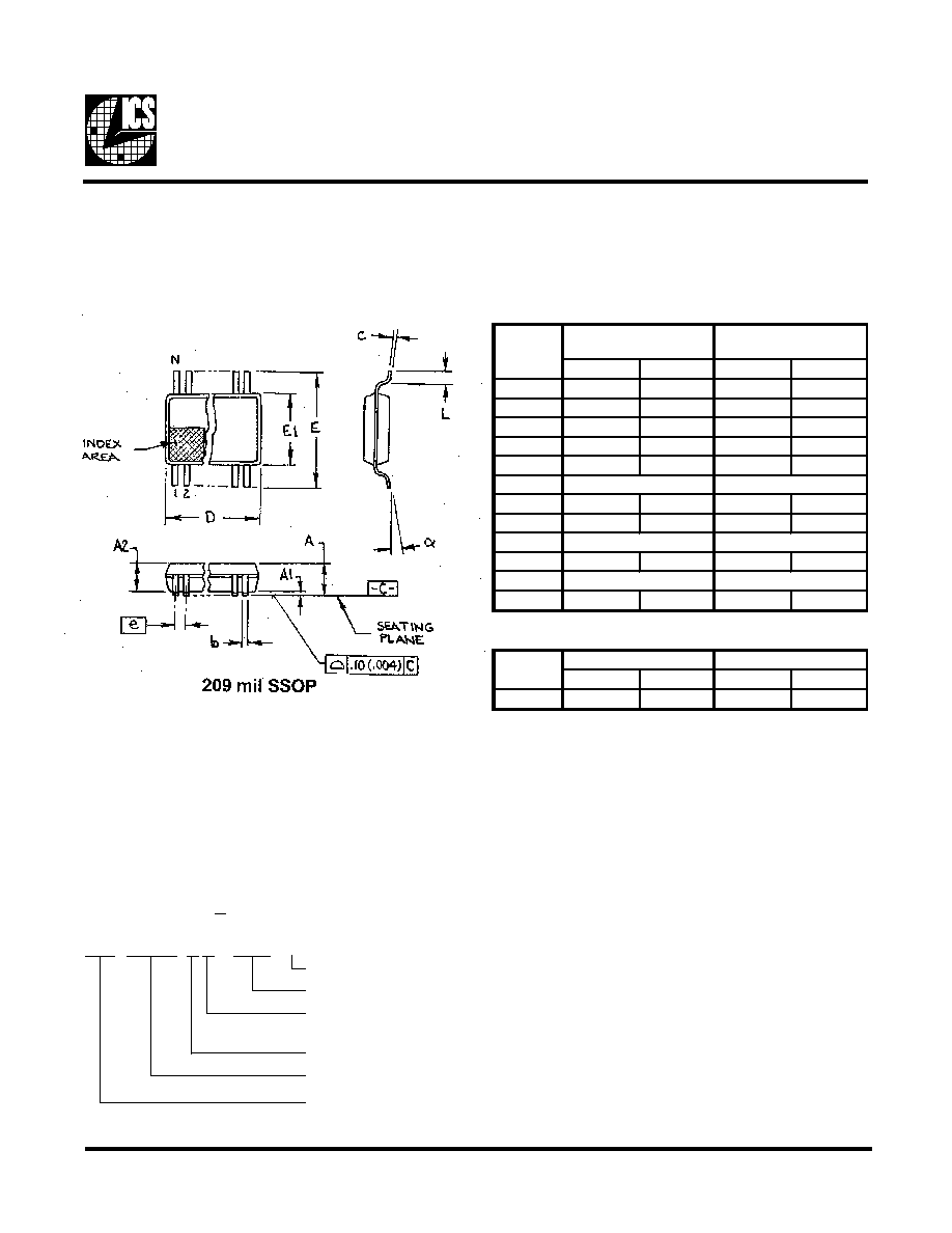
MIN
MAX
MIN
MAX
A
-
2.00
-
.079
A1
0.05
-
.002
-
A2
1.65
1.85
.065
.073
b
0.22
0.38
.009
.015
c
0.09
0.25
.0035
.010
D
E
7.40
8.20
.291
.323
E1
5.00
5.60
.197
.220
e
L
0.55
0.95
.022
.037
N
0∞
8∞
0∞
8∞
VARIATIONS
MIN
MAX
MIN
MAX
28
9.90
10.50
.390
.413
MO-150 JEDEC
Doc.# 10-0033
6/1/00 Rev B
SYMBOL
SEE VARIATIONS
SEE VARIATIONS
In Millimeters
COMMON DIMENSIONS
In Inches
COMMON DIMENSIONS
SEE VARIATIONS
0.65 BASIC
0.0256 BASIC
N
D mm.
D (inch)
SEE VARIATIONS