Integrated
Circuit
Systems, Inc.
ICS93722
0539D--12/09/02
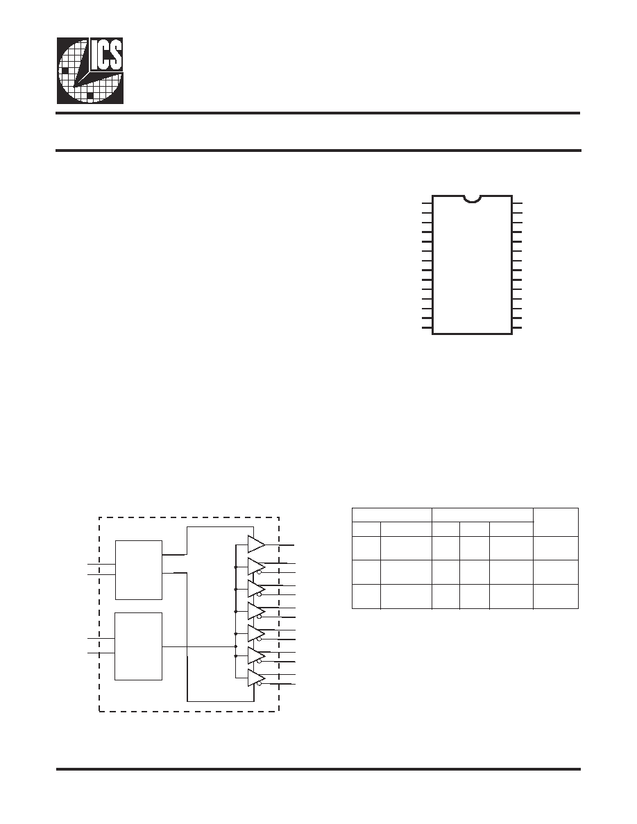
Block Diagram
Low Cost DDR Phase Lock Loop Zero Delay Buffer
Pin Configuration
28-Pin SSOP
Recommended Application:
DDR Zero Delay Clock Buffer
Product Description/Features:
∑
Low skew, low jitter PLL clock driver
∑
I
2
C for functional and output control
∑
Feedback pins for input to output synchronization
∑
Spread Spectrum tolerant inputs
∑
3.3V tolerant CLK_INT input
Switching Characteristics:
∑
PEAK - PEAK jitter (66MHz): <120ps
∑
PEAK - PEAK jitter (>100MHz): <75ps
∑
CYCLE - CYCLE jitter (66MHz):<110ps
∑
CYCLE - CYCLE jitter (>100MHz):<65ps
∑
OUTPUT - OUTPUT skew: <100ps
∑
Output Rise and Fall Time: 650ps - 950ps
∑
DUTY CYCLE: 49.5% - 50.5%
Functionality
FB_INT
CLK_INT
CLK_INT
SCLK
SCLK
SDATA
Control
Control
Logic
FB_OUTT
CLKT0
CLKT1
CLKT2
CLKT3
CLKT4
CLKT5
CLKC0
CLKC1
CLKC2
CLKC3
CLKC4
CLKC5
PLL
S
T
U
P
N
I
S
T
U
P
T
U
O
e
t
a
t
S
L
L
P
D
D
V
A
T
N
I
_
K
L
C
T
K
L
C
C
K
L
C
T
T
U
O
_
B
F
V
5
.
2
)
m
o
n
(
L
L
H
L
n
o
V
5
.
2
)
m
o
n
(
H
H
L
H
n
o
V
5
.
2
)
m
o
n
(
z
H
M
0
2
<
Z
Z
Z
f
f
o
CLKC0
CLKT0
VDD
CLKT1
CLKC1
GND
SCLK
CLK_INT
N/C
VDDA
GND
VDD
CLKT2
CLKC2
GND
CLKC5
CLKT5
CLKC4
CLKT4
VDD
SDATA
N/C
FB_INT
FB_OUTT
N/C
CLKT3
CLKC3
GND
ICS937
22
1
2
3
4
5
6
7
8
9
10
11
12
13
14
28
27
26
25
24
23
22
21
20
19
18
17
16
15
2
ICS9372 2
0539D--12/09/02
Pin Descriptions
R
E
B
M
U
N
N
I
P
E
M
A
N
N
I
P
E
P
Y
T
N
O
I
T
P
I
R
C
S
E
D
8
2
,
5
1
,
1
1
,
6
D
N
G
R
W
P
d
n
u
o
r
G
1
,
5
,
4
1
,
6
1
,
5
2
,
7
2
)
0
:
5
(
C
K
L
C
T
U
O
.
s
t
u
p
t
u
o
r
i
a
p
l
a
i
t
n
e
r
e
f
f
i
d
f
o
s
k
c
o
l
c
"
y
r
a
t
n
e
m
e
l
p
m
o
C
"
2
,
4
,
3
1
,
7
1
,
4
2
,
6
2
)
0
:
5
(
T
K
L
C
T
U
O
.
s
t
u
p
t
u
o
r
i
a
p
l
a
i
t
n
e
r
e
f
f
i
d
f
o
k
c
o
l
C
"
e
u
r
T
"
3
2
,
2
1
,
3
D
D
V
R
W
P
V
5
.
2
y
l
p
p
u
s
r
e
w
o
P
7
K
L
C
S
N
I
I
f
o
t
u
p
n
i
k
c
o
l
C
2
t
u
p
n
i
t
n
a
r
e
l
o
t
V
5
,
t
u
p
n
i
C
8
T
N
I
_
K
L
C
N
I
t
u
p
n
i
k
c
o
l
c
e
c
n
e
r
e
f
e
r
"
e
u
r
T
"
1
2
,
8
1
,
9
C
/
N
-
d
e
t
c
e
n
n
o
c
t
o
N
0
1
A
D
D
V
R
W
P
V
5
.
2
,
y
l
p
p
u
s
r
e
w
o
p
g
o
l
a
n
A
9
1
T
T
U
O
_
B
F
T
U
O
t
a
s
e
h
c
t
i
w
s
t
I
.
k
c
a
b
d
e
e
f
l
a
n
r
e
t
x
e
r
o
f
d
e
t
a
c
i
d
e
d
,
t
u
p
t
u
o
k
c
a
b
d
e
e
F
"
e
u
r
T
"
.
T
N
I
_
B
F
o
t
d
e
r
i
w
e
b
t
s
u
m
t
u
p
t
u
o
s
i
h
T
.
K
L
C
e
h
t
s
a
y
c
n
e
u
q
e
r
f
e
m
a
s
e
h
t
0
2
T
N
I
_
B
F
N
I
r
o
f
L
L
P
l
a
n
r
e
t
n
i
e
h
t
o
t
l
a
n
g
i
s
k
c
a
b
d
e
e
f
s
e
d
i
v
o
r
p
,
t
u
p
n
i
k
c
a
b
d
e
e
F
"
e
u
r
T
"
.
r
o
r
r
e
e
s
a
h
p
e
t
a
n
i
m
il
e
o
t
T
N
I
_
K
L
C
h
t
i
w
n
o
i
t
a
z
i
n
o
r
h
c
n
y
s
2
2
A
T
A
D
S
N
I
I
r
o
f
t
u
p
n
i
a
t
a
D
2
t
u
p
n
i
t
n
a
r
e
l
o
t
V
5
,
t
u
p
n
i
l
a
i
r
e
s
C
Byte 5: Output Control
(1= enable, 0 = disable)
Byte 6: Output Control
(1= enable, 0 = disable)
Note: PWD = Power Up Default
Bytes 0 to 4 are reserved power up default = 1.
T
I
B
#
N
I
P
D
W
P
N
O
I
T
P
I
R
C
S
E
D
7
t
i
B
1
,
2
1
)
C
&
T
(
0
K
L
C
6
t
i
B
5
,
4
1
d
e
v
r
e
s
e
R
5
t
i
B
-
1
d
e
v
r
e
s
e
R
4
t
i
B
-
1
d
e
v
r
e
s
e
R
3
t
i
B
4
1
,
3
1
1
)
C
&
T
(
2
K
L
C
2
t
i
B
6
1
,
7
1
1
)
C
&
T
(
3
K
L
C
1
t
i
B
-
1
d
e
v
r
e
s
e
R
0
t
i
B
-
1
d
e
v
r
e
s
e
R
T
I
B
#
N
I
P
D
W
P
N
O
I
T
P
I
R
C
S
E
D
7
t
i
B
-
1
d
e
v
r
e
s
e
R
6
t
i
B
-
1
d
e
v
r
e
s
e
R
5
t
i
B
-
1
d
e
v
r
e
s
e
R
4
t
i
B
-
1
d
e
v
r
e
s
e
R
3
t
i
B
,
4
2
5
2
1
)
C
&
T
(
4
K
L
C
2
t
i
B
-
1
d
e
v
r
e
s
e
R
1
t
i
B
,
6
2
7
2
1
)
C
&
T
(
5
K
L
C
0
t
i
B
-
1
d
e
v
r
e
s
e
R
3
ICS93722
0539D--12/09/02
Absolute Maximum Ratings
Supply Voltage (VDD & AVDD) . . . . . . . . . . -0.5V to 3.6V
Logic Inputs . . . . . . . . . . . . . . . . . . . . . . . . . GND ≠0.5 V to V
DD
+0.5 V
Ambient Operating Temperature . . . . . . . . . 0∞C to +85∞C
Case Temperature . . . . . . . . . . . . . . . . . . . . 115∞C
Storage Temperature . . . . . . . . . . . . . . . . . . ≠65∞C to +150∞C
Stresses above those listed under
Absolute Maximum Ratings may cause permanent damage to the device. These
ratings are stress specifications only and functional operation of the device at these or any other conditions above
those listed in the operational sections of the specifications is not implied. Exposure to absolute maximum rating
conditions for extended periods may affect product reliability.
Electrical Characteristics - Input / Supply / Common Output Parameters
T
A
= 0 - 70∞C; Supply Voltage V
DD
= 2.5 V +/-0.2V (unless otherwise stated)
PARAMETER
SYMBOL
CONDITIONS
MIN
TYP
MAX
UNITS
Input High Current
I
IH
V
IN
= V
DD
or GND
µ
A
Input Low Current
I
IL
V
IN
= V
DD
or GND
µ
A
I
DD2.5
C
L
= 0 pF at 133 MHz
275
325
mA
I
DDPD
C
L
= 0 pF
100
µ
A
Output High Current
I
OH
V
DD
= 2.3V, V
OUT
= 1V
-43
-18
mA
Output High Current
I
OL
V
DD
= 2.3V, V
OUT
= 1.2V
26
43
mA
High Impedance Output
Current
I
OZ
V
DD
= 2.7V, V
OUT
= V
DD
or GND
10
µ
A
Input Clamp Voltage
V
IK
I
IN
= -18 mA;
V
V
DD
= min to max, I
OH
= -1mA
2.1
2.42
V
V
DD
= 2.3V, I
OH
= -12mA
1.87
V
V
OL
V
DD
= min to max, I
OH
= 1mA
0.04
0.1
V
V
DD
= 2.3V, I
OH
= 12mA
0.35
0.6
V
Input Capacitance
1
C
IN
V
IN
= V
DD
or GND
pF
Output Capacitance
1
C
OUT
V
OUT
= V
DD
or GND
3
pF
1. Guaranteed by design, not 100% tested in production.
Operating Supply Current
V
OH
Low-level Output Voltage
High-level Output Voltage
4
ICS9372 2
0539D--12/09/02
Recommended Operating Conditions
T
A
= 0 - 70∞C; Supply Voltage AV
DD
, V
DD
= 2.5 V +/-0.2V (unless otherwise stated)
PARAMETER
SYMBOL
CONDITIONS
MIN
TYP
MAX
UNITS
Analog / Core Supply Voltage
V
DD
, AV
DD
2.3
2.5
2.7
V
V
IL
V
DD
/2 - 0.5V
V
V
IH
V
DD
/2 + 0.5V
V
Inpu Duty Cycle
I
DC
40
60
Input max jitter
I
TCYC
500
ps
Input Voltage Level
Timing Requirements
T
A
= 0 - 70∞C; Supply Voltage AV
DD
, V
DD
= 2.5 V +/-0.2V (unless otherwise stated)
PARAMETER
SYMBOL
CONDITIONS
MIN
TYP
MAX
UNITS
Operating Clock Frequency
1
freq
op
66
200
MHz
Input Clock Duty Cycle
1
d
tin
40
60
%
Clock Stabilization
1
t
STAB
from V
DD
= 2.5V to 1% target
frequency
100
µ
s
1. Guaranteed by design, not 100% tested in production.
Switching Characteristics
T
A
= 0 - 70∞C; Supply Voltage V
DD
= 2.5 V +/-0.2V (unless otherwise stated)
PARAMETER
SYMBOL
CONDITIONS
MIN
TYP
MAX
UNITS
66 MHz
120
100 - 200 MHz
75
66 MHz
50
110
100 - 200 MHz
25
65
Phase Error
1
t
(phase error)
CLK_INT to FB_INT
-150
50
150
ps
Output to output Skew
1
T
skew
V
T
= 50%
70
100
ps
Pulse Skew
1
T
skewp
100
ps
V
T
= 50%, 66 MHz to 100 MHz
49.5
50
50.5
V
T
= 50%, 101 MHz to 167 MHz
49
50
51
Single-ended 20 - 80 %
Load = 120
/ 12 pF
1. Guaranteed by design, not 100% tested in production.
2. Refers to transistion on non-inverting output.
3. While the pulse skew is almost constant over frequency, the duty cycle error increases at higher frequencies.
This is due to the formula: duty cycle = t
wH
/ t
C
, where the cycle time (t
C
) decreases as the frequency increases.
Duty Cycle (differential)
1,3
950
ps
%
D
C
Rise Time, Fall Time
1
t
R
, t
F
450
550
Absolute Jitter
1
T
jabs
ps
Cycle to cycle Jitter
1,2
T
cyc-cyc
ps

5
ICS93722
0539D--12/09/02
1.
The ICS clock generator is a slave/receiver, I
2
C component. It can read back the data stored in the latches for
verification. Read-Back will support Intel PIIX4 "Block-Read" protocol.
2.
The data transfer rate supported by this clock generator is 100K bits/sec or less (standard mode)
3.
The input is operating at 3.3V logic levels.
4.
The data byte format is 8 bit bytes.
5.
To simplify the clock generator I
2
C interface, the protocol is set to use only "Block-Writes" from the
controller. The bytes must be accessed in sequential order from lowest to highest byte with the ability to stop
after any complete byte has been transferred. The Command code and Byte count shown above must be
sent, but the data is ignored for those two bytes. The data is loaded until a Stop sequence is issued.
6.
At power-on, all registers are set to a default condition, as shown.
General I
2
C serial interface information
The information in this section assumes familiarity with I
2
C programming.
For more information, contact ICS for an I
2
C programming application note.
How to Write:
∑ Controller (host) sends a start bit.
∑ Controller (host) sends the write address D4
(H)
∑ ICS clock will acknowledge
∑ Controller (host) sends a dummy command code
∑ ICS clock will acknowledge
∑ Controller (host) sends a dummy byte count
∑ ICS clock will acknowledge
∑ Controller (host) starts sending first byte (Byte 0)
through byte 6
∑ ICS clock will acknowledge each byte one at a time.
∑ Controller (host) sends a Stop bit
How to Read:
∑ Controller (host) will send start bit.
∑ Controller (host) sends the read address D5
(H)
∑ ICS clock will acknowledge
∑ ICS clock will send the byte count
∑ Controller (host) acknowledges
∑ ICS clock sends first byte (Byte 0) through byte 6
∑ Controller (host) will need to acknowledge each byte
∑ Controller (host) will send a stop bit
Notes:
Controlle r (Host)
ICS (Sla ve /Re ce ive r)
Start Bit
Address
D4
(H )
A CK
Dummy Command Code
A CK
Dummy Byte Count
A CK
Byte 0
A CK
Byte 1
A CK
Byte 2
A CK
Byte 3
A CK
Byte 4
A CK
Byte 5
A CK
Byte 6
A CK
Stop Bit
How to Write:
Controlle r (Host)
ICS (Sla ve /Re ce ive r)
Start Bit
Address
D5(
H )
A CK
Byte Count
ACK
Byte 0
ACK
Byte 1
ACK
Byte 2
ACK
Byte 3
ACK
Byte 4
ACK
Byte 5
ACK
Byte 6
ACK
Stop Bit
How to Read:
6
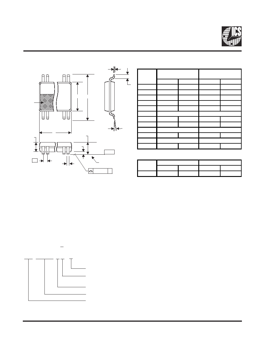
ICS9372 2
0539D--12/09/02
MIN
MAX
MIN
MAX
A
-
2.00
-
.079
A1
0.05
-
.002
-
A2
1.65
1.85
.065
.073
b
0.22
0.38
.009
.015
c
0.09
0.25
.0035
.010
D
E
7.40
8.20
.291
.323
E1
5.00
5.60
.197
.220
e
L
0.55
0.95
.022
.037
N
0∞
8∞
0∞
8∞
VARIATIONS
MIN
MAX
MIN
MAX
28
9.90
10.50
.390
.413
MO-150 JEDEC
Doc.# 10-0033
6/1/00 Rev B
SYMBOL
SEE VARIATIONS
SEE VARIATIONS
In Millimeters
COMMON DIMENSIONS
In Inches
COMMON DIMENSIONS
SEE VARIATIONS
0.65 BASIC
0.0256 BASIC
N
D mm.
D (inch)
SEE VARIATIONS
Ordering Information
ICS93722yFT
Designation for tape and reel packaging
Package Type
F = SSOP
Revision Designator (will not correlate with datasheet revision)
Device Type
Prefix
Example:
ICS XXXXX y F - T
SEATING
PLANE
SEATING
PLANE
A1
A
A2
e
- C -
- C -
b
.10 (.004) C
.10 (.004) C
c
L
INDEX
AREA
INDEX
AREA
1 2
1 2
N
D
E1
E
209 mil SSOP