DATASHEET SEARCH SITE | WWW.ALLDATASHEET.COM
Integrated
Circuit
Systems, Inc.
ICS93732
0578H--02/19/04
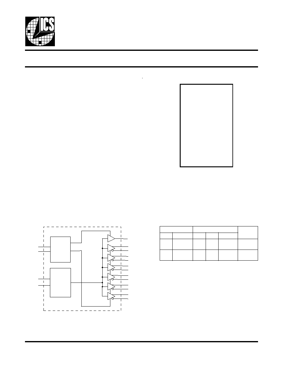
Block Diagram
Low Cost DDR Phase Lock Loop Zero Delay Buffer
Pin Configuration
Recommended Application:
DDR Zero Delay Clock Buffer
Product Description/Features:
·
Low skew, low jitter PLL clock driver
·
Max frequency supported = 266MHz (DDR 533)
·
I
2
C for functional and output control
·
Feedback pins for input to output synchronization
·
Spread Spectrum tolerant inputs
·
3.3V tolerant CLK_INT input
Switching Characteristics:
·
CYCLE - CYCLE jitter (66MHz): <120ps
·
CYCLE - CYCLE jitter (>100MHz): <65ps
·
CYCLE - CYCLE jitter (>200MHz): <75ps
·
OUTPUT - OUTPUT skew: <100ps
·
DUTY CYCLE: 49.5% - 50.5%
Functionality
S
T
U
P
N
I
S
T
U
P
T
U
O
e
t
a
t
S
L
L
P
D
D
V
A
T
N
I
_
K
L
C
T
K
L
C
C
K
L
C
T
T
U
O
_
B
F
V
5
.
2
)
m
o
n
(
L
L
H
L
n
o
V
5
.
2
)
m
o
n
(
H
H
L
H
n
o
FB_INT
FB_INT
CLK_INT
CLK_INT
SCLK
SCLK
SD
SDA
AT
TA
A
Control
Control
Logic
Logic
FB_OUTT
FB_OUTT
DDRC0
DDRC0
PLL
PLL
DDRT0
DDRT0
DDRC1
DDRC1
DDRT1
DDRT1
DDRC2
DDRC2
DDRT2
DDRT2
DDRC3
DDRC3
DDRT3
DDRT3
DDRC4
DDRC4
DDRT4
DDRT4
DDRC5
DDRC5
DDRT5
DDRT5
DDRC0
1
28 GND
DDRT0
2
27 DDRC5
VDD
3
26 DDRT5
DDRT1
4
25 DDRC4
DDRC1
5
24 DDRT4
GND
6
23 VDD
SCLK
7
22 SDATA
CLK_INT
8
21 N/C
N/C
9
20 FB_INT
VDDA 10
19 FB_OUT
GND 11
18 N/C
VDD 12
17 DDRT3
DDRT2 13
16 DDRC3
DDRC2 14
15 GND
I
C
S
9
373
2
28-Pin 209mil SSOP
28-Pin 173mil TSSOP
2
ICS93732
0578H--02/19/04
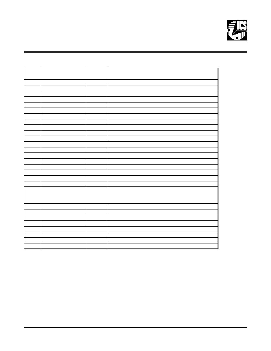
Pin Descriptions
PIN #
PIN NAME
PIN TYPE DESCRIPTION
1
DDRC0
OUT
"Complimentary" Clock of differential pair output.
2
DDRT0
OUT
"True" Clock of differential pair output.
3
VDD
PWR
Power supply, nominal 2.5V
4
DDRT1
OUT
"True" Clock of differential pair output.
5
DDRC1
OUT
"Complimentary" Clock of differential pair output.
6
GND
PWR
Ground pin.
7
SCLK
IN
Clock pin of I2C circuitry 5V tolerant
8
CLK_INT
IN
"True" reference clock input.
9
N/C
N/C
No Connection.
10
VDDA
PWR
2.5V power for the PLL core.
11
GND
PWR
Ground pin.
12
VDD
PWR
Power supply, nominal 2.5V
13
DDRT2
OUT
"True" Clock of differential pair output.
14
DDRC2
OUT
"Complimentary" Clock of differential pair output.
15
GND
PWR
Ground pin.
16
DDRC3
OUT
"Complimentary" Clock of differential pair output.
17
DDRT3
OUT
"True" Clock of differential pair output.
18
N/C
N/C
No Connection.
19
FB_OUT
OUT
Feedback output, dedicated for external feedback.
20
FB_INT
IN
True single-ended feedback input, provides feedback
signal to internal PLL for synchronization with CLK_INT
to eliminate phase error.
21
N/C
N/C
No Connection.
22
SDATA
I/O
Data pin for I2C circuitry 5V tolerant
23
VDD
PWR
Power supply, nominal 2.5V
24
DDRT4
OUT
"True" Clock of differential pair output.
25
DDRC4
OUT
"Complimentary" Clock of differential pair output.
26
DDRT5
OUT
"True" Clock of differential pair output.
27
DDRC5
OUT
"Complimentary" Clock of differential pair output.
28
GND
PWR
Ground pin.
3
ICS93732
0578H--02/19/04
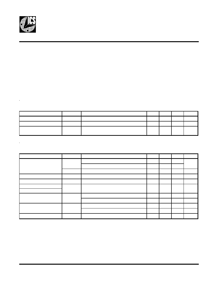
Absolute Maximum Ratings
Supply Voltage (VDD & AVDD) . . . . . . . . . . -0.5V to 3.6V
Logic Inputs . . . . . . . . . . . . . . . . . . . . . . . . . GND 0.5 V to V
DD
+0.5 V
Ambient Operating Temperature . . . . . . . . . 0°C to +85°C
Case Temperature . . . . . . . . . . . . . . . . . . . . 115°C
Storage Temperature . . . . . . . . . . . . . . . . . . 65°C to +150°C
Stresses above those listed under
Absolute Maximum Ratings may cause permanent damage to the device. These
ratings are stress specifications only and functional operation of the device at these or any other conditions above
those listed in the operational sections of the specifications is not implied. Exposure to absolute maximum rating
conditions for extended periods may affect product reliability.
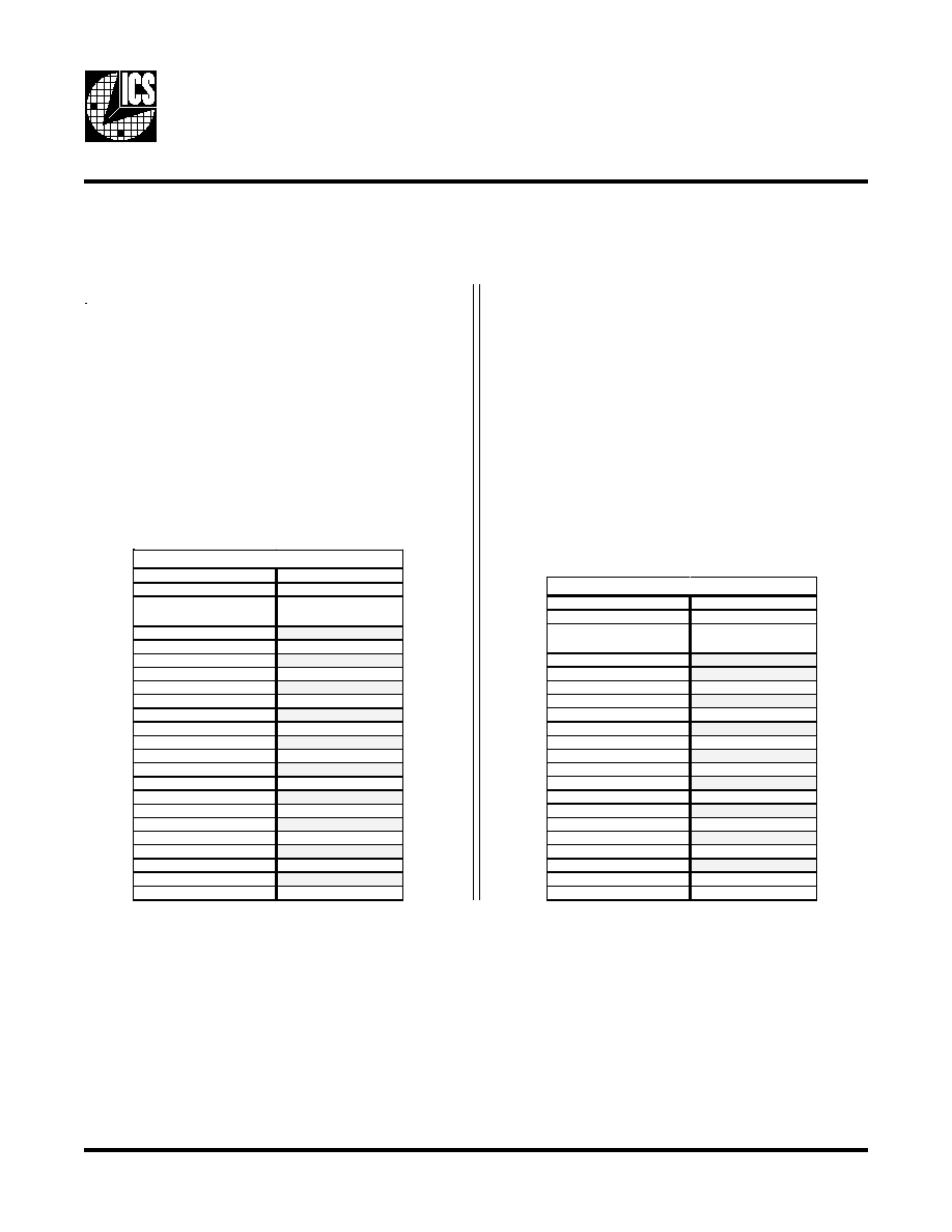
Electrical Characteristics - Input / Supply / Common Output parameters
T
A
= 0 - 70°C; Supply Voltage AV
DD
, V
DD
= 2.50V ± 0.20V (unless otherwise stated)
PARAMETER
SYMBOL
CONDITIONS
MIN
TYP
MAX
UNITS
R
T
= 120W, C
L
= 12 pF at 100MHz
236
300
R
T
= 120W, C
L
= 12 pF at 133MHz
263
300
I
DDPD
CL=0 pF
100
mA
Output High Current
I
OH
V
DD
= 2.5V, V
OUT
= 1V
-48
-33
-29
mA
Output Low Current
I
OL
V
DD
= 2.5V, V
OUT
= 1.2V
29
33
37
mA
High Impedance
Ouptut Current
V
DD
= min to max, I
OH
= -1mA
2
2.25
V
V
DD
= 2.3V, I
OH
= -12mA
1.95
V
DD
= min to max, I
OH
= 1mA
0.05
0.1
V
V
DD
= 2.3V, I
OH
= 12mA
0.3
0.4
Output Capacitance
1
C
OUT
V
I
= V
DD
or GND
3
pF
1. Guaranteed by design, not 100% tested in production.
Operating Supply Current
I
OZ
V
DD
= 2.7V, V
OUT
= V
DD
or GND
Low-level Output Voltage
V
OL
High-level Output Voltage
mA
10
V
OH
mA
I
DD2.5
Recommended Operation Conditions
T
A
= 0 - 70°C; Supply Voltage AV
DD
, V
DD
= 2.50V ± 0.20V (unless otherwise stated)
PARAMETER
SYMBOL
CONDITIONS
MIN
TYP
MAX
UNITS
Analog / Core Supply Volta
AV
DD
2.3
2.5
2.7
V
Input Voltage Level
V
IN
2
2.5
3
V
Output Differential Pair
Crossing Voltage
1.32
V
V
OC
66/100/133/166MHz, V
DD
=2.50V
1.23
1.25
4
ICS93732
0578H--02/19/04
Notes:
1.
Refers to transition on noninverting output.
2.
While the pulse skew is almost constant over frequency, the duty cycle error
increases at higher frequencies. This is due to the formula: duty cycle=t
wH
/t
c
, where
the cycle (t
c
) decreases as the frequency goes up.
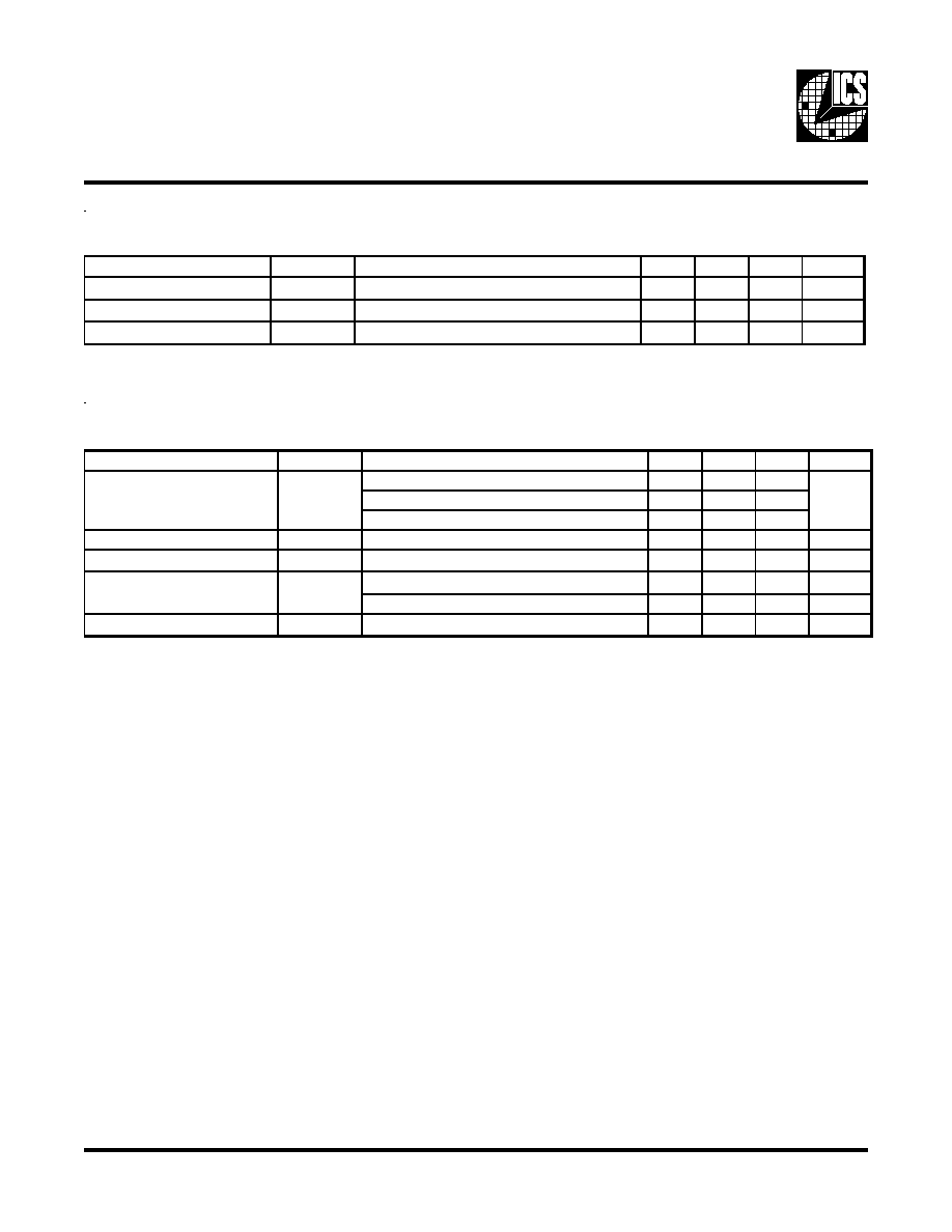
Timing Requirements
T
A
= 0 - 70°C; Supply Voltage AV
DD
, V
DD
= 2.50V (unless otherwise stated)
PARAMETER
SYMBOL
CONDITIONS
MIN
TYP
MAX
UNITS
Operating Clock Frequency
freq
op
Input Voltage level: 0-2.50V
22
340
MHz
Input Clock Duty Cycle
1
d
tin
40
50
60
%
Clock Stabilization
1
t
STAB
from VDD = 2.5V to 1% target frequency
100
µs
1. Guaranteed by design, not 100% tested in production.
Switching Characteristics
T
A
= 0 - 70°C; Supply Voltage AV
DD
, V
DD
= 2.50V ± 0.20V (unless otherwise stated)
PARAMETER
SYMBOL
CONDITIONS
MIN
TYP
MAX
UNITS
66 MHz
100
120
100 / 125/ 133/167MHz
48
65
200/267MHz
47
75
Phase Error
1
t
pe
-150
150
ps
Output to output Skew
1
T
skew
20
100
ps
66 MHz to 100MHz
49.5
50
50.5
%
101MHz to 267 MHz
49
49.4
51
%
Rise Time, Fall Time
4
t
R
, t
f
Load=120
/14pF 579
950
ps
ps
t
c-c
Duty Cycle (Sign Ended)
1,3
DC
Cycle to cycle Jitter
1,2
5
ICS93732
0578H--02/19/04
1.
The ICS clock generator is a slave/receiver, I
2
C component. It can read back the data stored in the latches
for verification. Read-Back will support Intel PIIX4 "Block-Read" protocol.
2.
The data transfer rate supported by this clock generator is 100K bits/sec or less (standard mode)
3.
The input is operating at 3.3V logic levels.
4.
The data byte format is 8 bit bytes.
5.
To simplify the clock generator I
2
C interface, the protocol is set to use only "Block-Writes" from the controller.
The bytes must be accessed in sequential order from lowest to highest byte with the ability to stop after any
complete byte has been transferred. The Command code and Byte count shown above must be sent, but the
data is ignored for those two bytes. The data is loaded until a Stop sequence is issued.
6.
At power-on, all registers are set to a default condition, as shown.
General I
2
C serial interface information
The information in this section assumes familiarity with I
2
C programming.
For more information, contact ICS for an I
2
C programming application note.
How to Write:
· Controller (host) sends a start bit.
· Controller (host) sends the write address D4
(H)
· ICS clock will acknowledge
· Controller (host) sends a dummy command code
· ICS clock will acknowledge
· Controller (host) sends a dummy byte count
· ICS clock will acknowledge
· Controller (host) starts sending first byte (Byte 0)
through byte 6
· ICS clock will acknowledge each byte one at a time.
· Controller (host) sends a Stop bit
How to Read:
· Controller (host) will send start bit.
· Controller (host) sends the read address D5
(H)
· ICS clock will acknowledge
· ICS clock will send the byte count
· Controller (host) acknowledges
· ICS clock sends first byte (Byte 0) through byte 6
· Controller (host) will need to acknowledge each byte
· Controller (host) will send a stop bit
Notes:
Controller (Host)
ICS (Slave/Receiver)
Start Bit
Address
D4
(H)
ACK
Dummy Command Code
ACK
Dummy Byte Count
ACK
Byte 0
ACK
Byte 1
ACK
Byte 2
ACK
Byte 3
ACK
Byte 4
ACK
Byte 5
ACK
Byte 6
ACK
Stop Bit
How to Write:
Controller (Host)
ICS (Slave/Receiver)
Start Bit
Address
D5
(H)
ACK
Byte Count
ACK
Byte 0
ACK
Byte 1
ACK
Byte 2
ACK
Byte 3
ACK
Byte 4
ACK
Byte 5
ACK
Byte 6
ACK
Stop Bit
How to Read: