 | –≠–ª–µ–∫—Ç—Ä–æ–Ω–Ω—ã–π –∫–æ–º–ø–æ–Ω–µ–Ω—Ç: ICS93776 | –°–∫–∞—á–∞—Ç—å:  PDF PDF  ZIP ZIP |
Integrated
Circuit
Systems, Inc.
ICS93776
0793A--03/08/05
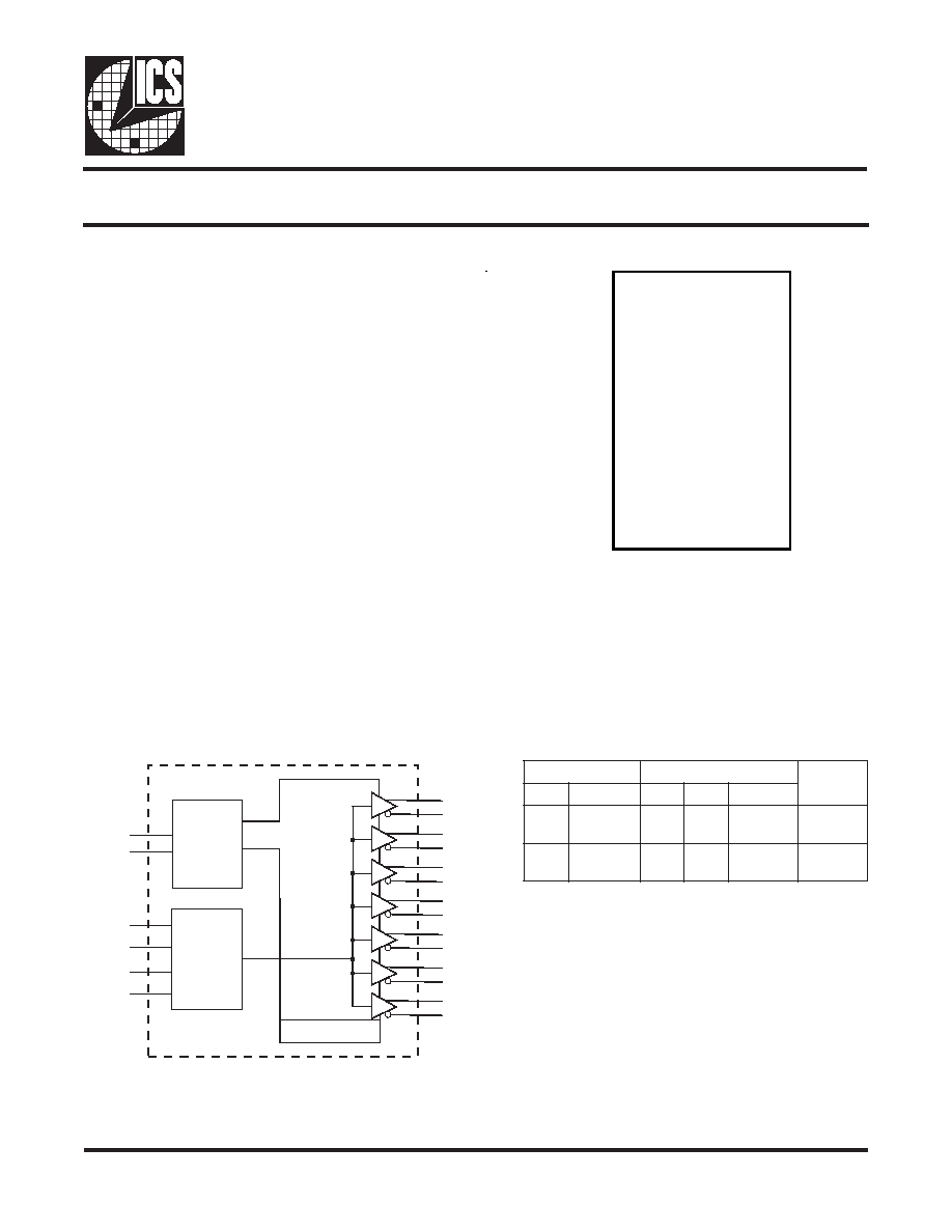
Block Diagram
Low Cost DDR Phase Lock Loop Zero Delay Buffer
Pin Configuration
Recommended Application:
DDR Zero Delay Clock Buffer
Product Description/Features:
∑
Low skew, low jitter PLL clock driver
∑
Max frequency supported = 266MHz (DDR 533)
∑
I
2
C for functional and output control
∑
Feedback pins for input to output synchronization
∑
Spread Spectrum tolerant inputs
∑
3.3V tolerant CLK_INT/C input
Switching Characteristics:
∑
CYCLE - CYCLE jitter: <100ps
∑
OUTPUT - OUTPUT skew: <100ps
∑
DUTY CYCLE: 48% - 52%
ADVANCE INFORMATION documents contain information on products in the formative or design phase development. Characteristic data and other specifications are design goals.
ICS reserves the right to change or discontinue these products without notice. Third party brands and names are the property of their respective owners.
DDRC0
1
28 GND
DDRT0
2
27 DDRC5
VDD
3
26 DDRT5
DDRT1
4
25 DDRC4
DDRC1
5
24 DDRT4
GND
6
23 VDD
SCLK
7
22 SDATA
CLK_INT
8
21 FB_INC
CLK_INC
9
20 FB_INT
VDDA 10
19 FB_OUTT
GND 11
18 FB_OUTC
VDD 12
17 DDRT3
DDRT2 13
16 DDRC3
DDRC2 14
15 GND
I
C
S
937
76
28-Pin 209mil SSOP
Functionality
S
T
U
P
N
I
S
T
U
P
T
U
O
e
t
a
t
S
L
L
P
D
D
V
A
T
N
I
_
K
L
C
T
K
L
C
C
K
L
C
T
T
U
O
_
B
F
V
5
.
2
)
m
o
n
(
L
L
H
L
n
o
V
5
.
2
)
m
o
n
(
H
H
L
H
n
o
FB_INT
FB_INC
CLK_INT
CLK_INC
SCLK
SCLK
SD
SDA
AT
TA
A
Control
Control
Logic
Logic
FB_OUTT
FB_OUTC
DDRC0
DDRC0
PLL
PLL
DDRT0
DDRT0
DDRC1
DDRC1
DDRT1
DDRT1
DDRC2
DDRC2
DDRT2
DDRT2
DDRC3
DDRC3
DDRT3
DDRT3
DDRC4
DDRC4
DDRT4
DDRT4
DDRC5
DDRC5
DDRT5
DDRT5

2
ICS93776
0793A--03/08/05
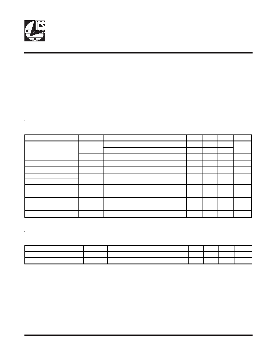
Pin Descriptions
PIN #
PIN NAME
PIN TYPE DESCRIPTION
1
DDRC0
OUT
"Complementary" Clock of differential pair output.
2
DDRT0
OUT
"True" Clock of differential pair output.
3
VDD
PWR
Power supply, nominal 2.5V
4
DDRT1
OUT
"True" Clock of differential pair output.
5
DDRC1
OUT
"Complementary" Clock of differential pair output.
6
GND
PWR
Ground pin.
7
SCLK
IN
Clock pin of SMBus circuitry, 5V tolerant.
8
CLK_INT
IN
"True" reference clock input.
9
CLK_INC
IN
"Complementary" reference clock input.
10
VDDA
PWR
2.5V power for the PLL core.
11
GND
PWR
Ground pin.
12
VDD
PWR
Power supply, nominal 2.5V
13
DDRT2
OUT
"True" Clock of differential pair output.
14
DDRC2
OUT
"Complementary" Clock of differential pair output.
15
GND
PWR
Ground pin.
16
DDRC3
OUT
"Complementary" Clock of differential pair output.
17
DDRT3
OUT
"True" Clock of differential pair output.
18
FB_OUTC
OUT
Complement single-ended feedback output, dedicated
external feedback. It switches at the same frequency
as other DDR outputs, This output must be connect to
FB_INC.
19
FB_OUTT
OUT
True single-ended feedback output, dedicated external
feedback. It switches at the same frequency as other
DDR outputs, This output must be connect to FB_INT.
20
FB_INT
IN
True single-ended feedback input, provides feedback
signal to internal PLL for synchronization with
CLK_INT to eliminate phase error.
21
FB_INC
IN
Complement single-ended feedback input, provides
feedback signal to internal PLL for synchronization
with CLK_INT to eliminate phase error.
22
SDATA
I/O
Data pin for SMBus circuitry, 5V tolerant.
23
VDD
PWR
Power supply, nominal 2.5V
24
DDRT4
OUT
"True" Clock of differential pair output.
25
DDRC4
OUT
"Complementary" Clock of differential pair output.
26
DDRT5
OUT
"True" Clock of differential pair output.
27
DDRC5
OUT
"Complementary" Clock of differential pair output.
28
GND
PWR
Ground pin.
3
ICS93776
0793A--03/08/05
Absolute Maximum Ratings
Supply Voltage (VDD & AVDD) . . . . . . . . . . -0.5V to 3.6V
Logic Inputs . . . . . . . . . . . . . . . . . . . . . . . . . GND ≠0.5 V to V
DD
+0.5 V
Ambient Operating Temperature . . . . . . . . . 0∞C to +85∞C
Storage Temperature . . . . . . . . . . . . . . . . . . ≠65∞C to +150∞C
Stresses above those listed under
Absolute Maximum Ratings may cause permanent damage to the device. These
ratings are stress specifications only and functional operation of the device at these or any other conditions above
those listed in the operational sections of the specifications is not implied. Exposure to absolute maximum rating
conditions for extended periods may affect product reliability.
Electrical Characteristics - Input / Supply / Common Output parameters
T
A
= 0 - 70∞C; Supply Voltage AV
DD
, V
DD
= 2.50V ± 0.20V (unless otherwise stated)
PARAMETER
SYMBOL
CONDITIONS
MIN
TYP
MAX
UNITS
R
T
= 120W, C
L
= 12 pF at 100MHz
300
R
T
= 120W, C
L
= 12 pF at 133MHz
300
I
DDPD
CL=0 pF
100
mA
Output High Current
I
OH
V
DD
= 2.5V, V
OUT
= 1V
-48
-29
mA
Output Low Current
I
OL
V
DD
= 2.5V, V
OUT
= 1.2V
29
37
mA
High Impedance
Ouptut Current
V
DD
= min to max, I
OH
= -1mA
2
V
V
DD
= 2.3V, I
OH
= -12mA
V
DD
= min to max, I
OH
= 1mA
0.1
V
V
DD
= 2.3V, I
OH
= 12mA
0.4
Output Capacitance
1
C
OUT
V
I
= V
DD
or GND
pF
1. Guaranteed by design, not 100% tested in production.
mA
10
V
OH
mA
I
DD2.5
Operating Supply Current
I
OZ
V
DD
= 2.7V, V
OUT
= V
DD
or GND
Low-level Output Voltage
V
OL
High-level Output Voltage
Recommended Operation Conditions
T
A
= 0 - 70∞C; Supply Voltage AV
DD
, V
DD
= 2.50V ± 0.20V (unless otherwise stated)
PARAMETER
SYMBOL
CONDITIONS
MIN
TYP
MAX
UNITS
Analog / Core Supply Voltage
AV
DD
2.3
2.7
V
Input Voltage Level
V
IN
2
3
V
4
ICS93776
0793A--03/08/05
Timing Requirements
T
A
= 0 - 70∞C; Supply Voltage AV
DD
, V
DD
= 2.50V (unless otherwise stated)
PARAMETER
SYMBOL
CONDITIONS
MIN
TYP
MAX
UNITS
Operating Clock Frequency
1
freq
op
Input Voltage level: 0-2.50V
22
340
MHz
Input Clock Duty Cycle
1
d
tin
40
50
60
%
Clock Stabilization
1
t
STAB
from VDD = 2.5V to 1% target frequency
100
µs
1. Guaranteed by design, not 100% tested in production.
Switching Characteristics
T
A
= 0 - 70∞C; Supply Voltage AV
DD
, V
DD
= 2.50V ± 0.20V (unless otherwise stated)
PARAMETER
SYMBOL
CONDITIONS
MIN
TYP
MAX
UNITS
66 MHz to 266 MHz
100
Phase Error
1
t
pe
-150
150
ps
Output to output Skew
1
T
skew
100
ps
Duty Cycle (Sign Ended)
1,3
DC
66 MHz to 267 MHz
48
52
%
Rise Time, Fall Time
4
t
R
, t
f
Load=120
/14pF
950
ps
Output Differential Pair
Crossing Voltage
1. Guaranteed by design, not 100% tested in production.
2. Refers to transistion on non-inverting period.
3. While the pulse skew is almost constant over frequency, the duty cycle error increases at higher frequencies.
This is due to the formular: duty_cycle=t
wH
/t
C
, where the cycle time (t
C
)decreases as the frequency increases.
ps
t
c-c
Cycle to cycle Jitter
1,2
1.32
V
V
OC
V
DD
=2.50V
1.23
5
ICS93776
0793A--03/08/05
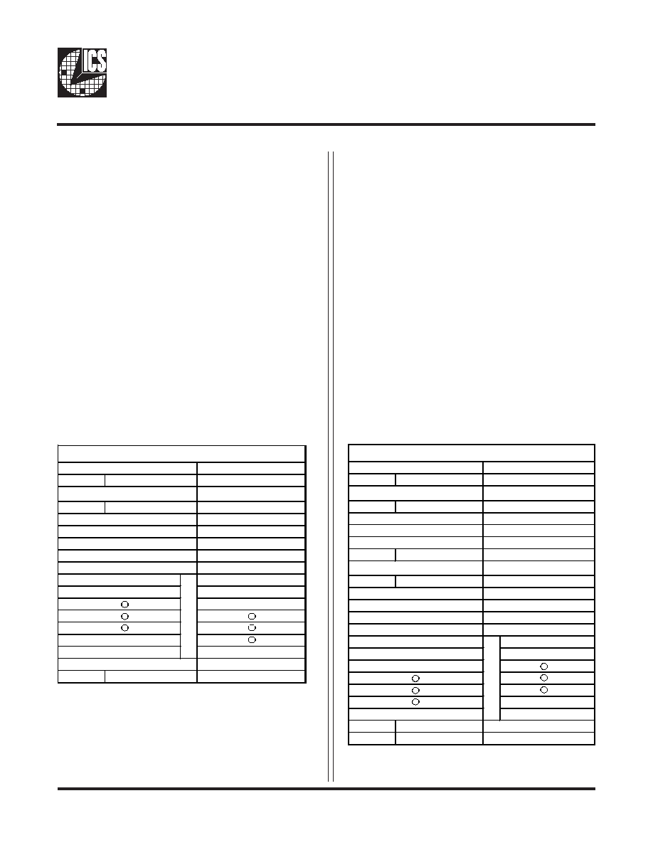
General SMBus serial interface information
How to Write:
∑ Controller (host) sends a start bit.
∑ Controller (host) sends the write address D4
(H)
∑ ICS clock will
acknowledge
∑ Controller (host) sends the begining byte location = N
∑ ICS clock will
acknowledge
∑ Controller (host) sends the data byte count = X
∑ ICS clock will
acknowledge
∑ Controller (host) starts sending
Byte N through
Byte N + X -1
(see Note 2)
∑ ICS clock will
acknowledge each byte one at a time
∑ Controller (host) sends a Stop bit
How to Read:
∑ Controller (host) will send start bit.
∑ Controller (host) sends the write address D4
(H)
∑ ICS clock will
acknowledge
∑ Controller (host) sends the begining byte
location = N
∑ ICS clock will
acknowledge
∑ Controller (host) will send a separate start bit.
∑ Controller (host) sends the read address D5
(H)
∑ ICS clock will
acknowledge
∑ ICS clock will send the data byte count = X
∑ ICS clock sends
Byte N + X -1
∑ ICS clock sends
Byte 0 through byte X (if X
(H)
was written to byte 8)
.
∑ Controller (host) will need to acknowledge each byte
∑ Controllor (host) will send a not acknowledge bit
∑ Controller (host) will send a stop bit
ICS (Slave/Receiver)
T
W R
ACK
ACK
ACK
ACK
ACK
P
Byte N + X - 1
Data Byte Count = X
Beginning Byte N
stoP bit
X Byte
Index Block Write Operation
Slave Address D4
(H )
Beginning Byte = N
W Rite
starT bit
Controller (Host)
T
starT bit
W R
W Rite
RT
Repeat starT
RD
ReaD
Beginning Byte N
Byte N + X - 1
N
Not acknowledge
P
stoP bit
ICS (Slave/Rece iver)
Controller (Host)
X Byte
ACK
ACK
Data Byte Count = X
ACK
Slave Address D5
(H )
Index Block Read Operation
Slave Address D4
(H )
Beginning Byte = N
ACK
ACK