 | ÐлекÑÑоннÑй компоненÑ: ICS93857 | СкаÑаÑÑ:  PDF PDF  ZIP ZIP |
/home/web/doc/html/icst/173761
Integrated
Circuit
Systems, Inc.
ICS93857
Preliminary Product Preview
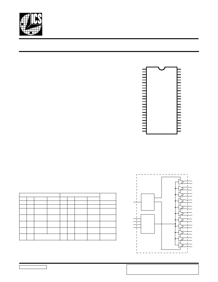
Block Diagram
DDR Phase Lock Loop Clock Driver
93857 Rev C 11/03/00
Pin Configuration
48-Pin TSSOP
Recommended Application:
DDR Memory Modules
Product Description/Features:
Low skew, low jitter PLL clock driver
1 to 10 differential clock distribution
Feedback pins for input to output synchronization
Active high OE to enable outputs
Spread Spectrum tolerant inputs
Specifications:
Input/Output Level
Inputs and outputs are compatible to JEDEC SSTL-2
standard.
Switching Characteristics:
PEAK - PEAK jitter (66MHz): <120ps
PEAK - PEAK jitter (>100MHz): <75ps
CYCLE - CYCLE jitter (66MHz):<120ps
CYCLE - CYCLE jitter (>100MHz):<65ps
OUTPUT - OUTPUT skew: <100ps
Output Rise and Fall Time: 650ps - 950ps
DUTY CYCLE: 49.5% - 50.5%
GND
CLKC0
CLKT0
VDD
CLKT1
CLKC1
GND
GND
CLKC2
CLKT2
VDD
VDD
CLK_INT
CLK_INC
VDD
AVDD
AGND
GND
CLKC3
CLKT3
VDD
CLKT4
CLKC4
GND
GND
CLKC5
CLKT5
VDD
CLKT6
CLKC6
GND
GND
CLKC7
CLKT7
VDD
OE
FB_INT
FB_INC
VDD
FB_OUTC
FB_OUTT
GND
CLKC8
CLKT8
VDD
CLKT9
CLKC9
GND
ICS93857
1
2
3
4
5
6
7
8
9
10
11
12
13
14
15
16
17
18
19
20
21
22
23
24
48
47
46
45
44
43
42
41
40
39
38
37
36
35
34
33
32
31
30
29
28
27
26
25
S
T
U
P
N
I
S
T
U
P
T
U
O
e
t
a
t
S
L
L
P
D
D
V
A
E
O
T
N
I
_
K
L
C
C
N
I
_
K
L
C
T
K
L
C
C
K
L
C
T
T
U
O
_
B
F
C
T
U
O
_
B
F
D
N
G
H
L
H
L
H
L
H
f
f
o
/
d
e
s
s
a
p
y
B
D
N
G
H
H
L
H
L
H
L
f
f
o
/
d
e
s
s
a
p
y
B
V
5
.
2
)
m
o
n
(
L
L
H
Z
Z
Z
Z
f
f
o
V
5
.
2
)
m
o
n
(
L
H
L
Z
Z
Z
Z
f
f
o
V
5
.
2
)
m
o
n
(
H
L
H
L
H
L
H
n
o
V
5
.
2
)
m
o
n
(
H
H
L
H
L
H
L
n
o
V
5
.
2
)
m
o
n
(
X
)
z
H
M
0
2
<
)
1
(
Z
Z
Z
Z
f
f
o
Functionality
PLL
FB_INT
FB_INC
CLK_INC
CLK_INT
OE
Control
Logic
FB_OUTT
FB_OUTC
CLKT0
CLKT1
CLKT2
CLKT3
CLKT4
CLKT5
CLKT6
CLKT7
CLKT8
CLKT9
CLKC0
CLKC1
CLKC2
CLKC3
CLKC4
CLKC5
CLKC6
CLKC7
CLKC8
CLKC9
PRODUCT PREVIEW documents contain information on new
products in the sampling or preproduction phase of development.
Characteristic data and other specifications are subject to change
without notice.
2
ICS93857
Preliminary Product Preview
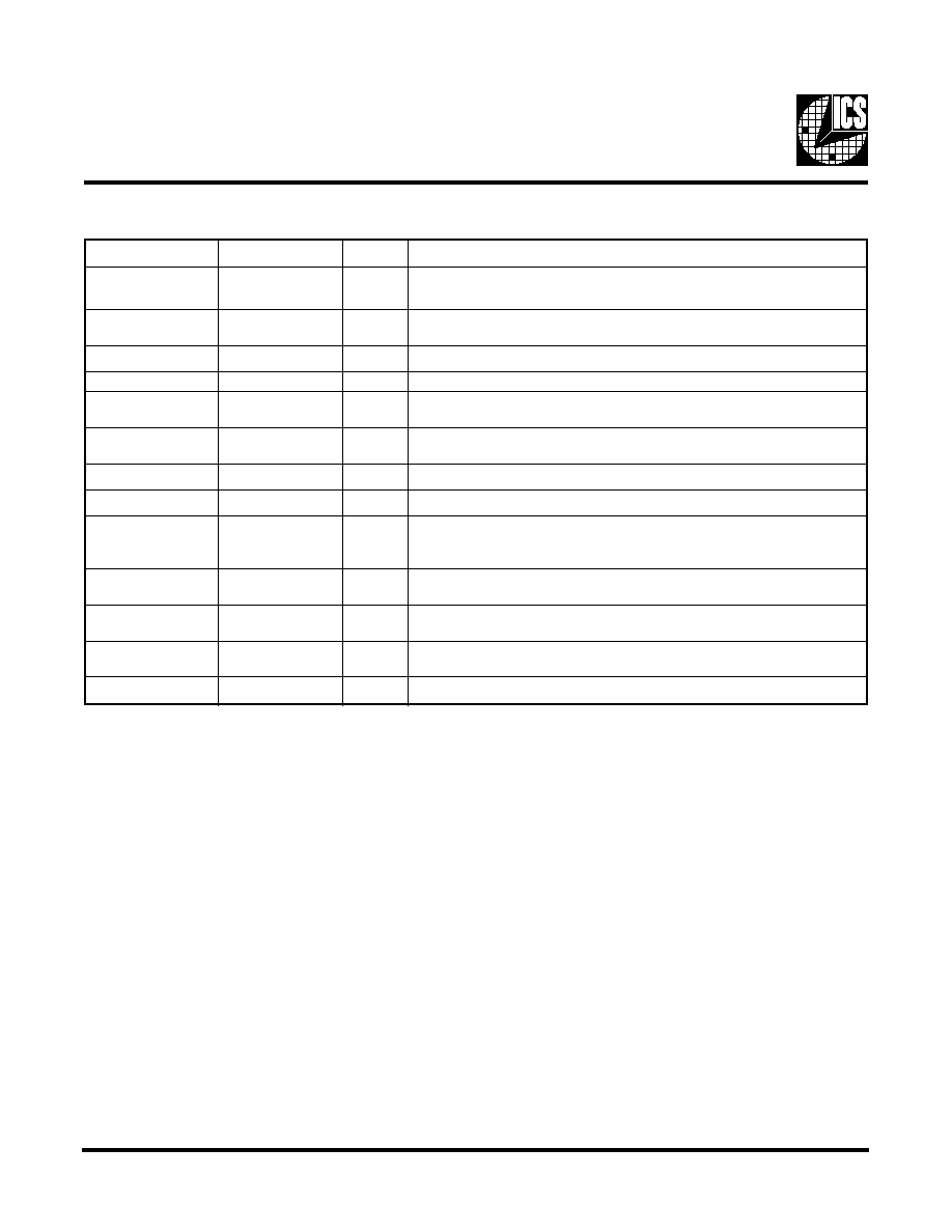
Pin Descriptions
R
E
B
M
U
N
N
I
P
E
M
A
N
N
I
P
E
P
Y
T
N
O
I
T
P
I
R
C
S
E
D
,
8
2
,
1
2
,
5
1
,
2
1
,
1
1
,
4
,
5
4
,
8
3
,
4
3
D
D
V
R
W
P
V
5
.
2
y
l
p
p
u
s
r
e
w
o
P
,
5
2
,
4
2
,
8
1
,
8
,
7
,
1
8
4
,
2
4
,
1
4
,
1
3
D
N
G
R
W
P
d
n
u
o
r
G
6
1
D
D
V
A
R
W
P
V
5
.
2
,
y
l
p
p
u
s
r
e
w
o
p
g
o
l
a
n
A
7
1
D
N
G
A
R
W
P
.
d
n
u
o
r
g
g
o
l
a
n
A
,
6
4
,
4
4
,
9
3
,
9
2
,
7
2
3
,
5
,
0
1
,
0
2
,
2
2
)
0
:
9
(
T
K
L
C
T
U
O
.
s
t
u
p
t
u
o
r
i
a
p
l
a
i
t
n
e
r
e
f
f
i
d
f
o
k
c
o
l
C
"
e
u
r
T
"
,
7
4
,
3
4
,
0
4
,
0
3
,
6
2
2
,
6
,
9
,
9
1
,
3
2
)
0
:
9
(
C
K
L
C
T
U
O
.
s
t
u
p
t
u
o
r
i
a
p
l
a
i
t
n
e
r
e
f
f
i
d
f
o
s
k
c
o
l
c
"
y
r
o
t
n
e
m
e
l
p
m
o
C
"
4
1
C
N
I
_
K
L
C
N
I
t
u
p
n
i
k
c
o
l
c
e
c
n
e
r
e
f
e
r
"
y
r
o
t
n
e
m
e
l
p
m
o
C
"
3
1
T
N
I
_
K
L
C
N
I
t
u
p
n
i
k
c
o
l
c
e
c
n
e
r
e
f
e
r
"
e
u
r
T
"
3
3
C
T
U
O
_
B
F
T
U
O
t
I
.
k
c
a
b
d
e
e
f
l
a
n
r
e
t
x
e
r
o
f
d
e
t
a
c
i
d
e
d
,
t
u
p
t
u
o
k
c
a
b
d
e
e
F
"
y
r
o
t
n
e
m
e
l
p
m
o
C
"
o
t
d
e
r
i
w
e
b
t
s
u
m
t
u
p
t
u
o
s
i
h
T
.
K
L
C
e
h
t
s
a
y
c
n
e
u
q
e
r
f
e
m
a
s
e
h
t
t
a
s
e
h
c
t
i
w
s
.
C
N
I
_
B
F
2
3
T
T
U
O
_
B
F
T
U
O
e
h
t
t
a
s
e
h
c
t
i
w
s
t
I
.
k
c
a
b
d
e
e
f
l
a
n
r
e
t
x
e
r
o
f
d
e
t
a
c
i
d
e
d
,
t
u
p
t
u
o
k
c
a
b
d
e
e
F
"
"
e
u
r
T
"
.
T
N
I
_
B
F
o
t
d
e
r
i
w
e
b
t
s
u
m
t
u
p
t
u
o
s
i
h
T
.
K
L
C
e
h
t
s
a
y
c
n
e
u
q
e
r
f
e
m
a
s
6
3
T
N
I
_
B
F
N
I
r
o
f
L
L
P
l
a
n
r
e
t
n
i
e
h
t
o
t
l
a
n
g
i
s
k
c
a
b
d
e
e
f
s
e
d
i
v
o
r
p
,
t
u
p
n
i
k
c
a
b
d
e
e
F
"
e
u
r
T
"
.
r
o
r
r
e
e
s
a
h
p
e
t
a
n
i
m
i
l
e
o
t
T
N
I
_
K
L
C
h
t
i
w
n
o
i
t
a
z
i
n
o
r
h
c
n
y
s
5
3
C
N
I
_
B
F
N
I
r
o
f
L
L
P
l
a
n
r
e
t
n
i
e
h
t
o
t
l
a
n
g
i
s
s
e
d
i
v
o
r
p
,
t
u
p
n
i
k
c
a
b
d
e
e
F
"
y
r
o
t
n
e
m
e
l
p
m
o
C
"
.
r
o
r
r
e
e
s
a
h
p
e
t
a
n
i
m
i
l
e
o
t
C
N
I
_
K
L
C
h
t
i
w
n
o
i
t
a
z
i
n
o
r
h
c
n
y
s
7
3
E
O
N
I
n
i
p
e
l
b
a
n
e
t
u
p
t
u
o
h
g
i
H
e
v
i
t
c
A
3
ICS93857
Preliminary Product Preview
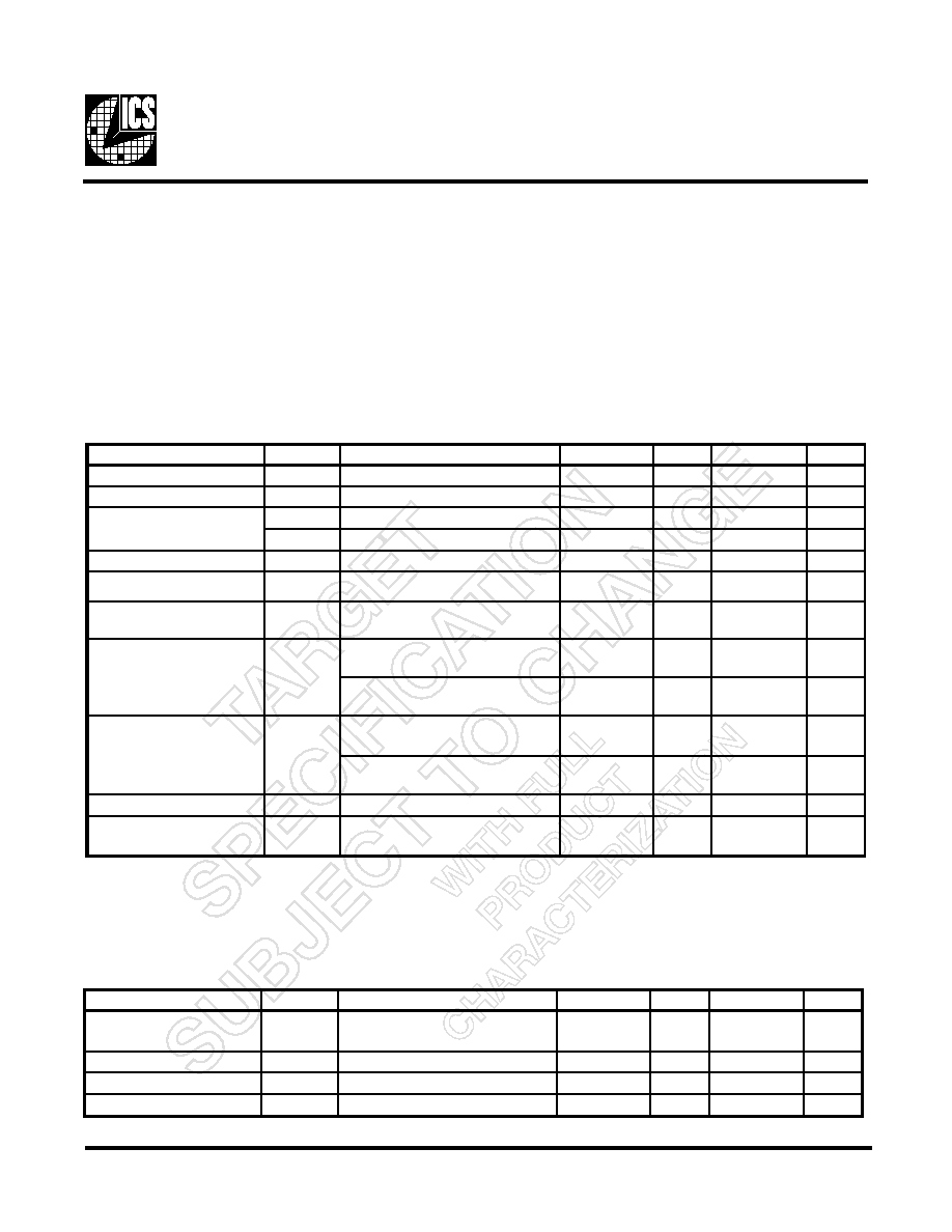
Absolute Maximum Ratings
Supply Voltage (VDD & AVDD) . . . . . . . . . . . . . -0.5V to 4.6V
Logic Inputs . . . . . . . . . . . . . . . . . . . . . . . . . . . . GND 0.5 V to V
DD
+0.5 V
Ambient Operating Temperature . . . . . . . . . . . . 0°C to +85°C
Storage Temperature . . . . . . . . . . . . . . . . . . . . . . 65°C to +150°C
Stresses above those listed under Absolute Maximum Ratings may cause permanent damage to the device. These ratings are
stress specifications only and functional operation of the device at these or any other conditions above those listed in the
operational sections of the specifications is not implied. Exposure to absolute maximum rating conditions for extended periods
may affect product reliability.
Recommended Operating Condition
T
A
= 0 - 85C; Supply Voltage AVDD, VDD = 2.5 V +/- 0.2V (unless otherwise stated)
PARAMETER
SYMBOL
CONDITIONS
MIN
TYP
MAX
UNITS
Analog/core supply voltage
A
VDD
2.3
2.5
2.7
V
Input High Voltage
V
IH
OE input
0.7 x V
DD
V
Input Low Voltage
V
IL
OE input
0.3 x V
DD
V
Input voltage level
V
IN
-0.3
V
DD
+0.3
V
1
Guaranteed by design, not 100% tested in production.
Electrical Characteristics - Input/Supply/Common Output Parameters
T
A
= 0 - 85C; Supply Voltage AVDD, VDD = 2.5 V +/- 0.2V (unless otherwise stated)
PARAMETER
SYMBOL
CONDITIONS
MIN
TYP
MAX
UNITS
Input Current
I
IH
VI = VDD or GND
±10
µA
Input Low Current
I
IL
VI = VDD or GND
±10
µA
I
DD2.5
CL = 0pf
250
mA
I
DDPD
CL = 0pf
50
100
µ
A
Output High Current
I
OH
VDD = 2.3V, V
OUT
= 1V
-18
-32
mA
Output Low Current
I
OL
VDD = 2.3V, V
OUT
= 1.2V
26
30
mA
High Impedance
Output Current
I
OZ
VDD=2.7V, Vout=VDD or GND
±10
µ
A
VDD = min to max,
IOH = -1 mA
VDD -0.1
V
VDD = 2.3V,
IOH = -12 mA
1.7
V
VDD = min to max
I
OL
=1 mA
0.1
VDD = 2.3V
IOH=12 mA
0.6
V
Input Capacitance
1
C
IN
VI = GND or VDD
9
pF
Output differential-pair
crossing voltage
V
OC
(V
DD
/2) -0.2
V
DD
/2
(V
DD
/2) +0.2
V
1
Guaranteed by design, not 100% tested in production.
Operating Supply Current
High-level output voltage
V
OH
Low-level output voltage
V
OL
4
ICS93857
Preliminary Product Preview
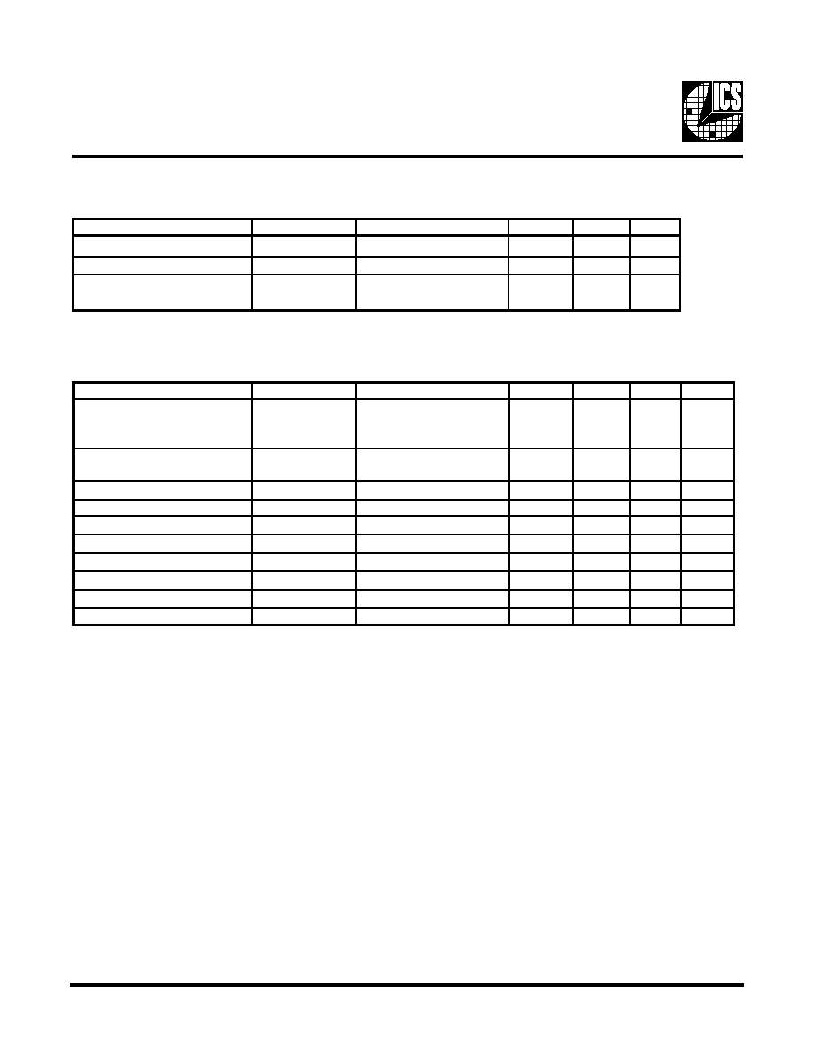
Notes:
1. Refers to transition on noninverting output in PLL bypass mode.
Tim ing Re quire m e nts
T
A
= 0 - 8 5 C ; Su p p ly Vo ltag e AVDD, VDD = 2 .5 V +/- 0 .2 V (u n less o th erwise stated )
PAR AM ETER
SYM B OL
C ONDITIONS
M IN
M AX
UNITS
Op eratin g clo ck freq u en cy
freq
o p
6 6
1 7 0
M Hz
In p u t clo ck d u ty cy cle
d
t in
4 0
6 0
%
C LK stab ilizatio n
T
STAB
fro m VDD = 3 .3 V to 1 %
targ et freq .
1 0 0
µ s
Switching Characteristics
PARAMETER
SYMBOL
CONDITION
MIN
TYP
MAX
UNITS
Low-to high level propagation
delay time, bypass mode
t
PLH
1
CLK_IN to any output
1.5
3.5
6
ns
High-to low level propagation
delay time
t
PLL
1
CLK_IN to any output
1.5
3.5
6
ns
Output enable time
t
EN
OE to any output
3
ns
Output disable time
tdis
OE to any output
3
ns
Jitter; peak to peak jitter
T
jitter
100/125/133/167MHz
75
ps
Cycle to Cycle Jitter1
T
cyc
-T
cyc
100/125/133/167MHz
75
ps
Phase error, static
t
(phase error)
-150
150
ps
Output to Output Skew
T
skew
100
ps
Duty cycle
D
C
2
100MHz to 167MHz
49
51
%
Rise Time, Fall Time
tr, tf
Load = 120
/16pF
800
950
ps
5
ICS93857
Preliminary Product Preview
Ordering Information
ICS93857yGT
Designation for tape and reel packaging
Pattern Number (2 or 3 digit number for parts with ROM code patterns)
Package Type
G=TSSOP
Revision Designator (will not correlate with datasheet revision)
Device Type (consists of 3 or 4 digit numbers)
Prefix
ICS, AV = Standard Device
Example:
ICS XXXX y G - PPP - T
PRODUCT PREVIEW documents contain information on new
products in the sampling or preproduction phase of development.
Characteristic data and other specifications are subject to change
without notice.
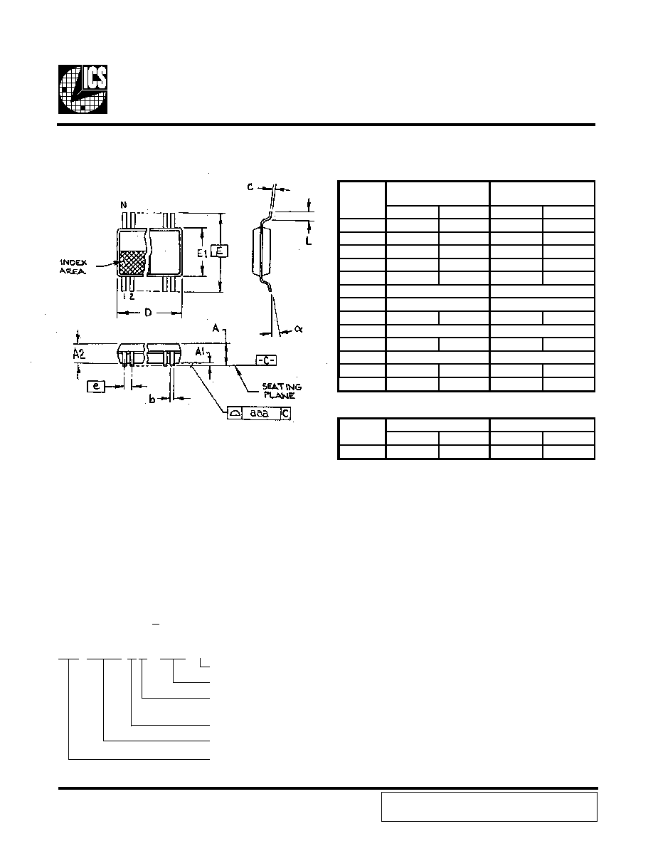
6.10 mm. Body, 0.50 mm. pitch TSSOP
(240 mil)
(0.020 mil)
MIN
MAX
MIN
MAX
A
-
1.20
-
.047
A1
0.05
0.15
.002
.006
A2
0.80
1.05
.032
.041
b
0.17
0.27
.007
.011
c
0.09
0.20
.0035
.008
D
E
E1
6.00
6.20
.236
.244
e
0.50 BASIC
0.020 BASIC
L
0.45
0.75
.018
.30
N
0°
8°
0°
8°
aaa
-
0.10
-
.004
VARIATIONS
MIN
MAX
MIN
MAX
48
12.40
12.60
.488
.496
MO-153 JEDEC
Doc.# 10-0039
7/6/00 Rev B
SYMBOL
SEE VARIATIONS
SEE VARIATIONS
In Millimeters
COMMON DIMENSIONS
In Inches
COMMON DIMENSIONS
SEE VARIATIONS
8.10 BASIC
0.319
N
D mm.
D (inch)
SEE VARIATIONS