Integrated
Circuit
Systems, Inc.
ICS94201
94201 Rev A - 05/24/01
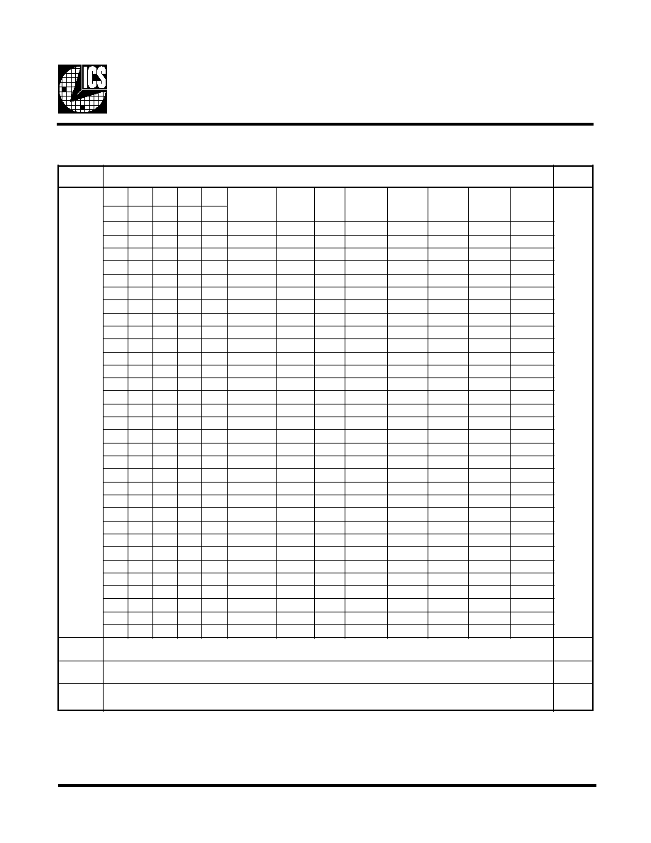
Pin Configuration
Recommended Application:
810/810E and Solano (815) type chipset
Output Features:
∑
2 - CPUs @ 2.5V
∑
13 - SDRAM @ 3.3V
∑
3 - 3V66 @ 3.3V
∑
8 - PCI @3.3V
∑
1 - 24/48MHz@ 3.3V
∑
1 - 48MHz @ 3.3V fixed
∑
1 - REF @3.3V, 14.318MHz
Features:
∑
Programmable ouput frequency.
∑
Programmable ouput rise/fall time for PCI
and SDRAM clocks.
∑
Programmable 3V66 to PCI skew.
∑
Spread spectrum for EMI control
with programmable spread percentage.
∑
Watchdog timer technology to reset system
if over-clocking causes malfunction.
∑
Support power management through PD#.
∑
Uses external 14.318MHz crystal.
∑
FS pins for frequency select
Key Specifications:
∑
CPU Output Jitter: <250ps
∑
IOAPIC Output Jitter: <500ps
∑
48MHz, 3V66, PCI Output Jitter: <500ps
∑
CPU Output Skew: <175ps
∑
PCI Output Skew: <500ps
∑
3V66 Output Skew <175ps
∑
For group skew timing, please refer to the
Group Timing Relationship Table.
Programmable System Frequency Generator for P
II
/
III
TM
56-Pin 300 mil SSOP
1. These pins will have 1.5 to 2X drive strength.
* 120K ohm pull-up to VDD on indicated inputs.
PLL2
PLL1
Spread
Spectrum
48MHz
24_48MHz
CPUCLK [1:0]
2
12
8
3
SDRAM [11:0]
IOAPIC
PCICLK [7:0]
SDRAM_F
3V66 [2:0]
X1
X2
XTAL
OSC
CPU
DIVDER
SDRAM
DIVDER
IOAPIC
DIVDER
PCI
DIVDER
3V66
DIVDER
FS[4:0]
PD#
SEL24_48#
SDATA
SCLK
Control
Logic
Config.
Reg.
/ 2
REF0
Block Diagram
VDDREF
X1
X2
GNDREF
GND3V66
3V66-1
3V66-2
VDD3V66
VDDPCI
*(FS0)PCICLK0
*(FS1)PCICLK1
*(SEL24_48#)PCICLK2
GNDPCI
PCICLK3
PCICLK4
PCICLK5
VDDPCI
PCICLK6
PCICLK7
GNDPCI
PD#
SCLK
SDATA
VDDSDR
SDRAM11
SDRAM10
GNDSDR
3V66-0
1
1
1
REF0(FS4)*
VDDLAPIC
IOAPIC
VDDLCPU
CPUCLK0
CPUCLK1
GNDLCPU
GNDSDR
SDRAM0
SDRAM1
SDRAM2
VDDSDR
SDRAM3
SDRAM4
SDRAM5
GNDSDR
SDRAM6
SDRAM7
SDRAM_F
VDDSDR
GND48
24_48MHz(FS2)*
48MHz(FS3)*
VDD48
VDDSDR
SDRAM8
SDRAM9
GNDSDR
1
1
ICS94201
1
2
3
4
5
6
7
8
9
10
11
12
13
14
15
16
17
18
19
20
21
22
23
24
25
26
27
28
56
55
54
53
52
51
50
49
48
47
46
45
44
43
42
41
40
39
38
37
36
35
34
33
32
31
30
29
ICS reserves the right to make changes in the device data identified in
this publication without further notice. ICS advises its customers to
obtain the latest version of all device data to verify that any
information being relied upon by the customer is current and accurate.
2
ICS94201
General Description
Pin Configuration
The ICS94201 is a single chip clock solution for desktop designs using the 810/810E and Solano style chipset. It provides all necessary
clock signals for such a system.
The ICS94201 belongs to ICS new generation of programmable system clock generators. It employs serial programming I
2
C interface
as a vehicle for changing output functions, changing output frequency, configuring output strength, configuring output to output skew,
changing spread spectrum amount, changing group divider ratio and dis/enabling individual clocks. This device also has ICS
propriety 'Watchdog Timer' technology which will reset the frequency to a safe setting if the system become unstable from over
clocking.
Spread spectrum typically reduces system EMI by 7dB to 8dB. This simplifies EMI qualification without resorting to board design
iterations or costly shielding.
N
I
P
R
E
B
M
U
N
E
M
A
N
N
I
P
E
P
Y
T
N
O
I
T
P
I
R
C
S
E
D
,
5
2
,
8
1
,
0
1
,
9
,
1
5
4
,
7
3
,
3
3
,
2
3
D
D
V
R
W
P
y
l
p
p
u
s
r
e
w
o
p
V
3
.
3
2
1
X
N
I
k
c
a
b
d
e
e
f
d
n
a
)
F
p
3
3
(
p
a
c
d
a
o
l
l
a
n
r
e
t
n
i
s
a
h
,t
u
p
n
i
l
a
t
s
y
r
C
2
X
m
o
r
f
r
o
t
s
i
s
e
r
3
2
X
T
U
O
d
a
o
l
l
a
n
r
e
t
n
i
s
a
H
.
z
H
M
8
1
3
.
4
1
y
ll
a
n
i
m
o
n
,t
u
p
t
u
o
l
a
t
s
y
r
C
)
F
p
3
3
(
p
a
c
,
1
2
,
4
1
,
5
,
4
,
6
3
,
9
2
,
8
2
9
4
,
1
4
D
N
G
R
W
P
y
l
p
p
u
s
V
3
.
3
r
o
f
s
n
i
p
d
n
u
o
r
G
6
,
7
,
8
]
0
:
2
[
6
6
V
3
T
U
O
B
U
H
r
o
f
s
t
u
p
t
u
o
k
c
o
l
c
z
H
M
6
6
d
e
x
i
F
V
3
.
3
1
1
0
K
L
C
I
C
P
1
T
U
O
s
K
L
C
U
P
C
s
u
o
n
o
r
h
c
n
y
S
h
ti
w
,t
u
p
t
u
o
k
c
o
l
c
I
C
P
V
3
.
3
0
S
F
N
I
.
n
o
r
e
w
o
p
t
a
d
e
h
c
t
a
l
t
u
p
n
I
.t
i
b
t
c
e
l
e
s
y
c
n
e
u
q
e
r
f
t
u
p
n
i
c
i
g
o
L
2
1
1
K
L
C
I
C
P
1
T
U
O
s
K
L
C
U
P
C
s
u
o
n
o
r
h
c
n
y
S
h
ti
w
,t
u
p
t
u
o
k
c
o
l
c
I
C
P
V
3
.
3
1
S
F
N
I
.
n
o
r
e
w
o
p
t
a
d
e
h
c
t
a
l
t
u
p
n
I
.t
i
b
t
c
e
l
e
s
y
c
n
e
u
q
e
r
f
t
u
p
n
i
c
i
g
o
L
3
1
#
8
4
_
4
2
_
L
E
S
N
I
.
t
u
p
t
u
o
t
c
e
l
e
s
o
t
t
u
p
n
i
c
i
g
o
L
2
K
L
C
I
C
P
1
T
U
O
s
K
L
C
U
P
C
s
u
o
n
o
r
h
c
n
y
S
h
ti
w
,t
u
p
t
u
o
k
c
o
l
c
I
C
P
V
3
.
3
,
7
1
,
9
1
,
0
2
5
1
,
6
1
]
3
:
7
[
K
L
C
I
C
P
T
U
O
s
K
L
C
U
P
C
s
u
o
n
o
r
h
c
n
y
S
h
ti
w
,
s
t
u
p
t
u
o
k
c
o
l
c
I
C
P
V
3
.
3
2
2
#
D
P
N
I
a
o
t
n
i
e
c
i
v
e
d
e
h
t
n
w
o
d
r
e
w
o
p
o
t
d
e
s
u
n
i
p
t
u
p
n
i
w
o
l
e
v
it
c
a
s
u
o
n
o
r
h
c
n
y
s
A
e
h
t
d
n
a
O
C
V
e
h
t
d
n
a
d
e
l
b
a
s
i
d
e
r
a
s
k
c
o
l
c
l
a
n
r
e
t
n
i
e
h
T
.
e
t
a
t
s
r
e
w
o
p
w
o
l
r
e
t
a
e
r
g
e
b
t
o
n
ll
i
w
n
w
o
d
r
e
w
o
p
e
h
t
f
o
y
c
n
e
t
a
l
e
h
T
.
d
e
p
p
o
t
s
e
r
a
l
a
t
s
y
r
c
.
s
m
3
n
a
h
t
3
2
K
L
C
S
N
I
I
f
o
t
u
p
n
i
k
c
o
l
C
2
t
u
p
n
i
C
4
2
A
T
A
D
S
T
U
O
I
r
o
f
t
u
p
n
i
a
t
a
D
2
.t
u
p
n
i
l
a
i
r
e
s
C
4
3
3
S
F
N
I
.
n
o
r
e
w
o
p
t
a
d
e
h
c
t
a
l
t
u
p
n
I
.t
i
b
t
c
e
l
e
s
y
c
n
e
u
q
e
r
f
t
u
p
n
i
c
i
g
o
L
z
H
M
8
4
T
U
O
B
S
U
r
o
f
t
u
p
t
u
o
k
c
o
l
c
z
H
M
8
4
d
e
x
i
F
V
3
.
3
5
3
2
S
F
N
I
.
n
o
r
e
w
o
p
t
a
d
e
h
c
t
a
l
t
u
p
n
I
.t
i
b
t
c
e
l
e
s
y
c
n
e
u
q
e
r
f
t
u
p
n
i
c
i
g
o
L
z
H
M
8
4
_
4
2
T
U
O
.
z
H
M
4
2
s
i
tl
u
a
f
e
d
,
3
1
n
i
p
h
g
u
o
r
h
t
e
l
b
a
t
c
e
l
e
s
,t
u
p
t
u
o
z
H
M
8
4
_
4
2
V
3
.
3
8
3
F
_
M
A
R
D
S
T
U
O
I
h
g
u
o
r
h
t
f
f
o
d
e
n
r
u
t
e
b
n
a
c
t
u
p
t
u
o
M
A
R
D
S
V
3
.
3
2
C
,
4
4
,
6
4
,
7
4
,
8
4
,
9
3
,
0
4
,
2
4
,
3
4
6
2
,
7
2
,
0
3
,
1
3
]
0
:
1
1
[
M
A
R
D
S
T
U
O
I
h
g
u
o
r
h
t
f
f
o
d
e
n
r
u
t
e
b
n
a
c
s
t
u
p
t
u
o
M
A
R
D
S
ll
A
.t
u
p
t
u
o
V
3
.
3
2
C
0
5
L
D
N
G
R
W
P
C
I
P
A
&
U
P
C
r
o
f
y
l
p
p
u
s
r
e
w
o
p
V
5
.
2
r
o
f
d
n
u
o
r
G
2
5
,
1
5
]
0
:
1
[
K
L
C
U
P
C
T
U
O
.
s
n
i
p
S
F
m
o
r
f
d
e
v
i
r
e
d
y
c
n
e
u
q
e
r
f
t
u
p
t
u
O
.t
u
p
t
u
o
k
c
o
l
c
s
u
b
t
s
o
H
V
5
.
2
5
5
,
3
5
L
D
D
V
R
W
P
C
I
P
A
O
I
,
U
P
C
r
o
f
y
l
p
p
y
u
s
r
e
w
o
p
V
5
.
2
4
5
C
I
P
A
O
I
T
U
O
.
z
H
M
7
6
.
6
1
t
a
g
n
i
n
n
u
r
s
t
u
p
t
u
o
k
c
o
l
c
V
5
.
2
6
5
4
S
F
N
I
.
n
o
r
e
w
o
p
t
a
d
e
h
c
t
a
l
t
u
p
n
I
.t
i
b
t
c
e
l
e
s
y
c
n
e
u
q
e
r
f
t
u
p
n
i
c
i
g
o
L
0
F
E
R
1
T
U
O
.t
u
p
t
u
o
k
c
o
l
c
e
c
n
e
r
e
f
e
r
z
H
M
8
1
3
.
4
1
,
V
3
.
3
3
ICS94201
General I
2
C serial interface information for the ICS94201
How to Write:
∑ Controller (host) sends a start bit.
∑ Controller (host) sends the write address D2
(H)
∑ ICS clock will acknowledge
∑ Controller (host) sends a dummy command code
∑ ICS clock will acknowledge
∑ Controller (host) sends a dummy byte count
∑ ICS clock will acknowledge
∑ Controller (host) starts sending Byte 0 through Byte 28
(see Note 2)
∑ ICS clock will acknowledge each byte one at a time
∑ Controller (host) sends a Stop bit
How to Read:
∑ Controller (host) will send start bit.
∑ Controller (host) sends the read address D3
(H)
∑ ICS clock will acknowledge
∑ ICS clock will send the byte count
∑ Controller (host) acknowledges
∑ ICS clock sends Byte 0 through byte 6 (default)
∑ ICS clock sends Byte 0 through byte X (if X
(H)
was
written to byte 6).
∑ Controller (host) will need to acknowledge each byte
∑ Controller (host) will send a stop bit
Controller (Host)
ICS (Slave/Receiver)
Start Bit
Address D2
(H)
ACK
Dummy Command Code
ACK
Dummy Byte Count
ACK
Byte 0
ACK
Byte 1
ACK
Byte 2
ACK
Byte 3
ACK
Byte 4
ACK
Byte 5
ACK
Byte 6
ACK
Byte 26
ACK
Byte 27
ACK
Byte 28
ACK
Stop Bit
How to Write:
Controller (Host)
ICS (Slave/Receiver)
Start Bit
Address D3
(H)
ACK
Byte Count
ACK
Byte 0
ACK
Byte 1
ACK
Byte 2
ACK
Byte 3
ACK
Byte 4
ACK
Byte 5
ACK
Byte 6
ACK
If 7
H
has been written to B6
Byte 7
ACK
If 1A
H
has been written to B6
Byte26
ACK
If 1B
H
has been written to B6
Byte 27
ACK
If 1C
H
has been written to B6
Byte 28
ACK
Stop Bit
How to Read:
*See notes on the following page
.

4
ICS94201
Notes:
1.
The ICS clock generator is a slave/receiver, I
2
C component. It can read back the data stored in the latches for
verification. Readback will support standard SMBUS controller protocol. The number of bytes to read back is defined
by writing to byte 6.
2.
When writing to bytes 14 - 15, bytes 16 - 17 and bytes 18 - 20, they must be written as a set. If for example, only byte
14 is written but not 15, neither byte 14 or 15 will load into the receiver.
3.
The data transfer rate supported by this clock generator is 100K bits/sec or less (standard mode)
4.
The input is operating at 3.3V logic levels.
5.
The data byte format is 8-bit bytes.
6.
To simplify the clock generator I
2
C interface, the protocol is set to use only Block-Writes from the controller. The bytes
must be accessed in sequential order from lowest to highest byte with the ability to stop after any complete byte has
been transferred. The Command code and Byte count shown above must be sent, but the data is ignored for those two
bytes. The data is loaded until a Stop sequence is issued.
7.
At power-on, all registers are set to a default condition, as shown.
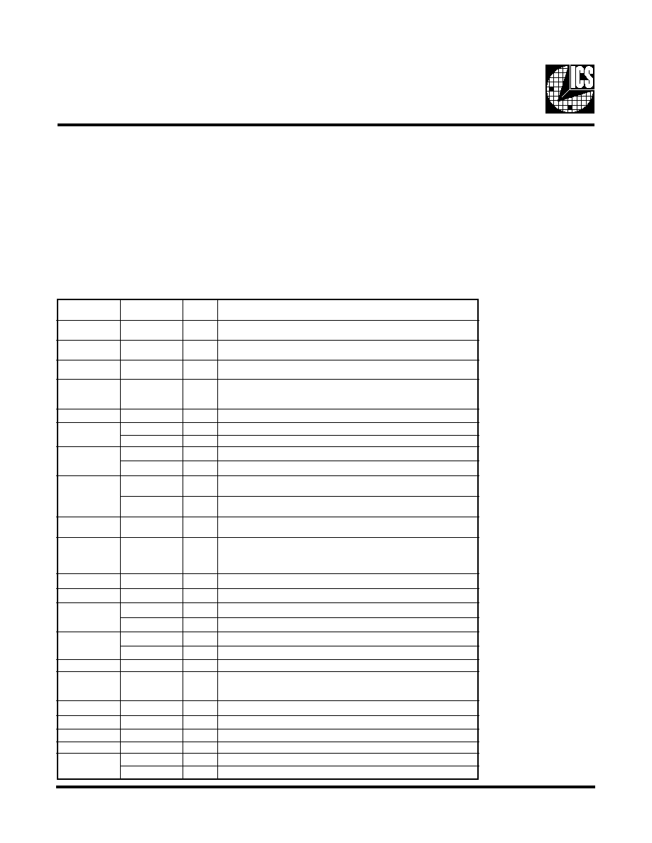
Register Name
Byte
Description
Pwd Default
Functionality & Frequency Select
Register
0
Output frequency, hardware / I
2
C frequency
select, spread spectrum & output enable
control register.
See individual byte
des cription
Output Control Registers
1-5
Active / inactive output control registers.
See individual byte
des cription
Byte Count Read Back Register
6
W riting to this register will configure byte
count and how many byte will be read back.
Do not write 00
H
to this byte.
06
H
Latched Inputs Read Back
Register
7
The inverse of the latched inputs level could
be read back from this register.
See individual byte
des cription
W atchdog Control Registers
8 Bit[6:0]
W atchdog enable, watchdog status and
programmable 'safe' frequency' can be
configured in this register.
000,0000
VCO Control Selection Bit
8 Bit[7]
This bit selects whether the output
frequency is controled by hardware/byte 0
configurations or byte 14&15 programming.
0
W atchdog Timer Count Register
9
W riting to this register will configure the
number of seconds for the watchdog timer
to reset.
FF
H
ICS Reserved Register
10
This is an unused register. W riting to this
register will not affect device functionality.
00
H
Device ID, Vendor ID & Revision ID
Registers
11-12
Byte 11 bit[3:0] is ICS vendor id - 0001.
Other bits in these 2 registers designate
device revision ID of this part.
See individual byte
des cription
ICS Reserved Register
13
Don't write into this register, writing 1's will
cause malfunction.
00
H
VCO Frequency Control Registers
14-15
These registers control the dividers ratio
into the phase detector and thus control the
VCO output frequency.
Depend on
hardware/byte 0
configuration
Spread Spectrum Control
Registers
16-17
These registers control the spread
percentage amount.
Depend on
hardware/byte 0
configuration
Output Dividers Control Registers
18-20
Changing bits in these registers result in
frequency divider ratio changes. Incorrect
configuration of group output divider ratio
can cause system malfunction.
Depend on
hardware/byte 0
configuration
Group Skews Control Registers
21-23
Increment or decrement the group skew
amount as compared to the initial skew.
See individual byte
des cription
Output Rise/Fall Time Select
Registers
24
These registers will control the group rise
and fall time.
See individual byte
des cription
Brief I
2
C registers description for ICS94201
Programmable System Frequency Generator