 | ÐлекÑÑоннÑй компоненÑ: ICS94210 | СкаÑаÑÑ:  PDF PDF  ZIP ZIP |
/home/web/doc/html/icst/173766
Integrated
Circuit
Systems, Inc.
ICS94210
Third party brands and names are the property of their respective owners.
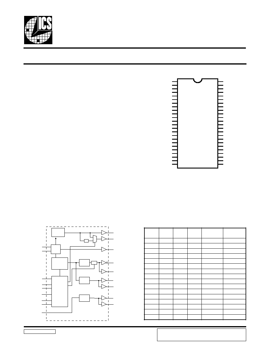
Block Diagram
94210 Rev A 10/10/00
Functionality
Pin Configuration
48-Pin 300mil SSOP
Recommended Application:
VIA KX133 style chipset
Output Features:
·
1 - Differential pair open drain CPU clocks
·
1 - Single-ended open drain CPU clock
·
13 - SDRAM @ 3.3V
·
6 - PCI @3.3V,
·
1 - 48MHz, @3.3V fixed.
·
1 - 24/48MHz @ 3.3V
·
2 - REF @3.3V, 14.318MHz.
Features:
·
Programmable ouput frequency.
·
Programmable ouput rise/fall time.
·
Programmable PCI_F and PCICLK skew.
·
Spread spectrum for EMI control typically
by 7dB to 8dB,
with programmable spread percentage.
·
Watchdog timer technology to reset system
if over-clocking causes malfunction.
·
Uses external 14.318MHz crystal.
·
FS pins for frequency select
Programmable System Clock Chip for AMD - K7 processor
* Internal Pull-up Resistor of 120K to VDD
VDD1
REF0/CPU_STOP#*
GND
X1
X2
VDD2
*MODE/PCICLK_F
*FS3/PCICLK0
GND
*SEL24_48#/PCICLK1
PCICLK2
PCICLK3
PCICLK4
VDD2
BUFFER IN
GND
SDRAM11
SDRAM10
VDD3
SDRAM9
SDRAM8
GND
SDATA
SCLK
REF1/FS2*
GND
CPUCLKT1
GND
CPUCLKC0
CPUCLKT0
VDD
PD#*
SDRAM_OUT
GND
SDRAM0
SDRAM1
VDD3
SDRAM2
SDRAM3
GND
SDRAM4
SDRAM5
VDD3
SDRAM6
SDRAM7
VDD4
48MHz/FS0*
24/48MHz/FS1*
ICS94210
1
2
3
4
5
6
7
8
9
10
11
12
13
14
15
16
17
18
19
20
21
22
23
24
48
47
46
45
44
43
42
41
40
39
38
37
36
35
34
33
32
31
30
29
28
27
26
25
SEL24_48#
BUFFER IN
PLL2
PLL1
Spread
Spectrum
48MHz
24_48MHz
SDRAM [11:0]
PCICLK [4:0]
PCICLK_F
SDRAM_OUT
CPUCLKT [0:1]
CPUCLKC0
X1
X2
XTAL
OSC
CPU
DIVDER
PCI
DIVDER
Stop
SDATA
SCLK
FS[3:0]
PD#
CPU_STOP#
Control
Logic
Config.
Reg.
/ 2
REF[0:1]
SDRAM
DRIVER
3
S
F
2
S
F
1
S
F
0
S
F
U
P
C
)
z
H
M
(
K
L
C
I
C
P
)
z
H
M
(
0
0
0
0
0
0
.
0
9
0
0
.
0
3
0
0
0
1
0
0
.
5
9
7
6
.
1
3
0
0
1
0
0
0
.
1
0
1
7
6
.
3
3
0
0
1
1
0
0
.
2
0
1
0
0
.
4
3
0
1
0
0
0
9
.
0
0
1
7
5
.
3
3
0
1
0
1
0
0
.
3
0
1
3
3
.
4
3
0
1
1
0
0
0
.
5
0
1
0
0
.
5
3
0
1
1
1
0
0
.
0
0
1
3
3
.
3
3
1
0
0
0
0
0
.
7
0
1
7
6
.
5
3
1
0
0
1
0
0
.
9
0
1
3
3
.
6
3
1
0
1
0
0
0
.
0
1
1
7
6
.
6
3
1
0
1
1
0
0
.
1
1
1
0
0
.
7
3
1
1
0
0
0
0
.
3
1
1
7
6
.
7
3
1
1
0
1
0
0
.
5
1
1
3
3
.
8
3
1
1
1
0
0
0
.
7
1
1
0
0
.
9
3
1
1
1
1
0
3
.
3
3
1
3
3
.
3
3
PRODUCT PREVIEW documents contain information on new
products in the sampling or preproduction phase of development.
Characteristic data and other specifications are subject to change
without notice.
Preliminary Product Preview
2
ICS94210
Preliminary Product Preview
Third party brands and names are the property of their respective owners.
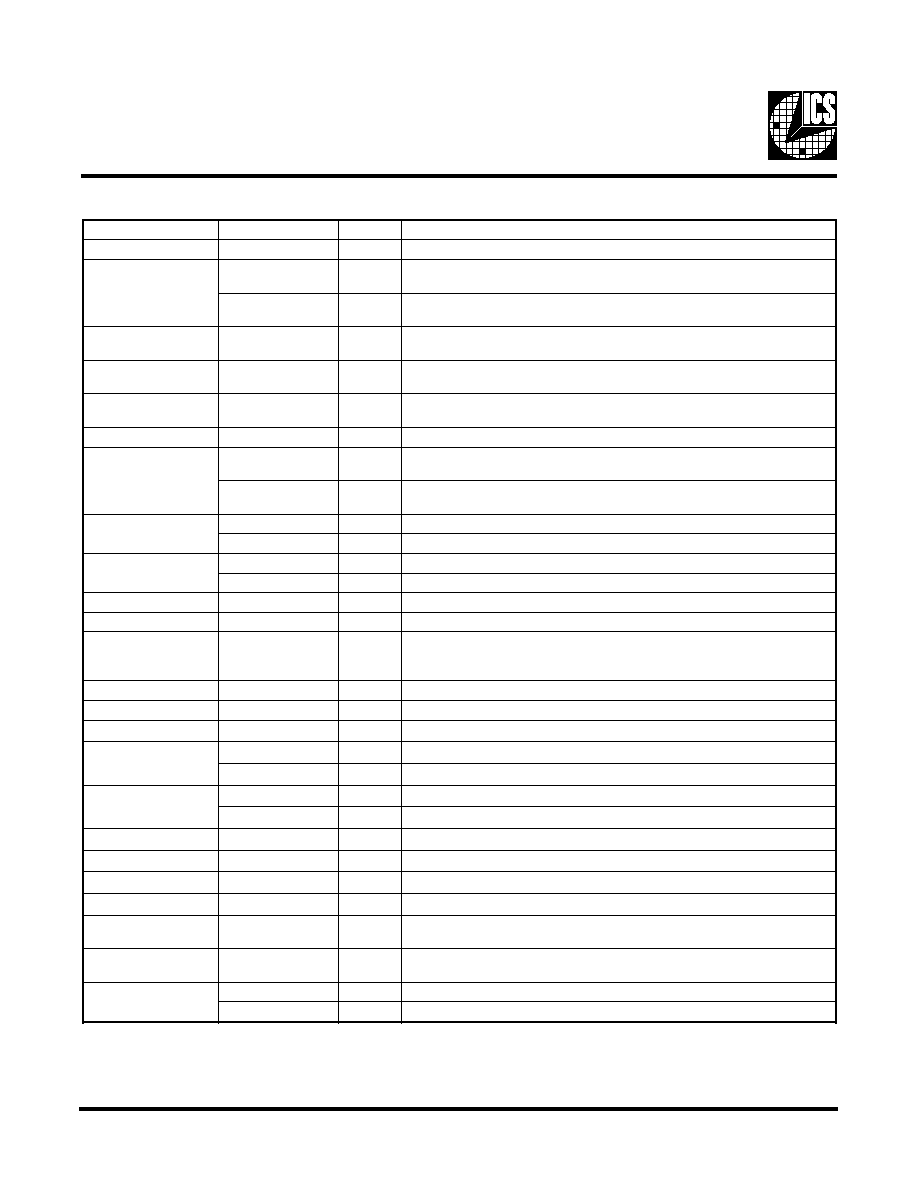
Pin Descriptions
Notes:
1:
Internal Pull-up Resistor of 120K to 3.3V on indicated inputs
2:
Bidirectional input/output pins, input logic levels are latched at internal power-on-reset. Use 10Kohm resistor
to program logic Hi to VDD or GND for logic low.
R
E
B
M
U
N
N
I
P
E
M
A
N
N
I
P
E
P
Y
T
N
O
I
T
P
I
R
C
S
E
D
1
1
D
D
V
R
W
P
V
3
.
3
l
a
n
i
m
o
n
,
y
l
p
p
u
s
r
e
w
o
p
L
A
T
X
,
)
2
:
0
(
f
e
R
2
0
F
E
R
T
U
O
R
E
G
N
O
R
T
S
e
h
t
s
i
t
u
p
t
u
o
F
E
R
s
i
h
T
.
k
c
o
l
c
e
c
n
e
r
e
f
e
r
z
h
M
8
1
3
.
4
1
s
d
a
o
l
S
U
B
A
S
I
r
o
f
r
e
f
f
u
b
#
P
O
T
S
_
U
P
C
2
,
1
N
I
"
0
"
c
i
g
o
l
t
a
&
C
K
L
C
U
P
C
,
T
K
L
C
U
P
C
s
t
l
a
h
t
u
p
n
i
s
u
o
n
o
r
h
c
n
y
s
a
s
i
h
T
.
w
o
l
n
e
v
i
r
d
n
e
h
w
l
e
v
e
l
,
2
2
,
6
1
,
9
,
3
7
4
,
5
4
,
9
3
,
3
3
D
N
G
R
W
P
d
n
u
o
r
G
4
1
X
N
I
k
c
a
b
d
e
e
f
d
n
a
)
F
p
6
3
(
p
a
c
d
a
o
l
l
a
n
r
e
t
n
i
s
a
h
,
t
u
p
n
i
l
a
t
s
y
r
C
2
X
m
o
r
f
r
o
t
s
i
s
e
r
5
2
X
T
U
O
d
a
o
l
l
a
n
r
e
t
n
i
s
a
H
.
z
H
M
8
1
3
.
4
1
y
l
l
a
n
i
m
o
n
,
t
u
p
t
u
o
l
a
t
s
y
r
C
)
F
p
6
3
(
p
a
c
4
1
,
6
2
D
D
V
R
W
P
V
3
.
3
l
a
n
i
m
o
n
,
)
4
:
0
(
K
L
C
I
C
P
d
n
a
F
_
K
L
C
I
C
P
r
o
f
y
l
p
p
u
S
7
F
_
K
L
C
I
C
P
T
U
O
r
e
w
o
p
r
o
f
#
P
O
T
S
_
I
C
P
y
b
d
e
t
c
e
f
f
a
t
o
n
k
c
o
l
c
I
C
P
g
n
i
n
n
u
r
e
e
r
F
.
t
n
e
m
e
g
a
n
a
m
E
D
O
M
2
,
1
N
I
e
l
i
b
o
M
=
0
,
e
d
o
M
p
o
t
k
s
e
D
=
1
,
n
i
p
t
c
e
l
e
s
n
o
i
t
c
n
u
f
8
1
n
i
p
,
7
1
n
i
P
.
t
u
p
n
I
d
e
h
c
t
a
L
.
e
d
o
M
8
3
S
F
2
,
1
N
I
D
N
G
o
t
n
w
o
d
-
l
l
u
P
l
a
n
r
e
t
n
I
.
t
u
p
n
I
d
e
h
c
t
a
L
.
n
i
p
t
c
e
l
e
s
y
c
n
e
u
q
e
r
F
0
K
L
C
I
C
P
T
U
O
t
u
p
t
u
o
k
c
o
l
c
I
C
P
0
1
#
8
4
_
4
2
L
E
S
2
,
1
N
I
t
u
p
t
u
o
5
2
n
i
p
r
o
f
z
H
M
8
4
r
o
4
2
t
c
e
l
e
s
o
t
t
u
p
n
i
c
i
g
o
L
1
K
L
C
I
C
P
T
U
O
.
t
u
p
t
u
o
k
c
o
l
c
I
C
P
3
1
,
2
1
,
1
1
)
4
:
2
(
K
L
C
I
C
P
T
U
O
.
s
t
u
p
t
u
o
k
c
o
l
c
I
C
P
5
1
N
I
R
E
F
F
U
B
N
I
.
s
t
u
p
t
u
o
M
A
R
D
S
r
o
f
s
r
e
f
f
u
B
t
u
o
n
a
F
o
t
t
u
p
n
I
,
1
2
,
0
2
,
8
1
,
7
1
,
2
3
,
1
3
,
9
2
,
8
2
8
3
,
7
3
,
5
3
,
4
3
)
0
:
1
1
(
M
A
R
D
S
T
U
O
n
i
p
N
I
R
E
F
F
U
B
m
o
r
f
s
t
u
p
t
u
o
r
e
f
f
u
B
t
u
o
n
a
F
,
s
t
u
p
t
u
o
k
c
o
l
c
M
A
R
D
S
.
)
t
e
s
p
i
h
c
y
b
d
e
l
l
o
r
t
n
o
c
(
6
3
,
0
3
,
9
1
3
D
D
V
R
W
P
.
V
3
.
3
l
a
n
i
m
o
n
)
2
1
:
0
(
M
A
R
D
S
r
o
f
y
l
p
p
u
S
3
2
A
T
A
D
S
N
I
I
r
o
f
t
u
p
n
i
a
t
a
D
2
t
u
p
n
i
t
n
a
r
e
l
o
t
V
5
,
t
u
p
n
i
l
a
i
r
e
s
C
4
2
K
L
C
S
N
I
I
f
o
t
u
p
n
i
k
c
o
l
C
2
t
u
p
n
i
t
n
a
r
e
l
o
t
V
5
,
t
u
p
n
i
C
5
2
z
H
M
8
4
_
4
2
T
U
O
t
u
p
t
u
o
k
c
o
l
c
z
H
M
8
4
/
z
H
M
4
2
1
S
F
2
,
1
N
I
.
t
u
p
n
I
d
e
h
c
t
a
L
.
n
i
p
t
c
e
l
e
s
y
c
n
e
u
q
e
r
F
6
2
z
H
M
8
4
T
U
O
k
c
o
l
c
t
u
p
t
u
o
z
H
M
8
4
0
S
F
2
,
1
N
I
t
u
p
n
I
d
e
h
c
t
a
L
.
n
i
p
t
c
e
l
e
s
y
c
n
e
u
q
e
r
F
7
2
4
D
D
V
R
W
P
.
e
r
o
c
L
L
P
d
e
x
i
f
d
n
a
s
r
e
f
f
u
b
t
u
p
t
u
o
z
H
M
8
4
&
4
2
r
o
f
r
e
w
o
P
0
4
T
U
O
_
M
A
R
D
S
T
U
O
r
e
f
f
u
b
y
a
l
e
d
o
r
e
z
M
A
R
D
S
r
o
f
k
c
o
l
c
e
c
n
e
r
e
f
e
R
1
4
#
D
P
2
,
1
N
I
w
o
l
e
v
i
t
c
a
,
p
i
h
c
n
w
o
d
s
r
e
w
o
P
2
4
D
D
V
R
W
P
V
3
.
3
e
r
o
c
r
o
f
y
l
p
p
u
S
6
4
,
3
4
)
1
:
0
(
T
K
L
C
U
P
C
T
U
O
n
i
a
r
d
n
e
p
o
e
s
e
h
T
.
s
t
u
p
t
u
o
U
P
C
r
i
a
p
l
a
i
t
n
e
r
e
f
f
i
d
f
o
s
k
c
o
l
c
"
e
u
r
T
"
.
p
u
-
l
l
u
p
V
5
.
1
l
a
n
r
e
t
x
e
n
a
d
e
e
n
s
t
u
p
t
u
o
4
4
0
C
K
L
C
U
P
C
T
U
O
e
s
e
h
T
.
s
t
u
p
t
u
o
U
P
C
r
i
a
p
l
a
i
t
n
e
r
e
f
f
i
d
f
o
s
k
c
o
l
c
"
y
r
o
t
n
e
m
e
l
p
m
o
C
"
.
p
u
-
l
l
u
p
V
5
.
1
l
a
n
r
e
t
x
e
n
a
d
e
e
n
s
t
u
p
t
u
o
n
i
a
r
d
n
e
p
o
8
4
1
F
E
R
T
U
O
.
k
c
o
l
c
e
c
n
e
r
e
f
e
r
z
H
M
8
1
3
.
4
1
2
S
F
2
,
1
N
I
t
u
p
n
I
d
e
h
c
t
a
L
.
n
i
p
t
c
e
l
e
s
y
c
n
e
u
q
e
r
F
3
ICS94210
Preliminary Product Preview
Third party brands and names are the property of their respective owners.
General Description
The ICS94210 is a main clock synthesizer chip for AMD-K7 based systems with VIA style chipset. This provides all clocks
required for such a system.
The ICS94210 belongs to ICS new generation of programmable system clock generators. It employs serial programming I
2
C
interface as a vehicle for changing output functions, changing output frequency, configuring output strength, configuring
output to output skew, changing spread spectrum amount, changing group divider ratio and dis/enabling individual clocks.
This device also has ICS propriety 'Watchdog Timer' technology which will reset the frequency to a safe setting if the system
become unstable from over clocking.
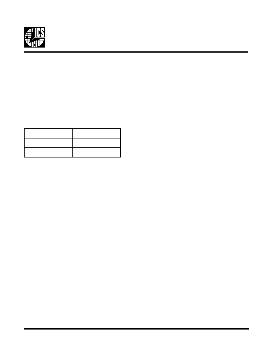
Mode Pin - Power Management Input Control
7
n
i
P
,
E
D
O
M
)
t
u
p
n
I
d
e
h
c
t
a
L
(
2
n
i
P
0
#
P
O
T
S
_
U
P
C
)
t
u
p
n
I
(
1
0
F
E
R
)
t
u
p
t
u
O
(
4
ICS94210
Preliminary Product Preview
Third party brands and names are the property of their respective owners.
General I
2
C serial interface information for the ICS94210
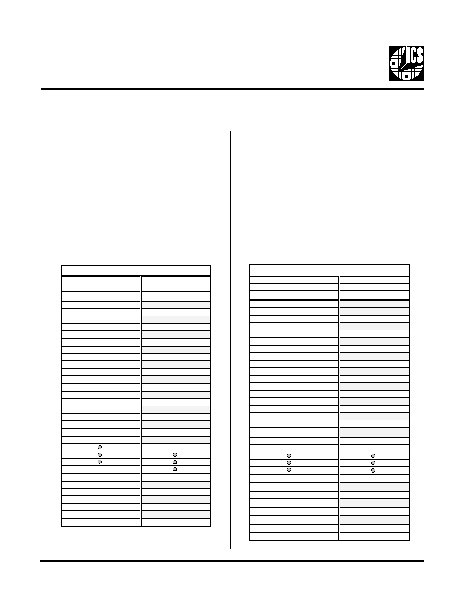
How to Write:
Controller (host) sends a start bit.
Controller (host) sends the write address D2
(H)
ICS clock will acknowledge
Controller (host) sends a dummy command code
ICS clock will acknowledge
Controller (host) sends a dummy byte count
ICS clock will acknowledge
Controller (host) starts sending Byte 0 through Byte 20
(see Note)
ICS clock will acknowledge each byte one at a time
Controller (host) sends a Stop bit
How to Read:
Controller (host) will send start bit.
Controller (host) sends the read address D3
(H)
ICS clock will acknowledge
ICS clock will send the byte count
Controller (host) acknowledges
ICS clock sends Byte 0 through byte 8 (default)
ICS clock sends Byte 0 through byte X (if X
(H)
was
written to byte 8).
Controller (host) will need to acknowledge each byte
Controller (host) will send a stop bit
*See notes on the following page
.
Controller (Host)
ICS (Slave/Receiver)
Start Bit
Address D2
(H)
ACK
Dummy Command Code
ACK
Dummy Byte Count
ACK
Byte 0
ACK
Byte 1
ACK
Byte 2
ACK
Byte 3
ACK
Byte 4
ACK
Byte 5
ACK
Byte 6
ACK
Byte 18
ACK
Byte 19
ACK
Byte 20
ACK
Stop Bit
How to Write:
Controller (Host)
ICS (Slave/Receiver)
Start Bit
Address D3
(H)
ACK
Byte Count
ACK
Byte 0
ACK
Byte 1
ACK
Byte 2
ACK
Byte 3
ACK
Byte 4
ACK
Byte 5
ACK
Byte 6
ACK
If 7
H
has been written to B6
Byte 7
ACK
If 12
H
has been written to B6
Byte18
ACK
If 13
H
has been written to B6
Byte 19
ACK
If 14
H
has been written to B6
Byte 20
ACK
Stop Bit
How to Read:
5
ICS94210
Preliminary Product Preview
Third party brands and names are the property of their respective owners.
1.
The ICS clock generator is a slave/receiver, I
2
C component. It can read back the data stored in the latches for
verification. Readback will support standard SMBUS controller protocol. The number of bytes to readback is
defined by writing to byte 8.
2.
When writing to byte 11 - 12, and byte 13 - 14, they must be written as a set. If for example, only byte 14 is written
but not 15, neither byte 14 or 15 will load into the receiver.
3.
The data transfer rate supported by this clock generator is 100K bits/sec or less (standard mode)
4.
The input is operating at 3.3V logic levels.
5.
The data byte format is 8 bit bytes.
6.
To simplify the clock generator I
2
C interface, the protocol is set to use only Block-Writes from the controller. The
bytes must be accessed in sequential order from lowest to highest byte with the ability to stop after any complete
byte has been transferred. The Command code and Byte count shown above must be sent, but the data is ignored
for those two bytes. The data is loaded until a Stop sequence is issued.
7.
At power-on, all registers are set to a default condition, as shown.
Notes:
Brief I
2
C registers description for ICS94210
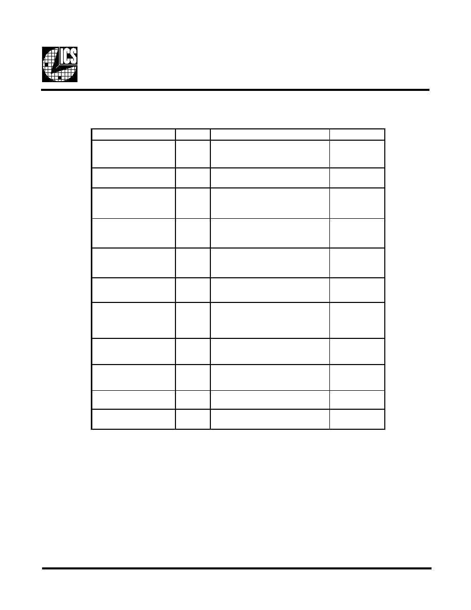
Programmable System Frequency Generator
R egister Name
Byte
Description
PWD Default
Functionality & Frequency
Select Register
0
O utput frequency, hardw are / I
2
C
frequency select, spread spectrum &
output enable control register.
See individual
byte description
Output Control Registers
1-6
A ctive / inactive output control
registers/latch inputs read back.
See individual
byte description
Vendor ID & Revision ID
Registers
7
Byte 11 bit[7:4] is ICS vendor id - 1001.
O ther bits in this register designate device
revision ID of this part.
See individual
byte description
Byte Count
Read Back Register
8
Writing to this register w ill configure
byte count and how many byte will be
read back. Do not w rite 00
H
to this byte.
08
H
Watchdog Timer
Count Register
9
Writing to this register w ill configure the
number of seconds for the watchdog
timer to reset.
10
H
Watchdog Control Registers 10 Bit [6:0]
Watchdog enable, w atchdog status and
programmable 'safe' frequency' can be
configured in this register.
000,0000
VCO Control Selection Bit
10 Bit [7]
This bit select whether the output
frequency is control by hardware/byte 0
configurations or byte 11&12
programming.
0
VCO Frequency Control
Registers
11-12
These registers control the dividers ratio
into the phase detector and thus control
the VCO output frequency.
Depended on
hardware/byte 0
configuration
Spread Spectrum Control
Registers
13-14
These registers control the spread
percentage amount.
Depended on
hardware/byte 0
configuration
Group Skew s Control
Registers
15-16
Increment or decrement the group skew
amount as compared to the initial skew.
See individual
byte description
Output Rise/Fall Time
Select Registers
17-20
These registers will control the output
rise and fall time.
See individual
byte description