Integrated
Circuit
Systems, Inc.
ICS950219
Preliminary Product Preview
0640C--05/28/03
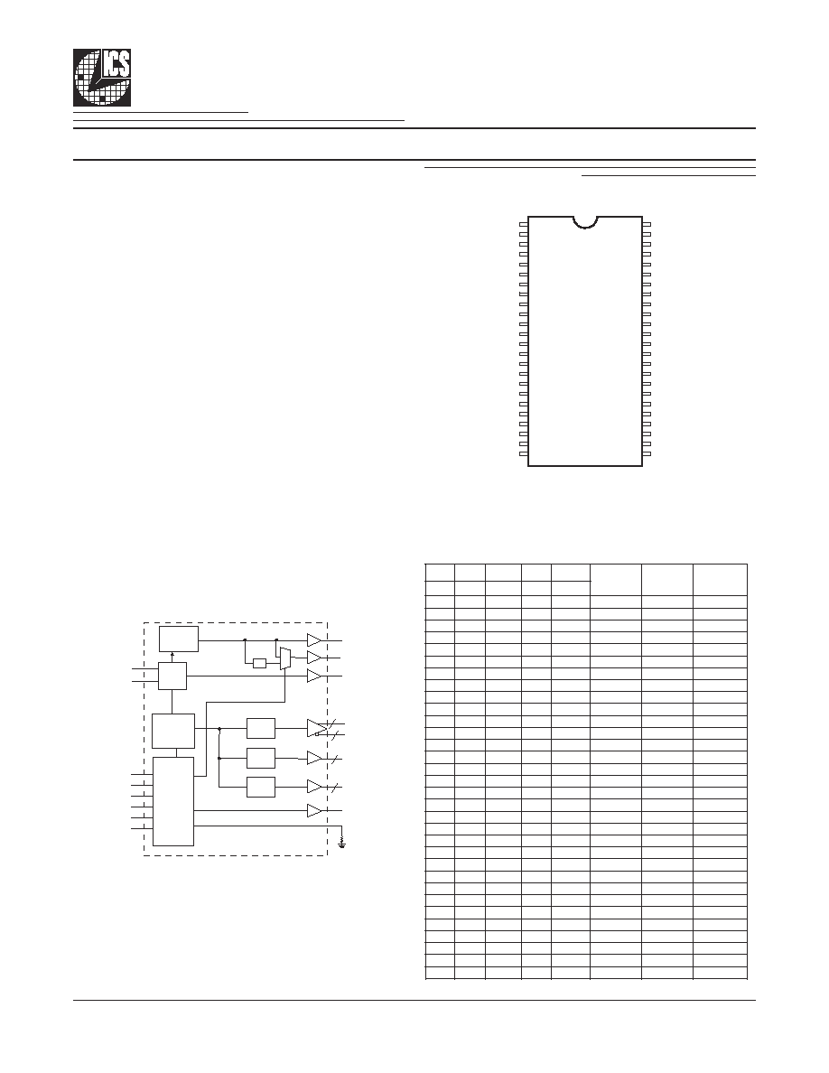
Block Diagram
Pin Configuration
Recommended Application:
CK-408 clock for IntelÆ 845 chipset with P4 processor.
Output Features:
∑
3 - Pairs of differential CPU clocks (differential current mode)
∑
4 - 3V66 @ 3.3V
∑
10 - PCI @ 3.3V
∑
1 - 48MHz @ 3.3V
∑
24-48 MHz selectable output @ 3.3V
∑
2 - REF @ 3.3V, 14.318MHz
Features/Benefits:
∑
Programmable output frequency.
∑
Programmable output divider ratios.
∑
Programmable output rise/fall time.
∑
Programmable output skew.
∑
Programmable spread percentage for EMI control.
∑
Watchdog timer technology to reset system
if system malfunctions.
∑
Programmable watch dog safe frequency.
∑
Support I
2
C Index read/write and block read/write operations.
∑
Uses external 14.318MHz crystal.
Key Specifications:
∑
CPU Output Jitter <150ps
∑
3V66 Output Jitter <250ps
∑
CPU Output Skew <100ps
Programmable Timing Control HubTM for P
4
TM
* Internal Pull-up resistor of 120K to VDD
48-Pin 300-mil SSOP
Frequency Table
2
t
i
B
7
t
i
B
6
t
i
B
5
t
i
B
4
t
i
B
K
L
C
U
P
C
z
H
M
6
6
V
3
z
H
M
K
L
C
I
C
P
z
H
M
4
S
F
3
S
F
2
S
F
1
S
F
0
S
F
0
0
0
0
0
0
0
.
2
0
1
0
0
.
8
6
0
0
.
4
3
0
0
0
0
1
0
0
.
5
0
1
0
0
.
0
7
0
0
.
5
3
0
0
0
1
0
0
0
.
8
0
1
0
0
.
2
7
0
0
.
6
3
0
0
0
1
1
0
0
.
1
1
1
0
0
.
4
7
0
0
.
7
3
0
0
1
0
0
0
0
.
4
1
1
0
0
.
6
7
0
0
.
8
3
0
0
1
0
1
0
0
.
7
1
1
0
0
.
8
7
0
0
.
9
3
0
0
1
1
0
0
0
.
0
2
1
0
0
.
0
8
0
0
.
0
4
0
0
1
1
1
0
0
.
3
2
1
0
0
.
2
8
0
0
.
1
4
0
1
0
0
0
0
0
.
6
2
1
0
0
.
2
7
0
0
.
6
3
0
1
0
0
1
0
0
.
0
3
1
0
3
.
4
7
0
1
.
7
3
0
1
0
1
0
0
0
.
6
3
1
0
0
.
8
6
0
0
.
4
3
0
1
0
1
1
0
0
.
0
4
1
0
0
.
0
7
0
0
.
5
3
0
1
1
0
0
0
0
.
4
4
1
0
0
.
2
7
0
0
.
6
3
0
1
1
0
1
0
0
.
8
4
1
0
0
.
4
7
0
0
.
7
3
0
1
1
1
0
0
0
.
2
5
1
0
0
.
6
7
0
0
.
8
3
0
1
1
1
1
0
0
.
6
5
1
0
0
.
8
7
0
0
.
9
3
1
0
0
0
0
0
0
.
0
6
1
0
0
.
0
8
0
0
.
0
4
1
0
0
0
1
0
0
.
4
6
1
0
0
.
2
8
0
0
.
1
4
1
0
0
1
0
6
6
.
6
6
1
6
6
.
6
6
3
3
.
3
3
1
0
0
1
1
0
0
.
0
7
1
0
0
.
8
6
0
0
.
4
3
1
0
1
0
0
0
0
.
5
7
1
0
0
.
0
7
0
0
.
5
3
1
0
1
0
1
0
0
.
0
8
1
0
0
.
2
7
0
0
.
6
3
1
0
1
1
0
0
0
.
5
8
1
0
0
.
4
7
0
0
.
7
3
1
0
1
1
1
0
0
.
0
9
1
0
0
.
6
7
0
0
.
8
3
1
1
0
0
0
0
8
.
6
6
0
8
.
6
6
0
4
.
3
3
1
1
0
0
1
0
2
.
0
0
1
0
8
.
6
6
0
4
.
3
3
1
1
0
1
0
0
6
.
3
3
1
0
8
.
6
6
0
4
.
3
3
1
1
0
1
1
0
4
.
0
0
2
0
8
.
6
6
0
4
.
3
3
1
1
1
0
0
6
6
.
6
6
6
6
.
6
6
3
3
.
3
3
1
1
1
0
1
0
0
.
0
0
1
6
6
.
6
6
3
3
.
3
3
1
1
1
1
0
0
0
.
0
0
2
6
6
.
6
6
3
3
.
3
3
1
1
1
1
1
3
3
.
3
3
1
6
6
.
6
6
3
3
.
3
3
*MULTISEL1/REF1
VDDREF
X1
X2
GND
*FS2/PCICLK0
*FS3/PCICLK1
PCICLK2
VDDPCI
*FS4/PCICLK3
PCICLK4
PCICLK5
GND
PCICLK6
PCICLK7
PCICLK8
PCICLK9
VDDPCI
Vtt_PWRGD#
RESET#
GND
*FS0/48MHz
*FS1/24_48MHz
AVDD48
REF0/MULTSEL0*
GND
VDDCPU
CPUCLKT2
CPUCLKC2
GND
PD#
CPUCLKT0
CPUCLKC0
VDDCPU
CPUCLKT1
CPUCLKC1
GND
I REF
AVDD
GND
VDD3V66
3V66_0
3V66_1
GND
3V66_2
3V66_3
SCLK
SDATA
ICS950219
1
2
3
4
5
6
7
8
9
10
11
12
13
14
15
16
17
18
19
20
21
22
23
24
48
47
46
45
44
43
42
41
40
39
38
37
36
35
34
33
32
31
30
29
28
27
26
25
PLL2
PLL1
Spread
Spectrum
PCICLK (9:0)
3V66 (3:0)
X1
X2
XTAL
OSC
CPU
DIVDER
PCI
DIVDER
3V66
DIVDER
PD#
MULTSEL(1:0)
SDATA
SCLK
Vtt_PWRGD#
FS (4:0)
I REF
RESET#
Control
Logic
Config.
Reg.
REF (1:0)
3
10
4
3
CPUCLKT (2:0)
CPUCLKC (2:0)
48MHz
24_48MHz
/ 2
PRODUCT PREVIEW documents contain information on new products in the sampling or preproduction phase of development. Characteristic data and other specifications are subject to change
without notice.

2
Integrated
Circuit
Systems, Inc.
ICS950219
Preliminary Product Preview
0640C--05/28/03
The ICS950219 is a single chip clock solution for desktop designs using the Intel 845 chipset with PC133 or DDR memory. It
provides all necessary clock signals for such a system.
The ICS950219 is part of a whole new line of ICS clock generators and buffers called TCHTM (Timing Control Hub). ICS is the first
to introduce a whole product line which offers full programmability and flexibility on a single clock device. This part incorporates ICS's
newest clock technology which offers more robust features and functionality. Employing the use of a serially programmable I
2
C
interface, this device can adjust the output clocks by configuring the frequency setting, the output divider ratios, selecting the ideal
spread percentage, the output skew, the output strength, and enabling/disabling each individual output clock. TCH also incorporates
ICS's Watchdog Timer technology and a reset feature to provide a safe setting under unstable system conditions. M/N control can
configure output frequency with resolution up to 0.1MHz increment. With all these programmable features ICS's, TCH makes mother
board testing, tuning and improvement very simple.
General Description
AVDD
GND
2
47
REF output, Crystal
24
21
48MHz fixed, Fixed PLL
39
43
CPU Outputs, CPU PLL, CPU Master
Clock,
VDD
GND
--
9, 18
5, 13
PCI outputs
32
29
3V66 outputs
46
36
CPU Outputs, IREF, MULTSEL
Pin Number
Description
Power Groups

3
Integrated
Circuit
Systems, Inc.
ICS950219
Preliminary Product Preview
0640C--05/28/03
Pin Description
R
E
B
M
U
N
N
I
P
E
M
A
N
N
I
P
E
P
Y
T
N
O
I
T
P
I
R
C
S
E
D
1
*
1
L
E
S
T
L
U
M
N
I
.
s
t
u
p
t
u
o
U
P
C
r
o
f
r
e
il
p
i
t
l
u
m
t
n
e
r
r
u
c
e
h
t
g
n
i
t
c
e
l
e
s
r
o
f
t
u
p
n
i
L
T
T
V
L
V
3
.
3
1
F
E
R
T
U
O
.
t
u
p
t
u
o
k
c
o
l
c
e
c
n
e
r
e
f
e
r
z
H
M
8
1
3
.
4
1
,
V
3
.
3
,
4
2
,
8
1
,
9
,
2
6
4
,
9
3
,
2
3
D
D
V
R
W
P
y
l
p
p
u
s
r
e
w
o
p
V
3
.
3
3
1
X
N
I
2
X
m
o
r
f
r
o
t
s
i
s
e
r
k
c
a
b
d
e
e
f
d
n
a
)
F
p
3
3
(
p
a
c
d
a
o
l
l
a
n
r
e
t
n
i
s
a
h
,
t
u
p
n
i
l
a
t
s
y
r
C
4
2
X
T
U
O
)
F
p
3
3
(
p
a
c
d
a
o
l
l
a
n
r
e
t
n
i
s
a
H
.
z
H
M
8
1
3
.
4
1
y
ll
a
n
i
m
o
n
,
t
u
p
t
u
o
l
a
t
s
y
r
C
,
9
2
,
1
2
,
3
1
,
5
7
4
,
3
4
,
6
3
D
N
G
R
W
P
y
l
p
p
u
s
V
3
.
3
r
o
f
s
n
i
p
d
n
u
o
r
G
6
2
S
F
*
N
I
.
n
o
r
e
w
o
p
t
a
d
e
h
c
t
a
l
t
u
p
n
I
.
t
i
b
t
c
e
l
e
s
y
c
n
e
u
q
e
r
f
t
u
p
n
i
c
i
g
o
L
0
K
L
C
I
C
P
T
U
O
t
u
p
t
u
o
k
c
o
l
c
I
C
P
V
3
.
3
7
3
S
F
*
N
I
.
n
o
r
e
w
o
p
t
a
d
e
h
c
t
a
l
t
u
p
n
I
.
t
i
b
t
c
e
l
e
s
y
c
n
e
u
q
e
r
f
t
u
p
n
i
c
i
g
o
L
1
K
L
C
I
C
P
T
U
O
t
u
p
t
u
o
k
c
o
l
c
I
C
P
V
3
.
3
0
1
4
S
F
*
N
I
.
n
o
r
e
w
o
p
t
a
d
e
h
c
t
a
l
t
u
p
n
I
.
t
i
b
t
c
e
l
e
s
y
c
n
e
u
q
e
r
f
t
u
p
n
i
c
i
g
o
L
3
K
L
C
I
C
P
T
U
O
t
u
p
t
u
o
k
c
o
l
c
I
C
P
V
3
.
3
,
2
1
,
4
1
,
5
1
,
6
1
,
7
1
8
,
1
1
)
2
,
4
:
9
(
K
L
C
I
C
P
T
U
O
s
t
u
p
t
u
o
k
c
o
l
c
I
C
P
V
3
.
3
9
1
#
D
G
R
W
P
_
t
t
V
N
I
S
F
n
e
h
w
e
n
i
m
r
e
t
e
d
o
t
d
e
s
u
e
b
o
r
t
s
e
v
i
t
i
s
n
e
s
l
e
v
e
l
a
s
i
t
u
p
n
i
L
T
T
V
L
t
n
a
r
e
l
o
t
V
5
s
i
h
T
d
e
l
p
m
a
s
e
b
o
t
y
d
a
e
r
e
r
a
d
n
a
d
il
a
v
e
r
a
s
t
u
p
n
i
L
E
S
I
T
L
U
M
d
n
a
)
0
:
4
(
)
w
o
l
e
v
i
t
c
a
(
0
2
#
T
E
S
E
R
T
U
O
.
t
u
o
e
m
i
t
r
e
m
m
i
t
g
o
d
h
c
t
a
w
r
o
e
u
l
a
v
y
c
n
e
u
q
e
r
f
r
o
f
l
a
n
g
i
s
t
e
s
e
r
m
e
t
s
y
s
e
m
i
t
l
a
e
R
.
w
o
l
e
v
i
t
c
a
s
i
l
a
n
g
i
s
s
i
h
T
1
3
,
0
3
,
8
2
,
7
2
)
0
:
3
(
6
6
V
3
T
U
O
B
U
H
r
o
f
s
t
u
p
t
u
o
k
c
o
l
c
z
H
M
6
6
d
e
x
i
F
V
3
.
3
2
2
0
S
F
*
N
I
.
n
o
r
e
w
o
p
t
a
d
e
h
c
t
a
l
t
u
p
n
I
.
t
i
b
t
c
e
l
e
s
y
c
n
e
u
q
e
r
f
t
u
p
n
i
c
i
g
o
L
z
H
M
8
4
T
U
O
.
t
u
p
t
u
o
k
c
o
l
c
z
H
M
8
4
d
e
x
i
F
V
3
.
3
3
2
1
S
F
*
N
I
.
n
o
r
e
w
o
p
t
a
d
e
h
c
t
a
l
t
u
p
n
I
.
t
i
b
t
c
e
l
e
s
y
c
n
e
u
q
e
r
f
t
u
p
n
i
c
i
g
o
L
z
H
M
8
4
_
4
2
T
U
O
t
u
p
t
u
o
z
H
M
8
4
r
o
4
2
e
l
b
a
t
c
e
l
e
S
5
2
A
T
A
D
S
O
/
I
I
r
o
f
n
i
p
a
t
a
D
2
t
n
a
r
e
l
o
t
V
5
y
r
t
i
u
c
r
i
c
C
6
2
K
L
C
S
N
I
I
r
o
f
n
i
p
k
c
o
l
C
2
t
n
a
r
e
l
o
t
V
5
y
r
t
i
u
c
r
i
c
C
3
3
D
N
G
R
W
P
L
L
P
E
R
O
C
r
o
f
d
n
u
o
r
G
4
3
D
D
V
A
R
W
P
l
a
n
i
m
o
n
V
3
.
3
L
L
P
E
R
O
C
r
o
f
r
e
w
o
P
5
3
F
E
R
I
T
U
O
n
i
p
s
i
h
T
.
s
r
i
a
p
K
L
C
U
P
C
e
h
t
r
o
f
t
n
e
r
r
u
c
e
c
n
e
r
e
f
e
r
e
h
t
s
e
h
s
il
b
a
t
s
e
n
i
p
s
i
h
T
e
h
t
h
s
il
b
a
t
s
e
o
t
r
e
d
r
o
n
i
d
n
u
o
r
g
o
t
d
e
i
t
r
o
t
s
i
s
e
r
n
o
i
s
i
c
e
r
p
d
e
x
i
f
a
s
e
r
i
u
q
e
r
.
t
n
e
r
r
u
c
e
t
a
i
r
p
o
r
p
p
a
2
4
#
D
P
N
I
w
o
l
a
o
t
n
i
e
c
i
v
e
d
e
h
t
n
w
o
d
r
e
w
o
p
o
t
d
e
s
u
n
i
p
t
u
p
n
i
w
o
l
e
v
i
t
c
a
s
u
o
n
o
r
h
c
n
y
s
A
e
r
a
l
a
t
s
y
r
c
e
h
t
d
n
a
O
C
V
e
h
t
d
n
a
d
e
l
b
a
s
i
d
e
r
a
s
k
c
o
l
c
l
a
n
r
e
t
n
i
e
h
T
.
e
t
a
t
s
r
e
w
o
p
.
s
m
3
n
a
h
t
r
e
t
a
e
r
g
e
b
t
o
n
ll
i
w
n
w
o
d
r
e
w
o
p
e
h
t
f
o
y
c
n
e
t
a
l
e
h
T
.
d
e
p
p
o
t
s
7
3
,
0
4
,
4
4
)
0
:
2
(
C
K
L
C
U
P
C
T
U
O
s
t
u
p
t
u
o
t
n
e
r
r
u
c
e
r
a
e
s
e
h
T
.
s
t
u
p
t
u
o
U
P
C
r
i
a
p
l
a
i
t
n
e
r
e
f
f
i
d
f
o
s
k
c
o
l
c
"
y
r
o
t
n
e
m
e
l
p
m
o
C
"
.
s
a
i
b
e
g
a
t
l
o
v
r
o
f
d
e
r
i
u
q
e
r
e
r
a
s
r
o
t
s
i
s
e
r
l
a
n
r
e
t
x
e
d
n
a
8
3
,
1
4
,
5
4
)
0
:
2
(
T
K
L
C
U
P
C
T
U
O
d
n
a
s
t
u
p
t
u
o
t
n
e
r
r
u
c
e
r
a
e
s
e
h
T
.
s
t
u
p
t
u
o
U
P
C
r
i
a
p
l
a
i
t
n
e
r
e
f
f
i
d
f
o
s
k
c
o
l
c
"
e
u
r
T
"
.
s
a
i
b
e
g
a
t
l
o
v
r
o
f
d
e
r
i
u
q
e
r
e
r
a
s
r
o
t
s
i
s
e
r
l
a
n
r
e
t
x
e
8
4
*
0
L
E
S
T
L
U
M
N
I
.
s
t
u
p
t
u
o
U
P
C
r
o
f
r
e
il
p
i
t
l
u
m
t
n
e
r
r
u
c
e
h
t
g
n
i
t
c
e
l
e
s
r
o
f
t
u
p
n
i
L
T
T
V
L
V
3
.
3
0
F
E
R
T
U
O
.
t
u
p
t
u
o
k
c
o
l
c
e
c
n
e
r
e
f
e
r
z
H
M
8
1
3
.
4
1
,
V
3
.
3
.
D
D
V
o
t
K
0
2
1
f
o
r
o
t
s
i
s
e
r
p
u
-
ll
u
p
l
a
n
r
e
t
n
I
*

4
Integrated
Circuit
Systems, Inc.
ICS950219
Preliminary Product Preview
0640C--05/28/03
Maximum Allowed Current
n
o
i
t
i
d
n
o
C
n
o
i
t
p
m
u
s
n
o
c
y
l
p
p
u
s
V
3
.
3
x
a
M
,
s
d
a
o
l
p
a
c
e
t
e
r
c
s
i
d
x
a
M
V
5
6
4
.
3
=
d
d
V
D
N
G
r
o
d
d
V
=
s
t
u
p
n
i
c
i
t
a
t
s
ll
A
e
d
o
M
n
w
o
d
r
e
w
o
P
)
0
=
#
N
W
D
R
W
P
(
A
m
0
4
e
v
i
t
c
A
l
l
u
F
A
m
0
6
3
0
L
E
S
T
L
U
M
1
L
E
S
T
L
U
M
t
e
g
r
a
T
d
r
a
o
B
Z
m
r
e
T
/
e
c
a
r
T
,
R
e
c
n
e
r
e
f
e
R
=
f
e
r
I
)
r
R
*
3
(
/
d
d
V
t
u
p
t
u
O
t
n
e
r
r
u
C
,
Z
@
h
o
V
A
m
2
3
.
2
=
f
e
r
I
0
0
s
m
h
o
0
6
%
1
5
7
4
=
r
R
A
m
2
3
.
2
=
f
e
r
I
f
e
r
I
*
5
=
h
o
I
0
6
@
V
1
7
.
0
0
0
s
m
h
o
0
5
%
1
5
7
4
=
r
R
A
m
2
3
.
2
=
f
e
r
I
f
e
r
I
*
5
=
h
o
I
0
5
@
V
9
5
.
0
0
1
s
m
h
o
0
6
%
1
5
7
4
=
r
R
A
m
2
3
.
2
=
f
e
r
I
f
e
r
I
*
6
=
h
o
I
0
6
2
/
V
5
8
.
0
0
1
s
m
h
o
0
5
%
1
5
7
4
=
r
R
A
m
2
3
.
2
=
f
e
r
I
f
e
r
I
*
6
=
h
o
I
0
5
@
V
1
7
.
0
1
0
s
m
h
o
0
6
%
1
5
7
4
=
r
R
A
m
2
3
.
2
=
f
e
r
I
f
e
r
I
*
4
=
h
o
I
0
6
@
V
6
5
.
0
1
0
s
m
h
o
0
5
%
1
5
7
4
=
r
R
A
m
2
3
.
2
=
f
e
r
I
f
e
r
I
*
4
=
h
o
I
0
5
@
V
7
4
.
0
1
1
s
m
h
o
0
6
%
1
5
7
4
=
r
R
A
m
2
3
.
2
=
f
e
r
I
f
e
r
I
*
7
=
h
o
I
0
6
@
V
9
9
.
0
1
1
s
m
h
o
0
5
%
1
5
7
4
=
r
R
A
m
2
3
.
2
=
f
e
r
I
f
e
r
I
*
7
=
h
o
I
0
5
@
V
2
8
.
0
0
0
)
v
i
u
q
e
C
D
(
0
3
%
1
1
2
2
=
r
R
A
m
5
=
f
e
r
I
f
e
r
I
*
5
=
h
o
I
0
3
@
V
5
7
.
0
0
0
)
v
i
u
q
e
C
D
(
5
2
%
1
1
2
2
=
r
R
A
m
5
=
f
e
r
I
f
e
r
I
*
5
=
h
o
I
0
2
@
V
2
6
.
0
0
1
)
v
i
u
q
e
C
D
(
0
3
%
1
1
2
2
=
r
R
A
m
5
=
f
e
r
I
f
e
r
I
*
6
=
h
o
I
0
3
@
V
0
9
.
0
0
1
)
v
i
u
q
e
C
D
(
5
2
%
1
1
2
2
=
r
R
A
m
5
=
f
e
r
I
f
e
r
I
*
6
=
h
o
I
0
2
@
V
5
7
.
0
1
0
)
v
i
u
q
e
C
D
(
0
3
%
1
1
2
2
=
r
R
A
m
5
=
f
e
r
I
f
e
r
I
*
4
=
h
o
I
0
2
@
0
6
.
0
1
0
)
v
i
u
q
e
C
D
(
5
2
%
1
1
2
2
=
r
R
A
m
5
=
f
e
r
I
f
e
r
I
*
4
=
h
o
I
0
2
@
V
5
.
0
1
1
)
v
i
u
q
e
C
D
(
0
3
%
1
1
2
2
=
r
R
A
m
5
=
f
e
r
I
f
e
r
I
*
7
=
h
o
I
0
3
@
V
5
0
.
1
1
1
)
v
i
u
q
e
C
D
(
5
2
%
1
1
2
2
=
r
R
A
m
5
=
f
e
r
I
f
e
r
I
*
7
=
h
o
I
0
2
@
V
4
8
.
0
CPUCLK Swing Select Functions

5
Integrated
Circuit
Systems, Inc.
ICS950219
Preliminary Product Preview
0640C--05/28/03
General I
2
C serial interface information
How to Write:
∑
Controller (host) sends a start bit.
∑ Controller (host) sends the write address D2
(H)
∑ ICS clock will
acknowledge
∑ Controller (host) sends the begining byte location = N
∑ ICS clock will
acknowledge
∑ Controller (host) sends the data byte count = X
∑ ICS clock will
acknowledge
∑ Controller (host) starts sending
Byte N through
Byte N + X -1
(see Note 2)
∑ ICS clock will
acknowledge each byte one at a time
∑ Controller (host) sends a Stop bit
How to Read:
∑ Controller (host) will send start bit.
∑ Controller (host) sends the write address D2
(H)
∑ ICS clock will
acknowledge
∑ Controller (host) sends the begining byte
location = N
∑ ICS clock will
acknowledge
∑ Controller (host) will send a separate start bit.
∑ Controller (host) sends the read address D3
(H)
∑ ICS clock will
acknowledge
∑ ICS clock will send the data byte count = X
∑ ICS clock sends
Byte N + X -1
∑ ICS clock sends
Byte 0 through byte X (if X
(H)
was written to byte 8)
.
∑ Controller (host) will need to acknowledge each byte
∑ Controllor (host) will send a not acknowledge bit
∑ Controller (host) will send a stop bit
*See notes on the following page
.
ICS (Slave/Receiver)
T
WR
ACK
ACK
ACK
ACK
ACK
P
stoP bit
X Byt
e
Index Block Write Operation
Slave Address D2
(H)
Beginning Byte = N
WRite
starT bit
Controller (Host)
Byte N + X - 1
Data Byte Count = X
Beginning Byte N
T
starT bit
WR
WRite
RT
Repeat starT
RD
ReaD
Beginning Byte N
Byte N + X - 1
N
Not acknowledge
P
stoP bit
Slave Address D3
(H)
Index Block Read Operation
Slave Address D2
(H)
Beginning Byte = N
ACK
ACK
Data Byte Count = X
ACK
ICS (Slave/Receiver)
Controller (Host)
X Byt
e
ACK
ACK

6
Integrated
Circuit
Systems, Inc.
ICS950219
Preliminary Product Preview
0640C--05/28/03
Byte 0: Functionality and frequency select register (Default=0)
Notes:
1. Default at power-up will be for latched logic inputs to define frequency, as displayed by Bit 3.
t
i
B
n
o
i
t
p
i
r
c
s
e
D
D
W
P
t
i
B
)
4
:
7
,
2
(
2
t
i
B
7
t
i
B
6
t
i
B
5
t
i
B
4
t
i
B
K
L
C
U
P
C
z
H
M
6
6
V
3
z
H
M
K
L
C
I
C
P
z
H
M
%
d
a
e
r
p
S
1
e
t
o
N
4
S
F
3
S
F
2
S
F
1
S
F
0
S
F
0
0
0
0
0
0
0
.
2
0
1
0
0
.
8
6
0
0
.
4
3
d
a
e
r
p
s
r
e
t
n
e
C
%
5
2
.
0
-
/
+
0
0
0
0
1
0
0
.
5
0
1
0
0
.
0
7
0
0
.
5
3
d
a
e
r
p
s
r
e
t
n
e
C
%
5
2
.
0
-
/
+
0
0
0
1
0
0
0
.
8
0
1
0
0
.
2
7
0
0
.
6
3
d
a
e
r
p
s
r
e
t
n
e
C
%
5
2
.
0
-
/
+
0
0
0
1
1
0
0
.
1
1
1
0
0
.
4
7
0
0
.
7
3
d
a
e
r
p
s
r
e
t
n
e
C
%
5
2
.
0
-
/
+
0
0
1
0
0
0
0
.
4
1
1
0
0
.
6
7
0
0
.
8
3
d
a
e
r
p
s
r
e
t
n
e
C
%
5
2
.
0
-
/
+
0
0
1
0
1
0
0
.
7
1
1
0
0
.
8
7
0
0
.
9
3
d
a
e
r
p
s
r
e
t
n
e
C
%
5
2
.
0
-
/
+
0
0
1
1
0
0
0
.
0
2
1
0
0
.
0
8
0
0
.
0
4
d
a
e
r
p
s
r
e
t
n
e
C
%
5
2
.
0
-
/
+
0
0
1
1
1
0
0
.
3
2
1
0
0
.
2
8
0
0
.
1
4
d
a
e
r
p
s
r
e
t
n
e
C
%
5
2
.
0
-
/
+
0
1
0
0
0
0
0
.
6
2
1
0
0
.
2
7
0
0
.
6
3
d
a
e
r
p
s
r
e
t
n
e
C
%
5
2
.
0
-
/
+
0
1
0
0
1
0
0
.
0
3
1
0
3
.
4
7
0
1
.
7
3
d
a
e
r
p
s
r
e
t
n
e
C
%
5
2
.
0
-
/
+
0
1
0
1
0
0
0
.
6
3
1
0
0
.
8
6
0
0
.
4
3
d
a
e
r
p
s
r
e
t
n
e
C
%
5
2
.
0
-
/
+
0
1
0
1
1
0
0
.
0
4
1
0
0
.
0
7
0
0
.
5
3
d
a
e
r
p
s
r
e
t
n
e
C
%
5
2
.
0
-
/
+
0
1
1
0
0
0
0
.
4
4
1
0
0
.
2
7
0
0
.
6
3
d
a
e
r
p
s
r
e
t
n
e
C
%
5
2
.
0
-
/
+
0
1
1
0
1
0
0
.
8
4
1
0
0
.
4
7
0
0
.
7
3
d
a
e
r
p
s
r
e
t
n
e
C
%
5
2
.
0
-
/
+
0
1
1
1
0
0
0
.
2
5
1
0
0
.
6
7
0
0
.
8
3
d
a
e
r
p
s
r
e
t
n
e
C
%
5
2
.
0
-
/
+
0
1
1
1
1
0
0
.
6
5
1
0
0
.
8
7
0
0
.
9
3
d
a
e
r
p
s
r
e
t
n
e
C
%
5
2
.
0
-
/
+
1
0
0
0
0
0
0
.
0
6
1
0
0
.
0
8
0
0
.
0
4
d
a
e
r
p
s
r
e
t
n
e
C
%
5
2
.
0
-
/
+
1
0
0
0
1
0
0
.
4
6
1
0
0
.
2
8
0
0
.
1
4
d
a
e
r
p
s
r
e
t
n
e
C
%
5
2
.
0
-
/
+
1
0
0
1
0
0
6
.
6
6
1
6
6
.
6
6
3
3
.
3
3
d
a
e
r
p
s
r
e
t
n
e
C
%
5
2
.
0
-
/
+
1
0
0
1
1
0
0
.
0
7
1
0
0
.
8
6
0
0
.
4
3
d
a
e
r
p
s
r
e
t
n
e
C
%
5
2
.
0
-
/
+
1
0
1
0
0
0
0
.
5
7
1
0
0
.
0
7
0
0
.
5
3
d
a
e
r
p
s
r
e
t
n
e
C
%
5
2
.
0
-
/
+
1
0
1
0
1
0
0
.
0
8
1
0
0
.
2
7
0
0
.
6
3
d
a
e
r
p
s
r
e
t
n
e
C
%
5
2
.
0
-
/
+
1
0
1
1
0
0
0
.
5
8
1
0
0
.
4
7
0
0
.
7
3
d
a
e
r
p
s
r
e
t
n
e
C
%
5
2
.
0
-
/
+
1
0
1
1
1
0
0
.
0
9
1
0
0
.
6
7
0
0
.
8
3
d
a
e
r
p
s
r
e
t
n
e
C
%
5
2
.
0
-
/
+
1
1
0
0
0
0
8
.
6
6
0
8
.
6
6
0
4
.
3
3
d
a
e
r
p
s
r
e
t
n
e
C
%
5
2
.
0
-
/
+
1
1
0
0
1
0
2
.
0
0
1
0
8
.
6
6
0
4
.
3
3
d
a
e
r
p
s
r
e
t
n
e
C
%
5
2
.
0
-
/
+
1
1
0
1
0
0
6
.
3
3
1
0
8
.
6
6
0
4
.
3
3
d
a
e
r
p
s
r
e
t
n
e
C
%
5
2
.
0
-
/
+
1
1
0
1
1
0
4
.
0
0
2
0
8
.
6
6
0
4
.
3
3
d
a
e
r
p
s
r
e
t
n
e
C
%
5
2
.
0
-
/
+
1
1
1
0
0
6
6
.
6
6
6
6
.
6
6
3
3
.
3
3
d
a
e
r
p
s
n
w
o
D
%
6
.
0
-
o
t
0
1
1
1
0
1
0
0
.
0
0
1
6
6
.
6
6
3
3
.
3
3
d
a
e
r
p
s
n
w
o
D
%
6
.
0
-
o
t
0
1
1
1
1
0
0
0
.
0
0
2
6
6
.
6
6
3
3
.
3
3
d
a
e
r
p
s
n
w
o
D
%
6
.
0
-
o
t
0
1
1
1
1
1
3
3
.
3
3
1
6
6
.
6
6
3
3
.
3
3
d
a
e
r
p
s
n
w
o
D
%
6
.
0
-
o
t
0
3
t
i
B
s
t
u
p
n
i
d
e
h
c
t
a
l
,
t
c
e
l
e
s
e
r
a
w
d
r
a
h
y
b
d
e
t
c
e
l
e
s
s
i
y
c
n
e
u
q
e
r
F
-
0
4
:
7
,
2
t
i
B
y
b
d
e
t
c
e
l
e
s
s
i
y
c
n
e
u
q
e
r
F
-
1
0
1
t
i
B
l
a
m
r
o
N
-
0
e
l
b
a
n
e
m
u
r
t
c
e
p
s
d
a
e
r
p
S
-
1
0
0
t
i
B
s
t
u
p
n
i
h
c
t
a
l
y
b
d
e
t
c
e
l
e
s
e
b
l
l
i
w
y
c
n
e
u
q
e
r
f
e
f
a
s
g
o
d
h
c
t
a
W
-
0
)
0
:
4
(
t
i
b
0
1
e
t
y
B
y
b
d
e
m
m
a
r
g
o
r
p
e
b
l
l
i
w
y
c
n
e
u
q
e
r
f
e
f
a
s
g
o
d
h
c
t
a
W
-
1
0
7
Integrated
Circuit
Systems, Inc.
ICS950219
Preliminary Product Preview
0640C--05/28/03
Byte 1: Output Control Register
(1 = enable, 0 = disable)
Byte 3: Output Control Register
(1 = enable, 0 = disable)
Byte 2: Output Control Register
(1 = enable, 0 = disable)
Byte 4: Output Control Register
(1 = enable, 0 = disable)
t
i
B
#
n
i
P
D
W
P
n
o
i
t
p
i
r
c
s
e
D
7
t
i
B
4
4
,
5
4
1
2
C
/
T
U
P
C
6
t
i
B
7
3
,
8
3
1
1
C
/
T
U
P
C
5
t
i
B
0
4
,
1
4
1
0
C
/
T
U
P
C
4
t
i
B
-
X
k
c
a
b
d
a
e
R
4
S
F
3
t
i
B
-
X
k
c
a
b
d
a
e
R
3
S
F
2
t
i
B
-
X
k
c
a
b
d
a
e
R
2
S
F
1
t
i
B
-
X
k
c
a
b
d
a
e
R
1
S
F
0
t
i
B
-
X
k
c
a
b
d
a
e
R
0
S
F
t
i
B
#
n
i
P
D
W
P
n
o
i
t
p
i
r
c
s
e
D
7
t
i
B
-
1
d
e
v
r
e
s
e
R
6
t
i
B
7
1
1
9
_
K
L
C
I
C
P
5
t
i
B
6
1
1
8
_
K
L
C
I
C
P
4
t
i
B
5
1
1
7
_
K
L
C
I
C
P
3
t
i
B
4
1
1
6
_
K
L
C
I
C
P
2
t
i
B
2
1
1
5
_
K
L
C
I
C
P
1
t
i
B
1
1
1
4
_
K
L
C
I
C
P
0
t
i
B
0
1
1
3
_
K
L
C
I
C
P
t
i
B
#
n
i
P
D
W
P
n
o
i
t
p
i
r
c
s
e
D
7
t
i
B
-
X
)
k
c
a
b
d
a
e
r
(
0
L
E
S
i
t
l
u
M
6
t
i
B
-
X
)
k
c
a
b
d
a
e
R
(
1
L
E
S
i
t
l
u
M
5
t
i
B
1
3
1
0
-
6
6
V
3
4
t
i
B
0
3
1
1
-
6
6
V
3
3
t
i
B
8
4
1
0
F
E
R
2
t
i
B
1
1
1
F
E
R
1
t
i
B
7
2
1
3
_
6
6
V
3
0
t
i
B
8
2
1
2
_
6
6
V
3
Notes:
1. PWD = Power on Default
2. For disabled clocks, they stop low for single ended clocks. Differential CPU clocks stop with CPUCLKT at high,
CPUCLKC off, and external resistor termination will bring CPUCLKC low.
t
i
B
#
n
i
P
D
W
P
n
o
i
t
p
i
r
c
s
e
D
7
t
i
B
3
2
1
1
_
z
H
M
8
4
6
t
i
B
2
2
1
0
_
z
H
M
8
4
5
t
i
B
-
1
e
l
b
a
s
i
D
=
0
,
e
l
b
a
n
E
=
1
t
c
e
t
e
d
t
f
i
h
s
r
a
e
g
t
e
s
e
R
4
t
i
B
-
X
d
e
v
r
e
s
e
R
3
t
i
B
-
0
z
H
M
8
4
=
1
,
z
H
M
4
2
=
0
;
z
H
M
8
4
_
4
2
l
e
S
2
t
i
B
8
1
2
_
K
L
C
I
C
P
1
t
i
B
7
1
1
_
K
L
C
I
C
P
0
t
i
B
6
1
0
_
K
L
C
I
C
P

8
Integrated
Circuit
Systems, Inc.
ICS950219
Preliminary Product Preview
0640C--05/28/03
Byte 7: Revision ID and Device ID Register
Byte 8: Byte Count Read Back Register
Byte 5: Programming Edge Rate
(1 = enable, 0 = disable)
Byte 6: Vendor ID Register
(1 = enable, 0 = disable)
t
i
B
e
m
a
N
D
W
P
n
o
i
t
p
i
r
c
s
e
D
7
t
i
B
7
e
t
y
B
0
w
o
h
d
n
a
t
n
u
o
c
e
t
y
b
e
r
u
g
i
f
n
o
c
ll
i
w
r
e
t
s
i
g
e
r
s
i
h
t
o
t
g
n
i
t
i
r
W
:
e
t
o
N
s
i
t
l
u
a
f
e
d
,
k
c
a
b
d
a
e
r
e
b
ll
i
w
s
e
t
y
b
y
n
a
m
F
0
H
.
s
e
t
y
b
5
1
=
6
t
i
B
6
e
t
y
B
0
5
t
i
B
5
e
t
y
B
0
4
t
i
B
4
e
t
y
B
0
3
t
i
B
3
e
t
y
B
1
2
t
i
B
2
e
t
y
B
1
1
t
i
B
1
e
t
y
B
1
0
t
i
B
0
e
t
y
B
1
t
i
B
e
m
a
N
D
W
P
n
o
i
t
p
i
r
c
s
e
D
7
t
i
B
7
D
I
e
c
i
v
e
D
0
e
c
i
v
e
d
l
a
u
d
i
v
i
d
n
i
n
o
d
e
s
a
b
e
b
ll
i
w
s
e
u
l
a
v
D
I
e
c
i
v
e
D
.
e
s
a
c
s
i
h
t
n
i
"
H
8
2
"
6
t
i
B
6
D
I
e
c
i
v
e
D
0
5
t
i
B
5
D
I
e
c
i
v
e
D
1
4
t
i
B
4
D
I
e
c
i
v
e
D
0
3
t
i
B
3
D
I
e
c
i
v
e
D
1
2
t
i
B
2
D
I
e
c
i
v
e
D
0
1
t
i
B
1
D
I
e
c
i
v
e
D
0
0
t
i
B
0
D
I
e
c
i
v
e
D
0
t
i
B
e
m
a
N
D
W
P
n
o
i
t
p
i
r
c
s
e
D
7
t
i
B
3
t
i
B
D
I
n
o
i
s
i
v
e
R
X
n
o
i
s
i
v
e
r
s
'
e
c
i
v
e
d
l
a
u
d
i
v
i
d
n
i
n
o
d
e
s
a
b
e
b
ll
i
w
s
e
u
l
a
v
D
I
n
o
i
s
i
v
e
R
6
t
i
B
2
t
i
B
D
I
n
o
i
s
i
v
e
R
X
5
t
i
B
1
t
i
B
D
I
n
o
i
s
i
v
e
R
X
4
t
i
B
0
t
i
B
D
I
n
o
i
s
i
v
e
R
X
3
t
i
B
3
t
i
B
D
I
r
o
d
n
e
V
0
)
d
e
v
r
e
s
e
R
(
2
t
i
B
2
t
i
B
D
I
r
o
d
n
e
V
0
)
d
e
v
r
e
s
e
R
(
1
t
i
B
1
t
i
B
D
I
r
o
d
n
e
V
0
)
d
e
v
r
e
s
e
R
(
0
t
i
B
0
t
i
B
D
I
r
o
d
n
e
V
1
)
d
e
v
r
e
s
e
R
(
t
i
B
#
n
i
P
D
W
P
n
o
i
t
p
i
r
c
s
e
D
7
t
i
B
-
1
)
d
e
v
r
e
s
e
R
(
6
t
i
B
X
1
)
d
e
v
r
e
s
e
R
(
5
t
i
B
X
1
)
d
e
v
r
e
s
e
R
(
4
t
i
B
X
1
)
d
e
v
r
e
s
e
R
(
3
t
i
B
X
1
)
d
e
v
r
e
s
e
R
(
2
t
i
B
X
1
)
d
e
v
r
e
s
e
R
(
1
t
i
B
X
1
1
t
i
b
l
o
r
t
n
o
c
I
C
P
/
6
6
V
3
.
c
n
y
s
A
0
t
i
B
X
0
0
t
i
b
l
o
r
t
n
o
c
I
C
P
/
6
6
V
3
.
c
n
y
s
A
1
t
i
b
5
B
0
1
0
=
0
t
i
b
5
B
)
U
P
C
h
t
i
w
c
n
y
s
A
(
z
H
M
0
0
.
3
3
/
z
H
M
1
0
.
6
6
)
U
P
C
h
t
i
w
c
n
y
S
(
z
H
M
3
3
.
3
3
/
z
H
M
6
6
.
6
6
1
=
0
t
i
b
5
B
)
U
P
C
h
t
i
w
c
n
y
s
A
(
z
H
M
2
7
.
7
3
/
z
H
M
4
4
.
5
7
)
U
P
C
h
t
i
w
c
n
y
s
A
(
z
H
M
1
0
.
4
4
/
z
H
M
1
0
.
8
8
Asynchronous 3V66/PCI Frequency Selection Table
9
Integrated
Circuit
Systems, Inc.
ICS950219
Preliminary Product Preview
0640C--05/28/03
Byte 10: Programming Enable bit 8 Watchdog Control Register
Byte 11: VCO Frequency M Divider (Reference divider) Control Register
Byte 12: VCO Frequency N Divider (VCO divider) Control Register
Byte 9: Watchdog Timer Count Register
t
i
B
e
m
a
N
D
W
P
n
o
i
t
p
i
r
c
s
e
D
7
t
i
B
7
D
W
0
∑
X
o
t
d
n
o
p
s
e
r
r
o
c
s
t
i
b
8
e
s
e
h
t
f
o
n
o
i
t
a
t
n
e
s
e
r
p
e
r
l
a
m
i
c
e
d
e
h
T
e
d
o
m
m
r
a
l
a
o
t
s
e
o
g
t
i
e
r
o
f
e
b
t
i
a
w
ll
i
w
r
e
m
i
t
g
o
d
h
c
t
a
w
e
h
t
s
m
0
9
2
s
i
p
u
r
e
w
o
p
t
a
t
l
u
a
f
e
D
.
g
n
i
t
t
e
s
e
f
a
s
e
h
t
o
t
y
c
n
e
u
q
e
r
f
e
h
t
t
e
s
e
r
d
n
a
.
s
d
n
o
c
e
s
3
.
2
=
s
m
0
9
2
∑
8
6
t
i
B
6
D
W
0
5
t
i
B
5
D
W
0
4
t
i
B
4
D
W
0
3
t
i
B
3
D
W
1
2
t
i
B
2
D
W
0
1
t
i
B
1
D
W
0
0
t
i
B
0
D
W
0
t
i
B
e
m
a
N
D
W
P
n
o
i
t
p
i
r
c
s
e
D
7
t
i
B
8
v
i
d
N
X
8
t
i
b
r
e
d
i
v
i
d
N
6
t
i
B
6
v
i
d
M
X
e
h
t
o
t
d
s
o
p
s
e
r
r
o
c
)
0
:
6
(
v
i
d
M
f
o
n
o
i
t
a
t
n
e
s
e
r
p
s
e
r
l
a
m
i
c
e
d
e
h
T
e
h
t
o
t
l
a
u
q
e
s
i
p
u
r
e
w
o
p
t
a
t
l
u
a
f
e
D
.
e
u
l
a
v
r
e
d
i
v
i
d
e
c
n
e
r
e
f
e
r
.
n
o
i
t
c
e
l
e
s
s
t
u
p
n
i
d
e
h
c
t
a
l
5
t
i
B
5
v
i
d
M
X
4
t
i
B
4
v
i
d
M
X
3
t
i
B
3
v
i
d
M
X
2
t
i
B
2
v
i
d
M
X
1
t
i
B
1
v
i
d
M
X
0
t
i
B
0
v
i
d
M
X
t
i
B
e
m
a
N
D
W
P
n
o
i
t
p
i
r
c
s
e
D
7
t
i
B
7
v
i
d
N
X
e
h
t
o
t
d
n
o
p
s
e
r
r
o
c
)
0
:
8
(
v
i
d
N
f
o
n
o
i
t
a
t
n
e
s
e
r
p
e
r
l
a
m
i
c
e
d
e
h
T
e
h
t
o
t
l
a
u
q
e
s
i
p
u
r
e
w
o
p
t
a
t
l
u
a
f
e
D
.
e
u
l
a
v
r
e
d
i
v
i
d
O
C
V
.
1
1
e
t
y
B
n
i
d
e
t
a
c
o
l
s
i
8
v
i
d
N
e
c
i
t
o
N
.
n
o
t
c
e
l
e
s
s
t
u
p
n
i
d
e
h
c
t
a
l
6
t
i
B
6
v
i
d
N
X
5
t
i
B
5
v
i
d
N
X
4
t
i
B
4
v
i
d
N
X
3
t
i
B
3
v
i
d
N
X
2
t
i
B
2
v
i
d
N
X
1
t
i
B
1
v
i
d
N
X
0
t
i
B
0
v
i
d
N
X
t
i
B
e
m
a
N
D
W
P
n
o
i
t
p
i
r
c
s
e
D
7
t
i
B
m
a
r
g
o
r
P
e
l
b
a
n
E
0
t
i
b
e
l
b
a
n
E
g
n
i
m
m
a
r
g
o
r
P
1
0
e
t
y
B
r
o
s
e
h
c
t
a
l
W
H
y
b
d
e
t
c
e
l
e
s
e
r
a
s
e
i
c
n
e
u
q
e
r
F
.
g
n
i
m
m
a
r
g
o
r
p
o
n
=
0
I
ll
a
e
l
b
a
n
e
=
2
.
g
n
i
m
a
r
g
o
r
p
C
6
t
i
B
e
l
b
a
n
E
D
W
0
.
t
i
b
e
l
b
a
n
E
g
o
d
h
c
t
a
W
.
e
l
b
a
n
E
=
1
,
e
l
b
a
s
i
d
=
0
.
e
u
l
a
v
d
e
h
c
t
a
l
N
E
D
W
e
t
i
r
w
r
e
v
o
ll
i
w
t
i
b
s
i
h
T
5
t
i
B
m
r
a
l
A
D
W
0
s
u
t
a
t
s
m
r
a
l
a
=
1
l
a
m
r
o
n
=
0
s
u
t
a
t
S
m
r
a
l
A
g
o
d
h
c
t
a
W
4
t
i
B
4
F
S
0
e
f
a
s
e
h
t
e
r
u
g
i
f
n
o
c
ll
i
w
s
t
i
b
e
s
e
h
t
o
t
g
n
i
t
i
r
W
.
s
t
i
b
y
c
n
e
u
q
e
r
f
e
f
a
s
g
o
d
h
c
t
a
W
e
l
b
a
t
4
:
7
,
2
t
i
B
0
e
t
y
B
o
t
g
n
i
d
n
o
p
s
r
r
o
c
y
c
n
e
u
q
e
r
f
3
t
i
B
3
F
S
1
2
t
i
B
2
F
S
0
1
t
i
B
1
F
S
0
0
t
i
B
0
F
S
0

10
Integrated
Circuit
Systems, Inc.
ICS950219
Preliminary Product Preview
0640C--05/28/03
Byte 14: Spread Spectrum Control Register
Byte 15: Output Divider Control Register
Byte 13: Spread Spectrum Control Register
Byte 16: Output Divider Control Register
t
i
B
e
m
a
N
D
W
P
n
o
i
t
p
i
r
c
s
e
D
7
t
i
B
7
S
S
X
d
a
e
r
p
s
e
h
t
m
a
r
g
o
r
p
ll
i
w
t
i
b
)
0
:
2
1
(
m
u
r
t
c
e
p
S
d
a
e
r
p
S
e
h
T
e
h
t
n
o
d
e
s
a
b
d
e
t
a
l
u
c
l
a
c
e
b
o
t
s
d
e
e
n
t
n
e
c
e
r
p
d
a
e
r
p
S
.
e
g
a
t
n
e
c
e
r
p
d
a
e
r
p
s
d
n
a
t
n
u
o
m
a
g
n
i
d
a
e
r
p
s
,
e
l
i
f
o
r
p
g
n
i
d
a
e
r
p
s
,
y
c
n
e
u
q
e
r
f
O
C
V
d
a
e
r
p
s
r
o
f
e
r
a
w
t
f
o
s
S
C
I
e
s
u
o
t
d
e
d
n
e
m
m
o
c
e
r
s
i
t
I
.
y
c
n
e
u
q
e
r
f
.
r
e
d
i
v
i
d
S
F
d
e
h
c
t
a
l
s
i
n
o
r
e
w
o
p
t
l
u
a
f
e
D
.
g
n
i
m
m
a
r
g
o
r
p
6
t
i
B
6
S
S
X
5
t
i
B
5
S
S
X
4
t
i
B
4
S
S
X
3
t
i
B
3
S
S
X
2
t
i
B
2
S
S
X
1
t
i
B
1
S
S
X
0
t
i
B
0
S
S
X
t
i
B
e
m
a
N
D
W
P
n
o
i
t
p
i
r
c
s
e
D
7
t
i
B
d
e
v
r
e
s
e
R
X
d
e
v
r
e
s
e
R
6
t
i
B
d
e
v
r
e
s
e
R
X
d
e
v
r
e
s
e
R
5
t
i
B
d
e
v
r
e
s
e
R
X
d
e
v
r
e
s
e
R
4
t
i
B
2
1
S
S
X
2
1
t
i
B
m
u
r
t
c
e
p
S
d
a
e
r
p
S
3
t
i
B
1
1
S
S
X
1
1
t
i
B
m
u
r
t
c
e
p
S
d
a
e
r
p
S
2
t
i
B
0
1
S
S
X
0
1
t
i
B
m
u
r
t
c
e
p
S
d
a
e
r
p
S
1
t
i
B
9
S
S
X
9
t
i
B
m
u
r
t
c
e
p
S
d
a
e
r
p
S
0
t
i
B
8
S
S
X
8
t
i
B
m
u
r
t
c
e
p
S
d
a
e
r
p
S
t
i
B
e
m
a
N
D
W
P
n
o
i
t
p
i
r
c
s
e
D
7
t
i
B
3
V
I
D
U
P
C
X
4
e
s
e
h
t
a
i
v
d
e
r
u
g
i
f
n
o
c
e
b
n
a
c
o
i
t
a
r
r
e
d
i
v
i
d
k
c
o
l
c
2
U
P
C
o
t
r
e
f
e
r
e
l
b
a
t
n
o
i
t
c
e
l
e
s
r
e
d
i
v
i
d
r
o
F
.
y
ll
a
u
d
i
v
i
d
n
i
s
t
i
b
.
r
e
d
i
v
i
d
S
F
d
e
h
c
t
a
l
s
i
p
u
r
e
w
o
p
t
a
t
l
u
a
f
e
D
.
1
e
l
b
a
T
6
t
i
B
2
V
I
D
U
P
C
X
5
t
i
B
1
V
I
D
U
P
C
X
4
t
i
B
0
V
I
D
U
P
C
X
3
t
i
B
3
v
i
D
U
P
C
X
a
i
v
d
e
r
u
g
i
f
n
o
c
e
b
n
a
c
o
i
t
a
r
r
e
d
i
v
i
d
k
c
o
l
c
)
0
:
1
(
U
P
C
r
e
f
e
r
e
l
b
a
t
n
o
i
t
c
e
l
e
s
r
e
d
i
v
i
d
r
o
F
.
y
ll
a
u
d
i
v
i
d
n
i
s
t
i
b
4
e
s
e
h
t
.
r
e
d
i
v
i
d
S
F
d
e
h
c
t
a
l
s
i
p
u
r
e
w
o
p
t
a
t
l
u
a
f
e
D
.
1
e
l
b
a
T
o
t
2
t
i
B
2
v
i
D
U
P
C
X
1
t
i
B
1
v
i
D
U
P
C
X
0
t
i
B
0
v
i
D
U
P
C
X
t
i
B
e
m
a
N
D
W
P
n
o
i
t
p
i
r
c
s
e
D
7
t
i
B
3
v
i
D
6
6
V
3
X
a
i
v
d
e
r
u
g
i
f
n
o
c
e
b
n
a
c
o
i
t
a
r
r
e
d
i
v
i
d
k
c
o
l
c
)
2
:
3
(
6
6
V
3
r
e
f
e
r
e
l
b
a
t
n
o
i
t
c
e
l
e
s
r
e
d
i
v
i
d
r
o
F
.
y
ll
a
u
d
i
v
i
d
n
i
s
t
i
b
4
e
s
e
h
t
.
r
e
d
i
v
i
d
S
F
d
e
h
c
t
a
l
s
i
p
u
r
e
w
o
p
t
a
t
l
u
a
f
e
D
.
1
e
l
b
a
T
o
t
6
t
i
B
2
v
i
D
6
6
V
3
X
5
t
i
B
1
v
i
D
6
6
V
3
X
4
t
i
B
0
v
i
D
6
6
V
3
X
3
t
i
B
3
v
i
D
6
6
V
3
X
a
i
v
d
e
r
u
g
i
f
n
o
c
e
b
n
a
c
o
i
t
a
r
r
e
d
i
v
i
d
k
c
o
l
c
)
0
:
1
(
6
6
V
3
r
e
f
e
r
e
l
b
a
t
n
o
i
t
c
e
l
e
s
r
e
d
i
v
i
d
r
o
F
.
y
ll
a
u
d
i
v
i
d
n
i
s
t
i
b
4
e
s
e
h
t
.
r
e
d
i
v
i
d
S
F
d
e
h
c
t
a
l
s
i
p
u
r
e
w
o
p
t
a
t
l
u
a
f
e
D
.
1
e
l
b
a
T
o
t
2
t
i
B
2
v
i
D
6
6
V
3
X
1
t
i
B
1
v
i
D
6
6
V
3
X
0
t
i
B
0
v
i
D
6
6
V
3
X
11
Integrated
Circuit
Systems, Inc.
ICS950219
Preliminary Product Preview
0640C--05/28/03
Byte 17: Output Divider Control Register
Byte 18: Group Skew Control Register
Byte 19: Group Skew Control Register
Table 1
Table 2
)
2
:
3
(
v
i
D
0
0
1
0
0
1
1
1
)
0
:
1
(
v
i
D
0
0
2
/
4
/
8
/
6
1
/
1
0
3
/
6
/
2
1
/
4
2
/
0
1
5
/
0
1
/
0
2
/
0
4
/
1
1
7
/
4
1
/
8
2
/
6
5
/
)
2
:
3
(
v
i
D
0
0
1
0
0
1
1
1
)
0
:
1
(
v
i
D
0
0
4
/
8
/
6
1
/
2
3
/
1
0
3
/
6
/
2
1
/
4
2
/
0
1
5
/
0
1
/
0
2
/
0
4
/
1
1
9
/
8
1
/
6
3
/
2
7
/
t
i
B
e
m
a
N
D
W
P
n
o
i
t
p
i
r
c
s
e
D
7
t
i
B
V
N
I
_
)
2
:
3
(
6
6
V
3
X
t
i
b
n
o
i
s
r
e
v
n
I
e
s
a
h
P
)
2
:
3
(
6
6
V
3
6
t
i
B
V
N
I
_
)
0
:
1
(
6
6
V
3
X
t
i
b
n
o
i
s
r
e
v
n
I
e
s
a
h
P
)
0
:
1
(
6
6
V
3
5
t
i
B
V
N
I
_
U
P
C
X
t
i
b
n
o
i
s
r
e
v
n
I
e
s
a
h
P
2
_
K
L
C
U
P
C
4
t
i
B
V
N
I
_
U
P
C
X
t
i
b
n
o
i
s
r
e
v
n
I
e
s
a
h
P
K
L
C
U
P
C
3
t
i
B
3
v
i
D
I
C
P
X
s
t
i
b
4
e
s
e
h
t
a
i
v
d
e
r
u
g
i
f
n
o
c
e
b
n
a
c
o
i
t
a
r
r
e
d
i
v
i
d
k
c
o
l
c
I
C
P
.
2
e
l
b
a
T
o
t
r
e
f
e
r
e
l
b
a
t
n
o
i
t
c
e
l
e
s
r
e
d
i
v
i
d
r
o
F
.
y
ll
a
u
d
i
v
i
d
n
i
.
r
e
d
i
v
i
d
S
F
d
e
h
c
t
a
l
s
i
p
u
r
e
w
o
p
t
a
t
l
u
a
f
e
D
2
t
i
B
2
v
i
D
I
C
P
X
1
t
i
B
1
v
i
D
I
C
P
X
0
t
i
B
0
v
i
D
I
C
P
X
t
i
B
e
m
a
N
D
W
P
n
o
i
t
p
i
r
c
s
e
D
7
t
i
B
1
w
e
k
S
_
U
P
C
0
o
t
t
c
e
p
s
e
r
h
t
i
w
2
T
/
C
K
L
C
U
P
C
e
h
t
y
a
l
e
d
s
t
i
b
2
e
s
e
h
T
)
0
:
1
(
T
/
C
K
L
C
U
P
C
s
p
0
5
7
=
1
1
s
p
0
0
5
=
0
1
s
p
0
5
2
=
1
0
s
p
0
=
0
0
6
t
i
B
0
w
e
k
S
_
U
P
C
1
5
t
i
B
d
e
v
r
e
s
e
R
0
d
e
v
r
e
s
e
R
4
t
i
B
d
e
v
r
e
s
e
R
0
d
e
v
r
e
s
e
R
3
t
i
B
1
w
e
k
S
_
U
P
C
0
e
h
t
y
a
l
e
d
s
t
i
b
2
e
s
e
h
T
)
0
:
1
(
T
/
C
K
L
C
U
P
C
o
t
t
c
e
p
s
e
r
h
t
i
w
k
c
o
l
c
2
T
/
C
K
L
C
U
P
C
s
p
0
5
2
=
1
0
s
p
0
=
0
0
s
p
0
5
7
=
1
1
s
p
0
0
5
=
0
1
2
t
i
B
0
w
e
k
S
_
U
P
C
1
1
t
i
B
d
e
v
r
e
s
e
R
0
d
e
v
r
e
s
e
R
0
t
i
B
d
e
v
r
e
s
e
R
0
d
e
v
r
e
s
e
R
t
i
B
e
m
a
N
D
W
P
e
c
n
e
u
q
e
S
g
n
i
m
m
a
r
g
o
r
P
7
t
i
B
l
o
r
t
n
o
c
s
t
i
b
4
e
s
e
h
T
)
2
:
3
(
6
6
V
3
-
U
P
C
0
0
0 0 0
s
p
0
d
e
v
r
e
s
e
R
6
t
i
B
1
0
1 0 0
s
p
0
5
1
d
e
v
r
e
s
e
R
5
t
i
B
0
1
0 0 0
s
p
0
0
3
d
e
v
r
e
s
e
R
4
t
i
B
0
1
1 0 0
s
p
0
5
4
d
e
v
r
e
s
e
R
3
t
i
B
l
o
r
t
n
o
c
s
t
i
b
4
e
s
e
h
T
)
0
:
1
(
6
6
V
3
-
U
P
C
0
1
1 0
1
s
p
0
0
6
d
e
v
r
e
s
e
R
2
t
i
B
1
1
1 1 0
s
p
0
5
7
d
e
v
r
e
s
e
R
1
t
i
B
0
1
1 1 1
s
p
0
0
9
d
e
v
r
e
s
e
R
0
t
i
B
0
d
e
v
r
e
s
e
R
d
e
v
r
e
s
e
R
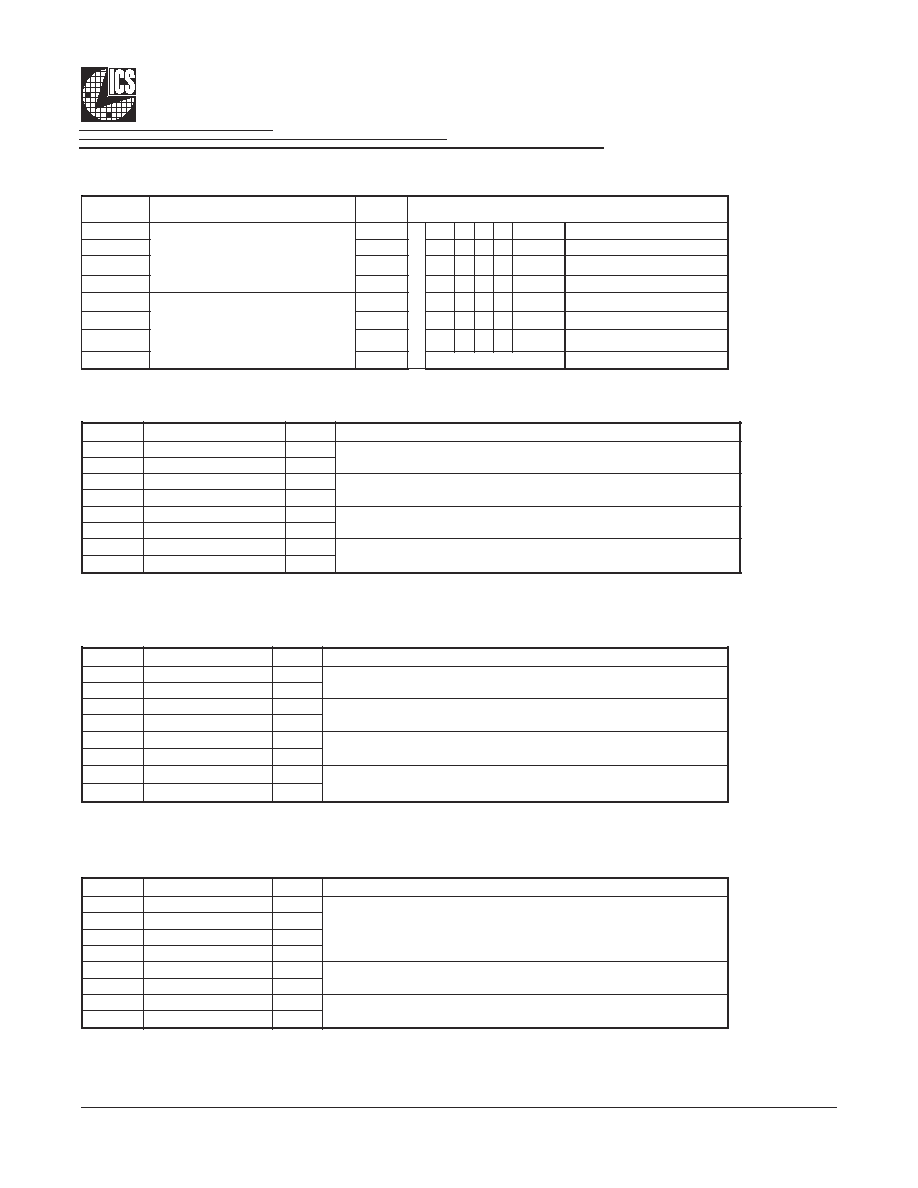
12
Integrated
Circuit
Systems, Inc.
ICS950219
Preliminary Product Preview
0640C--05/28/03
Byte 20: Group Skew Control Register
Byte 21: Slew Rate Control Register
Byte 22: Slew Rate Control Register
Byte 23: Slew Rate Control Register
t
i
B
e
m
a
N
D
W
P
n
o
i
t
p
i
r
c
s
e
D
7
t
i
B
1
w
e
l
S
_
2
_
K
L
C
I
C
P
1
.
s
t
i
b
l
o
r
t
n
o
c
e
t
a
r
w
e
l
s
k
c
o
l
c
2
K
L
C
I
C
P
k
a
e
w
=
0
1
;
l
a
m
r
o
n
=
1
1
:
g
n
o
r
t
s
=
1
0
6
t
i
B
1
w
e
l
S
_
2
_
K
L
C
I
C
P
0
5
t
i
B
0
w
e
l
S
_
)
0
:
1
(
K
L
C
I
C
P
1
.
s
t
i
b
l
o
r
t
n
o
c
e
t
a
r
w
e
l
s
k
c
o
l
c
)
0
:
1
(
K
L
C
I
C
P
k
a
e
w
=
0
1
;
l
a
m
r
o
n
=
1
1
:
g
n
o
r
t
s
=
1
0
4
t
i
B
0
w
e
l
S
_
)
0
:
1
(
K
L
C
I
C
P
0
3
t
i
B
1
w
e
l
S
_
)
2
:
3
(
6
6
V
3
1
.
s
t
i
b
l
o
r
t
n
o
c
e
t
a
r
w
e
l
s
k
c
o
l
c
)
1
:
2
(
6
6
V
3
k
a
e
w
=
0
1
;
l
a
m
r
o
n
=
1
1
:
g
n
o
r
t
s
=
1
0
2
t
i
B
1
w
e
l
S
_
)
2
:
3
(
6
6
V
3
0
1
t
i
B
1
w
e
l
S
_
)
0
:
1
(
6
6
V
3
1
.
s
t
i
b
l
o
r
t
n
o
c
e
t
a
r
w
e
l
s
k
c
o
l
c
)
0
:
1
(
6
6
V
3
k
a
e
w
=
0
1
;
l
a
m
r
o
n
=
1
1
:
g
n
o
r
t
s
=
1
0
0
t
i
B
0
w
e
l
S
_
)
0
:
1
(
6
6
V
3
0
t
i
B
e
m
a
N
D
W
P
n
o
i
t
p
i
r
c
s
e
D
7
t
i
B
1
w
e
l
S
F
E
R
1
.
s
t
i
b
l
o
r
t
n
o
c
e
t
a
r
w
e
l
s
k
c
o
l
c
F
E
R
k
a
e
w
=
0
1
;
l
a
m
r
o
n
=
1
1
:
g
n
o
r
t
s
=
1
0
6
t
i
B
0
w
e
l
S
F
E
R
0
5
t
i
B
1
w
e
l
S
)
7
:
9
(
I
C
P
1
.
s
t
i
b
l
o
r
t
n
o
c
e
t
a
r
w
e
l
s
k
c
o
l
c
)
)
7
:
9
(
I
C
P
k
a
e
w
=
0
1
;
l
a
m
r
o
n
=
1
1
:
g
n
o
r
t
s
=
1
0
4
t
i
B
0
w
e
l
S
)
7
:
9
(
I
C
P
0
3
t
i
B
)
5
:
6
(
I
C
P
1
w
e
l
S
1
.
s
t
i
b
l
o
r
t
n
o
c
e
t
a
r
w
e
l
s
k
c
o
l
c
)
5
:
6
(
I
C
P
k
a
e
w
=
0
1
;
l
a
m
r
o
n
=
1
1
:
g
n
o
r
t
s
=
1
0
2
t
i
B
)
5
:
6
(
I
C
P
0
w
e
l
S
0
1
t
i
B
)
3
:
4
(
I
C
P
1
w
e
l
S
1
.
s
t
i
b
l
o
r
t
n
o
c
e
t
a
r
w
e
l
s
k
c
o
l
c
)
3
:
4
(
I
C
P
k
a
e
w
=
0
1
;
l
a
m
r
o
n
=
1
1
:
g
n
o
r
t
s
=
1
0
0
t
i
B
)
3
:
4
(
I
C
P
0
w
e
l
S
0
t
i
B
e
m
a
N
D
W
P
n
o
i
t
p
i
r
c
s
e
D
7
t
i
B
d
e
v
r
e
s
e
R
X
d
e
v
r
e
s
e
R
6
t
i
B
d
e
v
r
e
s
e
R
X
5
t
i
B
d
e
v
r
e
s
e
R
1
4
t
i
B
d
e
v
r
e
s
e
R
0
3
t
i
B
1
w
e
l
S
z
H
M
8
4
1
.
s
t
i
b
l
o
r
t
n
o
c
e
t
a
r
w
e
l
s
k
c
o
l
c
z
H
M
8
4
k
a
e
w
=
0
1
;
l
a
m
r
o
n
=
1
1
:
g
n
o
r
t
s
=
1
0
2
t
i
B
0
w
e
l
S
z
H
M
8
4
0
1
t
i
B
1
w
e
l
S
z
H
M
8
4
_
4
2
1
.
s
t
i
b
l
o
r
t
n
o
c
e
t
a
r
w
e
l
s
k
c
o
l
c
z
H
M
8
4
_
4
2
k
a
e
w
=
0
1
;
l
a
m
r
o
n
=
1
1
:
g
n
o
r
t
s
=
1
0
0
t
i
B
0
w
e
l
S
z
H
M
8
4
_
4
2
0
t
i
B
e
m
a
N
D
W
P
e
c
n
e
u
q
e
S
g
n
i
m
m
a
r
g
o
r
P
7
t
i
B
l
o
r
t
n
o
c
s
t
i
b
4
e
s
e
h
T
)
0
:
9
(
I
C
P
-
U
P
C
1
0
0 0 0
s
p
0
d
e
v
r
e
s
e
R
6
t
i
B
0
0
1 0 0
s
p
0
5
1
d
e
v
r
e
s
e
R
5
t
i
B
0
1
0 0 0
s
p
0
0
3
d
e
v
r
e
s
e
R
4
t
i
B
0
1
1 0 0
s
p
0
5
4
d
e
v
r
e
s
e
R
3
t
i
B
d
e
v
e
r
s
e
R
1
1
1 0
1
s
p
0
0
6
d
e
v
r
e
s
e
R
2
t
i
B
0
1
1 1 0
s
p
0
5
7
d
e
v
r
e
s
e
R
1
t
i
B
0
1
1 1 1
s
p
0
0
9
d
e
v
r
e
s
e
R
0
t
i
B
0
d
e
v
r
e
s
e
R
d
e
v
r
e
s
e
R
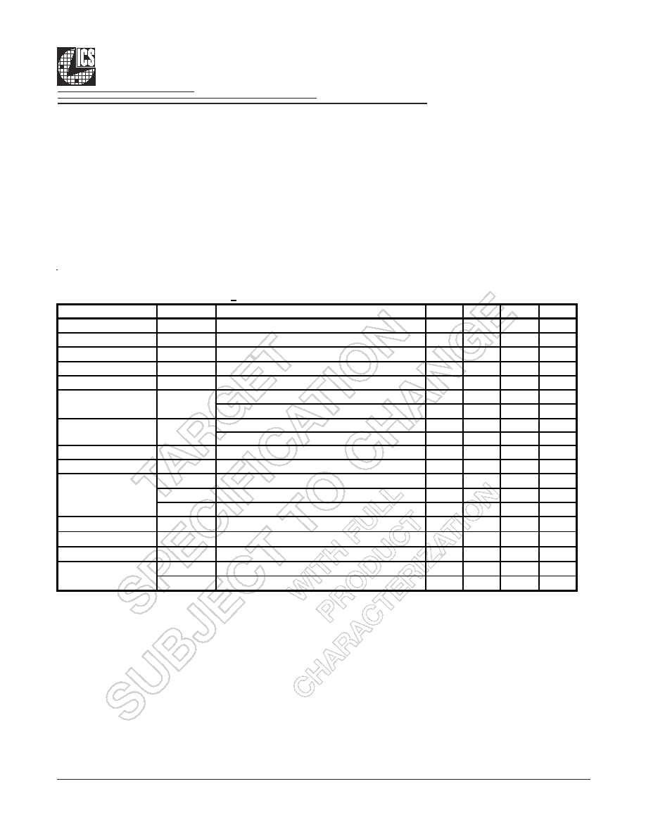
13
Integrated
Circuit
Systems, Inc.
ICS950219
Preliminary Product Preview
0640C--05/28/03
Absolute Maximum Ratings
Supply Voltage . . . . . . . . . . . . . . . . . . . . . . . . . . . . . . . . 5.5 V
Logic Inputs . . . . . . . . . . . . . . . . . . . . . . . . . . . . . . . . . . GND ≠0.5 V to V
DD
+0.5 V
Ambient Operating Temperature . . . . . . . . . . . . . . . . . 0∞C to +70∞C
Case Temperature . . . . . . . . . . . . . . . . . . . . . . . . . . . . . 115∞C
Storage Temperature . . . . . . . . . . . . . . . . . . . . . . . . . . . ≠65∞C to +150∞C
Stresses above those listed under
Absolute Maximum Ratings may cause permanent damage to the device. These ratings are
stress specifications only and functional operation of the device at these or any other conditions above those listed in the
operational sections of the specifications is not implied. Exposure to absolute maximum rating conditions for extended
periods may affect product reliability.
Electrical Characteristics - Input/Supply/Common Output Parameters
T
A
= 0 - 70C; Supply Voltage V
DD
= 3.3 V +5%
PARAMETER
SYMBOL
CONDITIONS
MIN
TYP
MAX
UNITS
Input High Voltage
V
IH
2
V
DD
+0.3
V
Input Low Voltage
V
IL
V
SS
-0.3
0.8
V
Input High Current
I
IH
V
IN
= V
DD
-5
5
mA
Input Low Current
I
IL1
V
IN
= 0 V; Inputs with no pull-up resistors
-5
mA
Input Low Current
I
IL2
V
IN
= 0 V; Inputs with pull-up resistors
-200
mA
Operating
C
L
= 0 pF; Select @ 66M
100
mA
Supply Current
C
L
= Full load
360
mA
IREF=2.32
25
mA
IREF= 5mA
45
mA
Input frequency
F
i
V
DD
= 3.3 V;
14.318
MHz
Pin Inductance
L
pin
7
nH
C
IN
Logic Inputs
5
pF
C
out
Out put pin capacitance
6
pF
C
INX
X1 & X2 pins
27
36
45
pF
Transition Time
1
T
trans
To 1st crossing of target Freq.
3
mS
Settling Time
1
T
s
From 1st crossing to 1% target Freq.
3
mS
Clk Stabilization
1
T
STAB
From V
DD
= 3.3 V to 1% target Freq.
3
mS
t
PZH
,t
PZH
output enable delay (all outputs)
1
10
nS
t
PLZ
,t
PZH
output disable delay (all outputs)
1
10
nS
1
Guarenteed by design, not 100% tested in production.
Input Capacitance
1
Delay
I
DD3.3OP
Power Down
Supply Current
I
DD3.3PD

14
Integrated
Circuit
Systems, Inc.
ICS950219
Preliminary Product Preview
0640C--05/28/03
Electrical Characteristics - CPU 0.7V Current Mode Differential Pair
T
A
= 0 - 70∞C; V
DD
= 3.3 V +/-5%; C
L
=2pF
PARAMETER
SYMBOL
CONDITIONS
MIN
TYP
MAX
UNITS
NOTES
Current Source Output
Impedance
Zo
1
V
O
= V
x
3000
1
Voltage High
VHigh
660
770
850
1
Voltage Low
VLow
-150
5
150
1
Max Voltage
Vovs
756
1150
1
Min Voltage
Vuds
-300
-7
1
Crossing Voltage (abs) Vcross(abs)
250
350
550
mV
1
Crossing Voltage (var)
d-Vcross
Variation of crossing over all
edges
12
140
mV
1
Long Accuracy
ppm
see Tperiod min-max values
-300
300
ppm
1,2
200MHz nominal
4.9985
5.0015
ns
2
200MHz spread
4.9985
5.0266
ns
2
166.66MHz nominal
5.9982
6.0018
ns
2
166.66MHz spread
5.9982
6.0320
ns
2
133.33MHz nominal
7.4978
7.5023
ns
2
133.33MHz spread
7.4978
5.4000
ns
2
100.00MHz nominal
9.9970
10.0030
ns
2
100.00MHz spread
9.9970
10.0533
ns
2
200MHz nominal
4.8735
ns
1,2
166.66MHz nominal/spread
5.8732
ns
1,2
133.33MHz nominal/spread
7.3728
ns
1,2
100.00MHz nominal/spread
9.8720
ns
1,2
Rise Time
t
r
V
OL
= 0.175V, V
OH
= 0.525V
175
332
700
ps
1
Fall Time
t
f
V
OH
= 0.525V V
OL
= 0.175V
175
344
700
ps
1
Rise Time Variation
d-t
r
30
125
ps
1
Fall Time Variation
d-t
f
30
125
ps
1
Duty Cycle
d
t3
Measurement from differential
wavefrom
45
49
55
%
1
Skew
t
sk3
V
T
= 50%
8
100
ps
1
Jitter, Cycle to cycle
t
jcyc-cyc
Measurement from differential
wavefrom
60
150
ps
1
1
Guaranteed by design, not 100% tested in production.
Statistical measurement on single
ended signal using oscilloscope
math function.
mV
Measurement on single ended
signal using absolute value.
mV
2
All Long Term Accuracy and Clock Period specifications are guaranteed with the assumption that Ref output is at
14.31818MHz
Tperiod
Average period
Absolute min period
T
absmin
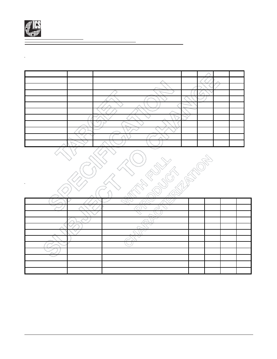
15
Integrated
Circuit
Systems, Inc.
ICS950219
Preliminary Product Preview
0640C--05/28/03
Electrical Characteristics - 3V66
T
A
= 0 - 70∞C; V
DD
= 3.3 V +/-5%; C
L
=10-30 pF (unless otherwise stated)
PARAMETER
SYMBOL
CONDITIONS
MIN
TYP
MAX
UNITS
Output Frequency
F
O1
66.66
MHz
Output Impedance
R
DSP1
1
V
O
= V
DD
*(0.5)
12
55
Output High Voltage
V
OH1
I
OH
= -1 mA
2.4
V
Output Low Voltage
V
OL1
I
OL
= 1 mA
0.4
V
Output High Current
I
OH1
V
OH
@ MIN = 1.0 V, V
OH
@ MAX = 3.135 V
-33
-33
mA
Output Low Current
I
OL1
V
OL
@ MIN = 1.95 V, V
OL
@ MAX= 0.4
30
38
mA
Rise Time
t
r1
1
V
OL
= 0.4 V, V
OH
= 2.4 V
0.5
2
ns
Fall Time
t
f1
1
V
OH
= 2.4 V, V
OL
= 0.4 V
0.5
2
ns
Duty Cycle
d
t1
1
V
T
= 1.5 V
45
55
%
Skew
t
sk1
1
V
T
= 1.5 V
250
ps
Jitter
tjcyc-cyc
1
V
T
= 1.5 V
250
ps
1
Guaranteed by design, not 100% tested in production.
Electrical Characteristics - PCICLK
T
A
= 0 - 70∞C; V
DD
= 3.3 V +/-5%; C
L
= 10-30 pF (unless otherwise stated)
PARAMETER
SYMBOL
CONDITIONS
MIN
TYP
MAX
UNITS
Output Frequency
F0
1
33.33
MHz
Output Impedance
R
DSN1
1
V
O
= V
DD
*(0.5)
12
55
Output High Voltage
V
OH1
I
OH
= -1 mA
2.4
V
Output Low Voltage
V
OL1
I
OL
= 1 mA
0.55
V
Output High Current
I
OH1
VOH@ MIN = 1.0 V, VOH@ MAX = 3.135 V
-33
-33
mA
Output Low Current
I
OL1
VOL@ MIN = 1.95 V, VOL@ MAX= 0.4
30
38
mA
Rise Time
t
r1
1
V
OL
= 0.4 V, V
OH
= 2.4 V
0.5
2
ns
Fall Time
t
f1
1
V
OH
= 2.4 V, V
OL
= 0.4 V
0.5
2
ns
Duty Cycle
d
t1
1
V
T
= 1.5 V
45
55
%
Skew
t
sk1
1
V
T
= 1.5 V
500
ps
Jitter
t
jcyc-cyc
1
V
T
= 1.5 V
250
ps
1
Guaranteed by design, not 100% tested in production.

16
Integrated
Circuit
Systems, Inc.
ICS950219
Preliminary Product Preview
0640C--05/28/03
Electrical Characteristics - REF
T
A
= 0 - 70∞C; V
DD
= 3.3 V +/-5%; C
L
=10-20 pF (unless otherwise stated)
PARAMETER
SYMBOL
CONDITIONS
MIN
TYP
MAX
UNITS
Output Frequency
F
O
14.318
MHz
Output Impedance
R
DSP1
1
V
O
= V
DD
*(0.5)
20
60
Output High Voltage
V
OH1
I
OH
= -1 mA
2.4
V
Output Low Voltage
V
OL1
I
OL
= 1 mA
0.4
V
Output High Current
I
OH1
VOH@ MIN = 1.0 V, VOH@ MAX = 3.135 V
-29
-23
mA
Output Low Current
I
OL1
VOL@ MIN = 1.95 V, VOL@ MAX= 0.4
29
27
mA
Rise Time
t
r1
1
V
OL
= 0.4 V, V
OH
= 2.4 V
1
4
ns
Fall Time
t
f1
1
V
OH
= 2.4 V, V
OL
= 0.4 V
1
4
ns
Duty Cycle
d
t1
1
V
T
= 1.5 V
45
55
%
Jitter
t
jcyc-cyc
V
T
= 1.5 V
1000
ps
1
Guaranteed by design, not 100% tested in production.
Electrical Characteristics - 48MHz
T
A
= 0 - 70∞C; V
DD
= 3.3 V +/-5%; C
L
= 10-30 pF (unless otherwise stated)
PARAMETER
SYMBOL
CONDITIONS
MIN
TYP
MAX
UNITS
Output Frequency
F
O
1
V
O
= V
DD
*(0.5)
48.008
MHz
Output Impedance
R
DSN1
1
V
O
= V
DD
*(0.5)
12
55
Output High Voltage
V
OH1
I
OH
= -1 mA
2.4
V
Output Low Voltage
V
OL1
I
OL
= 1 mA
0.55
V
Output High Current
I
OH1
V
OH
@ MIN = 1.0 V, V
OH
@ MAX = 3.135 V
-29
-23
mA
Output Low Current
I
OL1
V
OL
@ MIN = 1.95 V, V
OL
@ MAX= 0.4
29
27
mA
48DOT Rise Time
t
r1
1
V
OL
= 0.4 V, V
OH
= 2.4 V
0.5
1
ns
48DOT Fall Time
t
f1
1
V
OH
= 2.4 V, V
OL
= 0.4 V
0.5
1
ns
VCH 48 USB
Rise Time
t
r
1
V
OL
= 0.4 V, V
OH
= 2.4 V
1
2
ns
VCH 48 USB
Fall Time
tf
1
V
OH
= 2.4 V, V
OL
= 0.4 V
1
2
ns
48 DOT to 48 USB
Skew
tskew
1
VT=1.5V
1
ns
Duty Cycle
d
t1
1
V
T
= 1.5 V
45
55
%
Jitter
t
jcyc-cyc
1
V
T
= 1.5 V
350
ps
1
Guaranteed by design, not 100% tested in production.
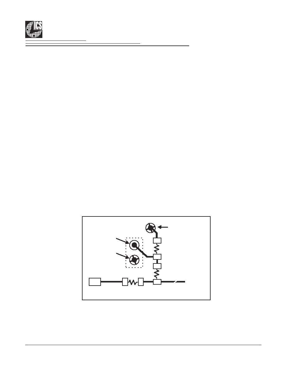
17
Integrated
Circuit
Systems, Inc.
ICS950219
Preliminary Product Preview
0640C--05/28/03
Fig. 1
Shared Pin Operation -
Input/Output Pins
The I/O pins designated by (input/output) serve as dual
signal functions to the device. During initial power-up, they
act as input pins. The logic level (voltage) that is present on
these pins at this time is read and stored into a 5-bit internal
data latch. At the end of Power-On reset, (see AC
characteristics for timing values), the device changes the
mode of operations for these pins to an output function. In
this mode the pins produce the specified buffered clocks to
external loads.
To program (load) the internal configuration register for
these pins, a resistor is connected to either the VDD (logic 1)
power supply or the GND (logic 0) voltage potential. A 10
Kilohm (10K) resistor is used to provide both the solid CMOS
programming voltage needed during the power-up
programming period and to provide an insignificant load on
the output clock during the subsequent operating period.
Via to
VDD
Clock trace to load
Series Term. Res.
Programming
Header
Via to Gnd
Device
Pad
2K
W
8.2K
W
Figure 1 shows a means of implementing this function
when a switch or 2 pin header is used. With no jumper is
installed the pin will be pulled high. With the jumper in
place the pin will be pulled low. If programmability is not
necessary, than only a single resistor is necessary. The
programming resistors should be located close to the series
termination resistor to minimize the current loop area. It is
more important to locate the series termination resistor
close to the driver than the programming resistor.

Integrated
Circuit
Systems, Inc.
ICS950219
Preliminary Product Preview
0640C--05/28/03
All 3V66 clocks are to be in pphase with each other. In the case where 3V66_1 is configured as 48MHz VCH clock, there is no
defined phase relationship between 3V66_1/VCH and other 3V66 clocks. The PCI group should lag 3V66 by the standard
skew described below as Tpci.
Un-Buffered Mode 3V66 & PCI Phase Relationship
3V66
PCICLK_F and PCICLK
Tpci
Group Skews at Common Transition Edges: (Un-Buffered Mode)
GROUP
SYMBOL
CONDITIONS
MIN
TYP
MAX
UNITS
3V66
3V66
3V66 pin to pin skew
0
500
ps
PCI
PCI
PCI_F and PCI pin to pin skew
0
500
ps
3V66 to PCI
S
3V66-PCI
3V66 leads 33MHz PCI
1.5
3.5
ns
1
Guarenteed by design, not 100% tested in production.

Integrated
Circuit
Systems, Inc.
ICS950219
Preliminary Product Preview
0640C--05/28/03
For more information on Integrated Circuit Systems Inc. or any of our products please visit our web site at:
http://www.icst.com
Registered Company
9001
Ordering Information
ICS950219yFT
Designation for tape and reel packaging
Package Type
F=SSOP
Revision Designator (will not correlate with datasheet revision)
Device Type
Prefix
ICS = Standard Device
Example:
ICS XXXX y F - T
INDEX
AREA
INDEX
AREA
1 2
1 2
N
D
h x 45∞
h x 45∞
E1
E
a
SEATING
PLANE
SEATING
PLANE
A1
A
e
- C -
- C -
b
.10 (.004) C
.10 (.004) C
c
L
300 mil SSOP Package
MIN
MAX
MIN
MAX
A
2.41
2.80
.095
.110
A1
0.20
0.40
.008
.016
b
0.20
0.34
.008
.0135
c
0.13
0.25
.005
.010
D
E
10.03
10.68
.395
.420
E1
7.40
7.60
.291
.299
e
h
0.38
0.64
.015
.025
L
0.50
1.02
.020
.040
N
0∞
8∞
0∞
8∞
MIN
MAX
MIN
MAX
48
15.75
16.00
.620
.630
10-0034
SYMBOL
In Millimeters
In Inches
COMMON DIMENSIONS
COMMON DIMENSIONS
SEE VARIATIONS
SEE VARIATIONS
0.635 BASIC
0.025 BASIC
Reference Doc.: JEDEC Publication 95, MO-118
VARIATIONS
SEE VARIATIONS
SEE VARIATIONS
N
D mm.
D (inch)