 | –≠–ª–µ–∫—Ç—Ä–æ–Ω–Ω—ã–π –∫–æ–º–ø–æ–Ω–µ–Ω—Ç: ICS950602 | –°–∫–∞—á–∞—Ç—å:  PDF PDF  ZIP ZIP |
Integrated
Circuit
Systems, Inc.
ICS950602
0469B--12/18/02
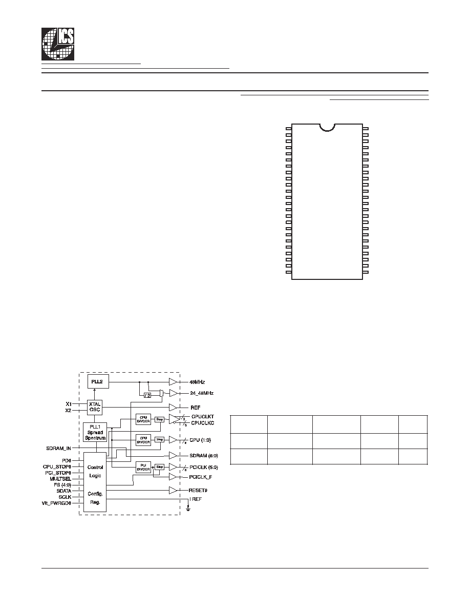
Block Diagram
Pin Configuration
Recommended Application:
VIA Mobile PL133T and PLE133T Chipsets.
Output Features:
∑
2 - CPU clocks @ 2.5V
∑
1 - Pairs of differential CPU clocks @ 3.3V
∑
7 - PCI including 1 free running @ 3.3V
∑
7 - SDRAM @ 3.3V
∑
1 - 48MHz @ 3.3V fixed
∑
1 - 24_48MHz selectable @ 3.3V
∑
2 - REF @ 3.3V, 14.318MHz
Features/Benefits:
∑
Programmable output frequency.
∑
Programmable output divider ratios.
∑
Programmable output rise/fall time.
∑
Programmable output skew.
∑
Programmable spread percentage for EMI control.
∑
Watchdog timer technology to reset system
if system malfunctions.
∑
Programmable watch dog safe frequency.
∑
Support I
2
C Index read/write and block read/write
operations.
∑
Uses external 14.318MHz crystal.
Key Specifications:
∑
CPU Output Jitter <200ps
∑
CPU Output Skew <175ps
∑
PCI to PCI Output Skew <500ps
Programmable Timing Control HubTM for P
II
/
III
TM
* Internal Pull-up resistor of 120K to VDD
** these inputs have 120K internal pull-down
to GND
48-Pin SSOP & TSSOP
GND
*FS2/REF1
REF0
Vtt_PWRGD#
VDDREF
GND
X1
X2
VDDPCI
*FS4/PCICLK_F
*FS3/PCICLK0
GND
PCICLK1
PCICLK2
PCICLK3
PCICLK4
PCICLK5
SDRAM_IN
*CPU_STOP#
*PCI_STOP#
*PD#
**MULTISEL
GND
SDATA
CPUCLK0
CPUCLK1
VDDCPU_2.5
VDDCPU_3.3
CPUCLKT
CPUCLKC
GND
RESET#
I REF
SDRAM6
GND
SDRAM0
SDRAM1
VDDSDRAM
SDRAM2
SDRAM3
GND
SDRAM4
SDRAM5
VDDSDRAM
AVDD48
48MHz/FS0*
24_48MHz/FS1*
SCLK
ICS950602
1
2
3
4
5
6
7
8
9
10
11
12
13
14
15
16
17
18
19
20
21
22
23
24
48
47
46
45
44
43
42
41
40
39
38
37
36
35
34
33
32
31
30
29
28
27
26
25
Host Swing Select Functions
0
L
E
S
I
T
L
U
M
t
e
g
r
a
T
d
r
a
o
B
Z
m
r
e
T
/
e
c
a
r
T
,
R
e
c
n
e
r
e
f
e
R
V
=
f
e
r
I
D
D
)
r
R
*
3
(
/
t
u
p
t
u
O
t
n
e
r
r
u
C
Z
@
h
o
V
0
s
m
h
o
0
5
,
%
1
1
2
2
=
r
R
A
m
0
0
.
5
=
f
e
r
I
F
E
R
I
*
4
=
h
o
I
0
5
@
V
0
.
1
1
s
m
h
o
0
5
,
%
1
5
7
4
=
r
R
A
m
2
3
.
2
=
f
e
r
I
F
E
R
I
*
6
=
h
o
I
0
5
@
V
7
.
0

2
Integrated
Circuit
Systems, Inc.
ICS950602
0469B--12/18/02
Pin Description
The ICS950602 is a single chip clock solution for VIA Mobile PL133T and PLE133T chipsets. It provides all necessary clock
signals for such a system.
The ICS950602 is part of a whole new line of ICS clock generators and buffers called TCHTM (Timing Control Hub). ICS is the
first to introduce a whole product line which offers full programmability and flexibility on a single clock device. This part
incorporates ICS's newest clock technology which offers more robust features and functionality. Employing the use of a
serially programmable I
2
C interface, this device can adjust the output clocks by configuring the frequency setting, the output
divider ratios, selecting the ideal spread percentage, the output skew, the output strength, and enabling/disabling each
individual output clock. TCH also incorporates ICS's Watchdog Timer technology and a reset feature to provide a safe setting
under unstable system conditions. M/N control can configure output frequency with resolution up to 0.1MHz increment. With
all these programmable features, ICS' TCH makes motherboard testing, tuning and improvement very simple.
General Description
R
E
B
M
U
N
N
I
P
E
M
A
N
N
I
P
E
P
Y
T
N
O
I
T
P
I
R
C
S
E
D
,
3
2
,
2
1
,
6
,
1
,
2
4
,
8
3
,
2
3
D
N
G
R
W
P
y
l
p
p
u
s
V
3
.
3
r
o
f
s
n
i
p
d
n
u
o
r
G
5
3
,
9
2
,
9
,
5
D
D
V
R
W
P
y
l
p
p
u
s
r
e
w
o
p
V
3
.
3
2
2
S
F
N
I
.
n
o
r
e
w
o
p
t
a
d
e
h
c
t
a
l
t
u
p
n
I
.
t
i
b
t
c
e
l
e
s
y
c
n
e
u
q
e
r
f
t
u
p
n
i
c
i
g
o
L
1
F
E
R
T
U
O
.
t
u
p
t
u
o
k
c
o
l
c
e
c
n
e
r
e
f
e
r
z
H
M
8
1
3
.
4
1
,
V
3
.
3
3
0
F
E
R
T
U
O
.
t
u
p
t
u
o
k
c
o
l
c
e
c
n
e
r
e
f
e
r
z
H
M
8
1
3
.
4
1
,
V
3
.
3
4
#
D
G
R
W
P
_
t
t
V
N
I
)
0
:
4
(
S
F
n
e
h
w
e
n
i
m
r
e
t
e
d
o
t
d
e
s
u
e
b
o
r
t
s
e
v
i
t
i
s
n
e
s
l
e
v
e
l
a
s
i
t
u
p
n
i
L
T
T
V
L
V
3
.
3
s
i
h
T
)
w
o
l
e
v
i
t
c
a
(
d
e
l
p
m
a
s
e
b
o
t
y
d
a
e
r
e
r
a
d
n
a
d
il
a
v
e
r
a
7
1
X
N
I
2
X
m
o
r
f
r
o
t
s
i
s
e
r
k
c
a
b
d
e
e
f
d
n
a
)
F
p
3
3
(
p
a
c
d
a
o
l
l
a
n
r
e
t
n
i
s
a
h
,
t
u
p
n
i
l
a
t
s
y
r
C
8
2
X
T
U
O
)
F
p
3
3
(
p
a
c
d
a
o
l
l
a
n
r
e
t
n
i
s
a
H
.
z
H
M
8
1
3
.
4
1
y
l
l
a
n
i
m
o
n
,
t
u
p
t
u
o
l
a
t
s
y
r
C
0
1
4
S
F
N
I
.
n
o
r
e
w
o
p
t
a
d
e
h
c
t
a
l
t
u
p
n
I
.
t
i
b
t
c
e
l
e
s
y
c
n
e
u
q
e
r
f
t
u
p
n
i
c
i
g
o
L
F
_
K
L
C
I
C
P
T
U
O
t
u
p
t
u
o
k
c
o
l
c
I
C
P
V
3
.
3
1
1
3
S
F
N
I
.
n
o
r
e
w
o
p
t
a
d
e
h
c
t
a
l
t
u
p
n
I
.
t
i
b
t
c
e
l
e
s
y
c
n
e
u
q
e
r
f
t
u
p
n
i
c
i
g
o
L
0
K
L
C
I
C
P
T
U
O
t
u
p
t
u
o
k
c
o
l
c
I
C
P
V
3
.
3
3
1
,
4
1
,
5
1
,
6
1
,
7
1
)
1
:
5
(
K
L
C
I
C
P
T
U
O
s
t
u
p
t
u
o
k
c
o
l
c
I
C
P
V
3
.
3
8
1
N
I
_
M
A
R
D
S
N
I
.
n
i
p
t
u
p
n
i
r
e
f
f
u
b
M
A
R
D
S
9
1
#
P
O
T
S
_
U
P
C
N
I
w
o
l
t
u
p
n
i
n
e
h
w
,
l
e
v
e
l
0
c
i
g
o
l
t
a
s
k
c
o
l
c
s
K
L
C
U
P
C
l
l
a
s
p
o
t
S
0
2
#
P
O
T
S
_
I
C
P
N
I
,
l
e
v
e
l
0
c
i
g
o
l
t
a
s
k
c
o
l
c
F
_
K
L
C
I
C
P
e
h
t
s
e
d
i
s
e
b
s
K
L
C
I
C
P
l
l
a
s
p
o
t
S
w
o
l
t
u
p
n
i
n
e
h
w
1
2
#
D
P
N
I
w
o
l
a
o
t
n
i
e
c
i
v
e
d
e
h
t
n
w
o
d
r
e
w
o
p
o
t
d
e
s
u
n
i
p
t
u
p
n
i
w
o
l
e
v
i
t
c
a
s
u
o
n
o
r
h
c
n
y
s
A
e
r
a
l
a
t
s
y
r
c
e
h
t
d
n
a
O
C
V
e
h
t
d
n
a
d
e
l
b
a
s
i
d
e
r
a
s
k
c
o
l
c
l
a
n
r
e
t
n
i
e
h
T
.
e
t
a
t
s
r
e
w
o
p
.
s
m
3
n
a
h
t
r
e
t
a
e
r
g
e
b
t
o
n
l
l
i
w
n
w
o
d
r
e
w
o
p
e
h
t
f
o
y
c
n
e
t
a
l
e
h
T
.
d
e
p
p
o
t
s
2
2
L
E
S
T
L
U
M
N
I
.
s
t
u
p
t
u
o
U
P
C
r
o
f
r
e
i
l
p
i
t
l
u
m
t
n
e
r
r
u
c
e
h
t
g
n
i
t
c
e
l
e
s
r
o
f
t
u
p
n
i
L
T
T
V
L
V
3
.
3
4
2
A
T
A
D
S
O
/
I
I
r
o
f
n
i
p
a
t
a
D
2
t
n
a
r
e
l
o
t
V
5
y
r
t
i
u
c
r
i
c
C
5
2
K
L
C
S
N
I
I
r
o
f
n
i
p
k
c
o
l
C
2
t
n
a
r
e
l
o
t
V
5
y
r
t
i
u
c
r
i
c
C
6
2
1
S
F
N
I
.
n
o
r
e
w
o
p
t
a
d
e
h
c
t
a
l
t
u
p
n
I
.
t
i
b
t
c
e
l
e
s
y
c
n
e
u
q
e
r
f
t
u
p
n
i
c
i
g
o
L
z
H
M
4
2
_
8
4
T
U
O
t
u
p
t
u
o
z
H
M
4
2
r
o
8
4
e
l
b
a
t
c
e
l
e
S
7
2
0
S
F
N
I
.
n
o
r
e
w
o
p
t
a
d
e
h
c
t
a
l
t
u
p
n
I
.
t
i
b
t
c
e
l
e
s
y
c
n
e
u
q
e
r
f
t
u
p
n
i
c
i
g
o
L
z
H
M
8
4
T
U
O
.
t
u
p
t
u
o
k
c
o
l
c
z
H
M
8
4
d
e
x
i
F
V
3
.
3
8
2
8
4
D
D
V
A
R
W
P
.
s
t
u
p
t
u
o
z
H
M
4
2
r
o
8
4
r
o
f
y
l
p
p
u
s
r
e
w
o
p
g
o
l
a
n
a
V
3
.
3
,
6
3
,
4
3
,
3
3
,
1
3
,
0
3
9
3
,
7
3
)
6
,
0
:
5
(
M
A
R
D
S
T
U
O
.
s
t
u
p
t
u
o
k
c
o
l
c
M
A
R
D
S
0
4
F
E
R
I
T
U
O
s
e
r
i
u
q
e
r
n
i
p
s
i
h
T
.
s
r
i
a
p
K
L
C
U
P
C
e
h
t
r
o
f
t
n
e
r
r
u
c
e
c
n
e
r
e
f
e
r
e
h
t
s
e
h
s
il
b
a
t
s
e
n
i
p
s
i
h
T
e
t
a
i
r
p
o
r
p
p
a
e
h
t
h
s
il
b
a
t
s
e
o
t
r
e
d
r
o
n
i
d
n
u
o
r
g
o
t
d
e
i
t
r
o
t
s
i
s
e
r
n
o
i
s
i
c
e
r
p
d
e
x
i
f
a
.
t
n
e
r
r
u
c
1
4
#
T
E
S
E
R
T
U
O
s
i
h
T
.
t
u
o
e
m
i
t
r
e
m
i
t
g
o
d
h
c
t
a
w
r
o
e
u
l
a
v
y
c
n
e
u
q
e
r
f
r
o
f
l
a
n
g
i
s
t
e
s
e
r
m
e
t
s
y
s
e
m
i
t
l
a
e
R
.
w
o
l
e
v
i
t
c
a
s
i
l
a
n
g
i
s
3
4
C
K
L
C
U
P
C
T
U
O
s
t
u
p
t
u
o
t
n
e
r
r
u
c
e
r
a
e
s
e
h
T
.
s
t
u
p
t
u
o
U
P
C
r
i
a
p
l
a
i
t
n
e
r
e
f
f
i
d
f
o
k
c
o
l
c
"
y
r
a
t
n
e
m
e
l
p
m
o
C
"
.
s
a
i
b
e
g
a
t
l
o
v
r
o
f
d
e
r
i
u
q
e
r
e
r
a
s
r
o
t
s
i
s
e
r
l
a
n
r
e
t
x
e
d
n
a
4
4
T
K
L
C
U
P
C
T
U
O
d
n
a
s
t
u
p
t
u
o
t
n
e
r
r
u
c
e
r
a
e
s
e
h
T
.
s
t
u
p
t
u
o
U
P
C
r
i
a
p
l
a
i
t
n
e
r
e
f
f
i
d
f
o
k
c
o
l
c
"
e
u
r
T
"
.
s
a
i
b
e
g
a
t
l
o
v
r
o
f
d
e
r
i
u
q
e
r
e
r
a
s
r
o
t
s
i
s
e
r
l
a
n
r
e
t
x
e
5
4
3
.
3
_
U
P
C
D
D
V
R
W
P
.
s
k
c
o
l
c
l
a
i
t
n
e
r
e
f
f
i
d
U
P
C
r
o
f
r
e
w
o
p
V
3
.
3
6
4
5
.
2
_
U
P
C
D
D
V
R
W
P
.
s
k
c
o
l
c
U
P
C
r
o
f
r
e
w
o
p
V
5
.
2
8
4
,
7
4
)
0
:
1
(
K
L
C
U
P
C
T
U
O
.
s
t
u
p
t
u
o
k
c
o
l
c
U
P
C

3
Integrated
Circuit
Systems, Inc.
ICS950602
0469B--12/18/02
General I
2
C serial interface information
How to Write:
∑
Controller (host) sends a start bit.
∑ Controller (host) sends the write address D2
(H)
∑ ICS clock will
acknowledge
∑ Controller (host) sends the begining byte location = N
∑ ICS clock will
acknowledge
∑ Controller (host) sends the data byte count = X
∑ ICS clock will
acknowledge
∑ Controller (host) starts sending
Byte N through
Byte N + X -1
(see Note 2)
∑ ICS clock will
acknowledge each byte one at a time
∑ Controller (host) sends a Stop bit
How to Read:
∑ Controller (host) will send start bit.
∑ Controller (host) sends the write address D2
(H)
∑ ICS clock will
acknowledge
∑ Controller (host) sends the begining byte
location = N
∑ ICS clock will
acknowledge
∑ Controller (host) will send a separate start bit.
∑ Controller (host) sends the read address D3
(H)
∑ ICS clock will
acknowledge
∑ ICS clock will send the data byte count = X
∑ ICS clock sends
Byte N + X -1
∑ ICS clock sends
Byte 0 through byte X (if X
(H)
was written to byte 8)
.
∑ Controller (host) will need to acknowledge each byte
∑ Controllor (host) will send a not acknowledge bit
∑ Controller (host) will send a stop bit
*See notes on the following page
.
ICS (Slave/Receiver)
T
WR
ACK
ACK
ACK
ACK
ACK
P
stoP bit
X Byt
e
Index Block Write Operation
Slave Address D2
(H)
Beginning Byte = N
WRite
starT bit
Controller (Host)
Byte N + X - 1
Data Byte Count = X
Beginning Byte N
T
starT bit
WR
WRite
RT
Repeat starT
RD
ReaD
Beginning Byte N
Byte N + X - 1
N
Not acknowledge
P
stoP bit
Slave Address D3
(H)
Index Block Read Operation
Slave Address D2
(H)
Beginning Byte = N
ACK
ACK
Data Byte Count = X
ACK
ICS (Slave/Receiver)
Controller (Host)
X Byt
e
ACK
ACK

4
Integrated
Circuit
Systems, Inc.
ICS950602
0469B--12/18/02
Byte 0: Functionality and frequency select register (Default=0)
Notes:
1. Default at power-up will be for latched logic inputs to define frequency, as displayed by Bit 3.
t
i
B
n
o
i
t
p
i
r
c
s
e
D
D
W
P
t
i
B
)
4
:
6
,
1
:
2
(
2
t
i
B
1
t
i
B
6
t
i
B
5
t
i
B
4
t
i
B
K
L
C
U
P
C
z
H
M
K
L
C
I
C
P
z
H
M
%
d
a
e
r
p
S
1
e
t
o
N
4
S
F
3
S
F
2
S
F
1
S
F
0
S
F
0
0
0
0
0
0
0
.
0
0
2
0
3
.
3
3
d
a
e
r
p
s
r
e
t
n
e
c
%
5
2
.
0
-
/
+
0
0
0
0
1
0
0
.
0
9
1
0
0
.
8
3
d
a
e
r
p
s
r
e
t
n
e
c
%
5
2
.
0
-
/
+
0
0
0
1
0
0
0
.
0
8
1
0
0
.
6
3
d
a
e
r
p
s
r
e
t
n
e
c
%
5
2
.
0
-
/
+
0
0
0
1
1
0
0
.
0
7
1
0
0
.
4
3
d
a
e
r
p
s
r
e
t
n
e
c
%
5
2
.
0
-
/
+
0
0
1
0
0
0
0
.
6
6
1
0
2
.
3
3
d
a
e
r
p
s
r
e
t
n
e
c
%
5
2
.
0
-
/
+
0
0
1
0
1
0
0
.
0
6
1
0
0
.
2
3
d
a
e
r
p
s
r
e
t
n
e
c
%
5
2
.
0
-
/
+
0
0
1
1
0
0
0
.
0
5
1
0
5
.
7
3
d
a
e
r
p
s
r
e
t
n
e
c
%
5
2
.
0
-
/
+
0
0
1
1
1
0
0
.
5
4
1
0
3
.
6
3
d
a
e
r
p
s
r
e
t
n
e
c
%
5
2
.
0
-
/
+
0
1
0
0
0
0
0
.
0
4
1
0
0
.
5
3
d
a
e
r
p
s
r
e
t
n
e
c
%
5
2
.
0
-
/
+
0
1
0
0
1
0
0
.
6
3
1
0
0
.
4
3
d
a
e
r
p
s
r
e
t
n
e
c
%
5
2
.
0
-
/
+
0
1
0
1
0
0
0
.
0
3
1
0
5
.
2
3
d
a
e
r
p
s
r
e
t
n
e
c
%
5
2
.
0
-
/
+
0
1
0
1
1
0
0
.
4
2
1
0
0
.
1
3
d
a
e
r
p
s
r
e
t
n
e
c
%
5
2
.
0
-
/
+
0
1
1
0
0
0
2
.
7
6
0
6
.
3
3
d
a
e
r
p
s
r
e
t
n
e
c
%
5
2
.
0
-
/
+
0
1
1
0
1
0
9
.
0
0
1
3
6
.
3
3
d
a
e
r
p
s
r
e
t
n
e
c
%
5
2
.
0
-
/
+
0
1
1
1
0
0
0
.
8
1
1
0
3
.
9
3
d
a
e
r
p
s
r
e
t
n
e
c
%
5
2
.
0
-
/
+
0
1
1
1
1
0
4
.
4
3
1
0
6
.
3
3
d
a
e
r
p
s
r
e
t
n
e
c
%
5
2
.
0
-
/
+
1
0
0
0
0
0
0
.
7
6
0
5
.
3
3
d
a
e
r
p
s
r
e
t
n
e
c
%
5
2
.
0
-
/
+
1
0
0
0
1
0
5
.
0
0
1
0
5
.
3
3
d
a
e
r
p
s
r
e
t
n
e
c
%
5
2
.
0
-
/
+
1
0
0
1
0
0
0
.
5
1
1
0
3
.
8
3
d
a
e
r
p
s
r
e
t
n
e
c
%
5
2
.
0
-
/
+
1
0
0
1
1
0
9
.
3
3
1
7
4
.
3
3
d
a
e
r
p
s
r
e
t
n
e
c
%
5
2
.
0
-
/
+
1
0
1
0
0
0
8
.
6
6
0
4
.
3
3
d
a
e
r
p
s
r
e
t
n
e
c
%
5
2
.
0
-
/
+
1
0
1
0
1
0
2
.
0
0
1
0
4
.
3
3
d
a
e
r
p
s
r
e
t
n
e
c
%
5
2
.
0
-
/
+
1
0
1
1
0
0
0
.
0
1
1
0
7
.
6
3
d
a
e
r
p
s
r
e
t
n
e
c
%
5
2
.
0
-
/
+
1
0
1
1
1
0
6
.
3
3
1
0
4
.
3
3
d
a
e
r
p
s
r
e
t
n
e
c
%
5
2
.
0
-
/
+
1
1
0
0
0
0
0
.
5
0
1
0
0
.
5
3
d
a
e
r
p
s
r
e
t
n
e
c
%
5
2
.
0
-
/
+
1
1
0
0
1
0
0
.
0
9
0
0
.
0
3
d
a
e
r
p
s
r
e
t
n
e
c
%
5
2
.
0
-
/
+
1
1
0
1
0
0
0
.
5
8
0
3
.
8
2
d
a
e
r
p
s
r
e
t
n
e
c
%
5
2
.
0
-
/
+
1
1
0
1
1
0
0
.
8
7
0
0
.
9
3
d
a
e
r
p
s
r
e
t
n
e
c
%
5
2
.
0
-
/
+
1
1
1
0
0
0
6
.
6
6
0
3
.
3
3
d
a
e
r
p
s
r
e
t
n
e
c
%
5
2
.
0
-
/
+
1
1
1
0
1
0
0
.
0
0
1
0
3
.
3
3
d
a
e
r
p
s
n
w
o
d
%
5
.
0
-
o
t
0
1
1
1
1
0
0
0
.
5
7
0
5
.
7
3
d
a
e
r
p
s
r
e
t
n
e
c
%
5
2
.
0
-
/
+
1
1
1
1
1
0
3
.
3
3
1
0
3
.
3
3
d
a
e
r
p
s
n
w
o
d
%
5
.
0
-
o
t
0
3
t
i
B
s
t
u
p
n
i
d
e
h
c
t
a
l
,
t
c
e
l
e
s
e
r
a
w
d
r
a
h
y
b
d
e
t
c
e
l
e
s
s
i
y
c
n
e
u
q
e
r
F
-
0
4
:
7
,
2
t
i
B
y
b
d
e
t
c
e
l
e
s
s
i
y
c
n
e
u
q
e
r
F
-
1
0
0
t
i
B
l
a
m
r
o
N
-
0
e
l
b
a
n
e
m
u
r
t
c
e
p
s
d
a
e
r
p
S
-
1
0
7
t
i
B
s
t
u
p
n
i
h
c
t
a
l
y
b
d
e
t
c
e
l
e
s
e
b
ll
i
w
y
c
n
e
u
q
e
r
f
e
f
a
s
g
o
d
h
c
t
a
W
-
0
)
0
:
4
(
t
i
b
0
1
e
t
y
B
y
b
d
e
m
m
a
r
g
o
r
p
e
b
ll
i
w
y
c
n
e
u
q
e
r
f
e
f
a
s
g
o
d
h
c
t
a
W
-
1
0

5
Integrated
Circuit
Systems, Inc.
ICS950602
0469B--12/18/02
Byte 1: Output Control Register
(1 = enable, 0 = disable)
Byte 3: Output Control Register
(1 = enable, 0 = disable)
Byte 2: Output Control Register
(1 = enable, 0 = disable)
Byte 4: Output Control Register
(1 = enable, 0 = disable)
t
i
B
#
n
i
P
D
W
P
n
o
i
t
p
i
r
c
s
e
D
7
t
i
B
-
X
k
c
a
b
d
a
e
R
4
S
F
6
t
i
B
-
X
k
c
a
b
d
a
e
R
3
S
F
5
t
i
B
-
X
k
c
a
b
d
a
e
R
2
S
F
4
t
i
B
-
X
k
c
a
b
d
a
e
R
1
S
F
3
t
i
B
-
X
k
c
a
b
d
a
e
R
0
S
F
2
t
i
B
8
4
1
0
K
L
C
U
P
C
1
t
i
B
7
4
1
1
K
L
C
U
P
C
0
t
i
B
3
4
,
4
4
1
C
K
L
C
U
P
C
,
T
K
L
C
U
P
C
t
i
B
#
n
i
P
D
W
P
n
o
i
t
p
i
r
c
s
e
D
7
t
i
B
9
3
1
6
M
A
R
D
S
6
t
i
B
0
1
1
F
_
K
L
C
I
C
P
5
t
i
B
7
1
1
5
K
L
C
I
C
P
4
t
i
B
6
1
1
4
K
L
C
I
C
P
3
t
i
B
5
1
1
3
K
L
C
I
C
P
2
t
i
B
4
1
1
2
K
L
C
I
C
P
1
t
i
B
3
1
1
1
K
L
C
I
C
P
0
t
i
B
1
1
1
0
K
L
C
I
C
P
t
i
B
#
n
i
P
D
W
P
n
o
i
t
p
i
r
c
s
e
D
7
t
i
B
-
0
e
l
b
a
s
i
D
=
0
,
e
l
b
a
n
E
=
1
t
c
e
t
e
d
t
f
i
h
s
r
a
e
g
T
E
S
E
R
6
t
i
B
-
0
8
4
=
1
,
4
2
=
0
:
8
4
_
4
2
L
E
S
5
t
i
B
7
2
1
z
H
M
8
4
4
t
i
B
6
2
1
z
H
M
8
4
_
4
2
3
t
i
B
-
0
d
e
v
r
e
s
e
R
2
t
i
B
0
3
,
1
3
1
)
5
:
4
(
M
A
R
D
S
1
t
i
B
3
3
,
4
3
1
)
3
:
2
(
M
A
R
D
S
0
t
i
B
6
3
,
7
3
1
)
1
:
0
(
M
A
R
D
S
t
i
B
#
n
i
P
D
W
P
n
o
i
t
p
i
r
c
s
e
D
7
t
i
B
-
X
k
c
a
b
d
a
e
R
L
E
S
T
L
U
M
6
t
i
B
-
X
d
e
v
r
e
s
e
R
5
t
i
B
-
X
d
e
v
r
e
s
e
R
4
t
i
B
-
X
d
e
v
r
e
s
e
R
3
t
i
B
-
X
d
e
v
r
e
s
e
R
2
t
i
B
-
X
d
e
v
r
e
s
e
R
1
t
i
B
-
X
d
e
v
r
e
s
e
R
0
t
i
B
-
X
d
e
v
r
e
s
e
R