Integrated
Circuit
Systems, Inc.
ICS950805
0649G--06/11/02
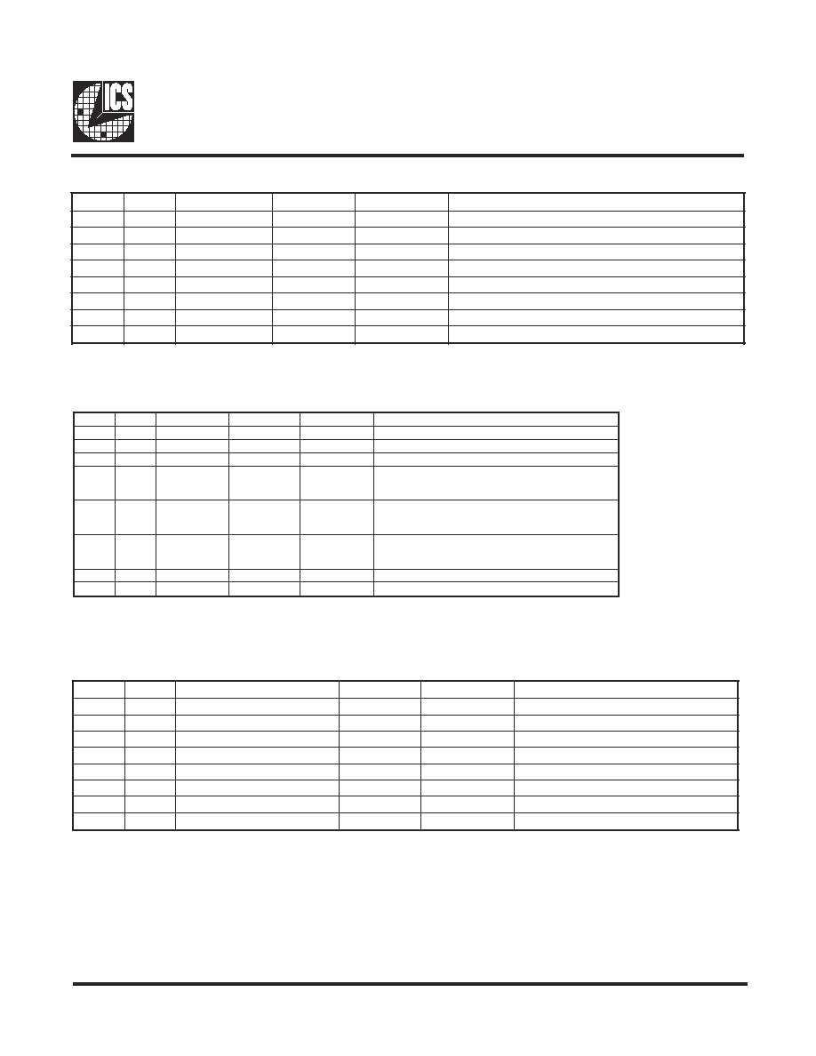
Block Diagram
Recommended Application:
CK-408 clock for Almador-M and Brookdale-Mobile
chipsets. Programmable for group to group skew.
Output Features:
∑
3 Differential CPU Clock Pairs (differential current
mode)
∑
7 PCI (3.3V) @ 33.3MHz
∑
3 PCI_F (3.3V) @ 33.3MHz
∑
1 USB (3.3V) @ 48MHz
∑
1 DOT (3.3V) @ 48MHz
∑
1 REF (3.3V) @ 14.318MHz
∑
1 3V66 (3.3V) @ 66.6MHz
∑
1 VCH/3V66 (3.3V) @ 48MHz or 66.6MHz
∑
3 66MHz_OUT/3V66 (3.3V) @ 66.6MHz_IN
or 66.6MHz
∑
1 66MHz_IN/3V66 (3.3V) @ Input/66MHz
Features:
∑
Almador Chipset has a DLL driving the clock buffer
path for the 3 buffer path 66.6 MHz outputs,
66Buf(0:2). Almador board level designs MUST
use pin 22, 66Buf_1, as the feedback connection
from the clock buffer path to the Almador
(GMCH) chipset.
∑
Supports spread spectrum modulation,
down spread 0 to -0.5%.
∑
Efficient power management scheme through PD#,
CPU_STOP# and PCI_STOP#.
Key Specifications:
∑
CPU Output Jitter <150ps
∑
3V66 Output Jitter <250ps
∑
66MHz Output Jitter (Buffered Mode Only) <100ps
∑
CPU Output Skew <100ps
Pin Configuration
56-Pin 300mil SSOP
6.10 mm. Body, 0.50 mm. pitch TSSOP
Frequency Generator with 200MHz Differential CPU Clocks
VDDREF
X1
X2
GND
PCICLK_F0
PCICLK_F1
PCICLK_F2
VDDPCI
GND
PCICLK0
PCICLK1
PCICLK2
PCICLK3
VDDPCI
GND
PCICLK4
PCICLK5
PCICLK6
VDD3V66
GND
66MHz_OUT0/3V66_2
66MHz_OUT1/3V66_3
66MHz_OUT2/3V66_4
66MHz_IN/3V66_5
*PD#
VDDA
GND
Vtt_PWRGD#
REF
FS1
FS0
CPU_STOP#*
CPUCLKT0
CPUCLKC0
VDDCPU
CPUCLKT1
CPUCLKC1
GND
VDDCPU
CPUCLKT2
CPUCLKC2
MULTSEL0*
I REF
GND
FS2
48MHz_USB
48MHz_DOT
VDD48
GND
3V66_1/VCH_CLK
PCI_STOP#*
3V66_0
VDD3V66
GND
SCLK
SDATA
ICS950805
1
2
3
4
5
6
7
8
9
10
11
12
13
14
15
16
17
18
19
20
21
22
23
24
25
26
27
28
56
55
54
53
52
51
50
49
48
47
46
45
44
43
42
41
40
39
38
37
36
35
34
33
32
31
30
29
Functionality
PLL2
PLL1
Spread
Spectrum
3V66_5/66MHz_IN
3V66_3/66MHz_OUT1
3V66_(4,2)/66MHz_OUT(2,0)
48MHz_USB
48MHz_DOT
X1
X2
XTAL
OSC
3V66
DIVDER
PD#
CPU_STOP#
PCI_STOP#
MULTSEL0
SDATA
SCLK
FS (2:0)
I REF
Control
Logic
Config.
Reg.
REF
66MHz_0
CPU
DIVDER
3
3
CPUCLKT (2:0)
CPUCLKC (2:0)
Stop
3V66_1/VCH_CLK
PCICLK (6:0)
PCI
DIVDER
3
7
PCICLK_F (2:0)
Stop
* These inputs have 150K internal pull-up resistor to VDD.
2
S
F
1
S
F
0
S
F
U
P
C
)
z
H
M
(
)
0
:
1
(
6
6
V
3
)
z
H
M
(
)
0
:
2
(
t
u
O
z
H
M
6
6
)
2
:
4
(
6
6
V
3
)
z
H
M
(
F
_
I
C
P
I
C
P
)
z
H
M
(
n
I
z
H
M
6
6
)
5
(
6
6
V
3
)
z
H
M
(
0
0
0
6
6
.
6
6
6
6
.
6
6
6
6
.
6
6
3
3
.
3
3
6
6
.
6
6
0
0
1
0
0
.
0
0
1
6
6
.
6
6
6
6
.
6
6
3
3
.
3
3
6
6
.
6
6
0
1
0
0
0
.
0
0
2
6
6
.
6
6
6
6
.
6
6
3
3
.
3
3
6
6
.
6
6
0
1
1
3
3
.
3
3
1
6
6
.
6
6
6
6
.
6
6
3
3
.
3
3
6
6
.
6
6
1
0
0
6
6
.
6
6
6
6
.
6
6
N
I
_
z
H
M
6
6
2
/
N
I
_
z
H
M
6
6
N
I
_
z
H
M
6
6
1
0
1
0
0
.
0
0
1
6
6
.
6
6
N
I
_
z
H
M
6
6
2
/
N
I
_
z
H
M
6
6
N
I
_
z
H
M
6
6
1
1
0
0
0
.
0
0
2
6
6
.
6
6
N
I
_
z
H
M
6
6
2
/
N
I
_
z
H
M
6
6
N
I
_
z
H
M
6
6
1
1
1
3
3
.
3
3
1
6
6
.
6
6
N
I
_
z
H
M
6
6
2
/
N
I
_
z
H
M
6
6
N
I
_
z
H
M
6
6
d
i
M
0
0
e
t
a
t
s
i
r
T
e
t
a
t
s
i
r
T
e
t
a
t
s
i
r
T
e
t
a
t
s
i
r
T
e
t
a
t
s
i
r
T
d
i
M
0
1
2
/
K
L
C
T
4
/
K
L
C
T
4
/
K
L
C
T
8
/
K
L
C
T
4
/
K
L
C
T
d
i
M
1
0
d
e
v
r
e
s
e
R
d
e
v
r
e
s
e
R
d
e
v
r
e
s
e
R
d
e
v
r
e
s
e
R
d
e
v
r
e
s
e
R
d
i
M
1
1
d
e
v
r
e
s
e
R
d
e
v
r
e
s
e
R
d
e
v
r
e
s
e
R
d
e
v
r
e
s
e
R
d
e
v
r
e
s
e
R

4
ICS950805
0649G--06/11/02
Byte 0: Control Register
Byte 1: Control Register
t
i
B
#
n
i
P
e
m
a
N
D
W
P
2
e
p
y
T
1
n
o
i
t
p
i
r
c
s
e
D
0
t
i
B
4
5
0
S
F
X
R
n
o
d
e
l
p
m
a
s
n
i
p
0
S
F
f
o
e
u
l
a
v
e
h
t
s
t
c
e
l
f
e
R
p
u
r
e
w
o
p
1
t
i
B
5
5
1
S
F
X
R
n
o
d
e
l
p
m
a
s
n
i
p
1
S
F
f
o
e
u
l
a
v
e
h
t
s
t
c
e
l
f
e
R
p
u
r
e
w
o
p
2
t
i
B
0
4
2
S
F
X
R
n
o
d
e
l
p
m
a
s
n
i
p
2
S
F
f
o
e
u
l
a
v
e
h
t
s
t
c
e
l
f
e
R
p
u
r
e
w
o
p
3
t
i
B
4
3
#
P
O
T
S
_
I
C
P
3
X
R
f
o
e
u
l
a
v
e
h
t
s
t
c
e
l
f
e
R
:
e
d
o
m
e
r
a
w
d
r
a
H
D
W
P
n
o
d
e
l
p
m
a
s
n
i
p
#
P
O
T
S
_
I
C
P
1
W
R
:
e
d
o
m
e
r
a
w
t
f
o
S
d
e
p
p
o
t
s
K
L
C
I
C
P
=
0
d
e
p
p
o
t
s
t
o
n
K
L
C
I
C
P
=
1
4
t
i
B
3
5
#
P
O
T
S
_
U
P
C
X
R
l
a
n
r
e
t
x
e
e
h
t
f
o
e
u
l
a
v
t
n
e
r
r
u
c
e
h
t
s
t
c
e
l
f
e
R
n
i
p
#
P
O
T
S
_
U
P
C
5
t
i
B
5
3
H
C
V
/
1
_
6
6
V
3
0
W
R
z
H
M
8
4
/
z
H
M
6
6
t
c
e
l
e
S
H
C
V
z
H
M
8
4
=
1
,
z
H
M
6
6
=
0
6
t
i
B
-
)
0
:
2
(
T
_
U
P
C
0
l
e
v
e
l
t
u
p
t
u
o
s
l
o
r
t
n
o
c
e
d
o
m
n
w
o
d
r
e
w
o
p
n
I
h
g
i
h
p
o
t
s
=
0
w
o
l
p
o
t
s
=
1
7
t
i
B
-
d
e
l
b
a
n
E
d
a
e
r
p
S
0
W
R
n
O
d
a
e
r
p
S
=
1
,
f
f
O
d
a
e
r
p
S
=
0
Notes:
1. R= Read only RW= Read and Write
2. PWD = Power on Default
3. The purpose of this bit is to allow a system designer to implement PCI_STOP functionality in one of two ways.
Wither the system designer can choose to use the externally provided PCI_STOP# pin to assert and de-assert
PCI_STOP functionality via I
2
C Byte 0 Bit 3.
In Hardware mode it is not allowed to write to the I
2
C Byte 0 Bit3. In Software mode it is not allowed to pull the
external PCI_STOP pin low. This avoids the issues related with Hardware started and software stopped
PCI_STOP conditions. The clock chip is to be operated in the Hardware or Software PCI_STOP mode ONLY, it
is not allowed to mix these modes.
In Hardware mode the I
2
C byte 0 Bit 3 is R/W and should reflect the status of the part. Whether or not the chip
is in PCI_STOP mode.
Functionality PCI_STOP mode should be entered when [(PCI_STOP#=0) or (I
2
C Byte 0 Bit 3 = 0)].
4. For disabled clocks, they stop low for single ended clocks. Differential CPU clocks stop with CPUCLKT at high,
CPUCLKC off, and external resistor termination will bring CPUCLKC low.
t
i
B
#
n
i
P
e
m
a
N
D
W
P
2
e
p
y
T
1
n
o
i
t
p
i
r
c
s
e
D
0
t
i
B
1
5
,
2
5
0
T
K
L
C
U
P
C
0
C
K
L
C
U
P
C
1
W
R
d
e
l
b
a
n
E
=
1
d
e
l
b
a
s
i
D
=
0
4
1
t
i
B
8
4
,
9
4
1
T
K
L
C
U
P
C
1
C
K
L
C
U
P
C
1
W
R
d
e
l
b
a
n
E
=
1
d
e
l
b
a
s
i
D
=
0
4
2
t
i
B
4
4
,
5
4
2
T
K
L
C
U
P
C
2
C
K
L
C
U
P
C
1
W
R
d
e
l
b
a
n
E
=
1
d
e
l
b
a
s
i
D
=
0
4
3
t
i
B
1
5
,
2
5
0
T
K
L
C
U
P
C
0
C
K
L
C
U
P
C
0
W
R
n
o
i
t
r
e
s
s
a
h
t
i
w
0
C
/
0
T
K
L
C
U
P
C
f
o
l
o
r
t
n
o
c
w
o
ll
A
e
e
r
F
=
1
g
n
i
n
n
u
r
e
e
r
f
t
o
N
=
0
#
P
O
T
S
_
U
P
C
f
o
g
n
i
n
n
u
r
4
t
i
B
8
4
,
9
4
1
T
K
L
C
U
P
C
1
C
K
L
C
U
P
C
0
W
R
n
o
i
t
r
e
s
s
a
h
t
i
w
1
C
/
1
T
K
L
C
U
P
C
f
o
l
o
r
t
n
o
c
w
o
ll
A
e
e
r
F
=
1
g
n
i
n
n
u
r
e
e
r
f
t
o
N
=
0
#
P
O
T
S
_
U
P
C
f
o
g
n
i
n
n
u
r
5
t
i
B
4
4
,
5
4
2
T
K
L
C
U
P
C
2
C
K
L
C
U
P
C
0
W
R
n
o
i
t
r
e
s
s
a
h
t
i
w
2
C
/
2
T
K
L
C
U
P
C
f
o
l
o
r
t
n
o
c
w
o
ll
A
e
e
r
F
=
1
g
n
i
n
n
u
r
e
e
r
f
t
o
N
=
0
#
P
O
T
S
_
U
P
C
f
o
g
n
i
n
n
u
r
6
t
i
B
-
-
0
-
)
d
e
v
r
e
s
e
R
(
7
t
i
B
3
4
0
L
E
S
T
L
U
M
X
R
0
L
E
S
T
L
U
M
f
o
e
u
l
a
v
t
n
e
r
r
u
c
e
h
t
s
t
c
e
l
f
e
R