Integrated
Circuit
Systems, Inc.
ICS950813
Advance Information
0708--10/10/02
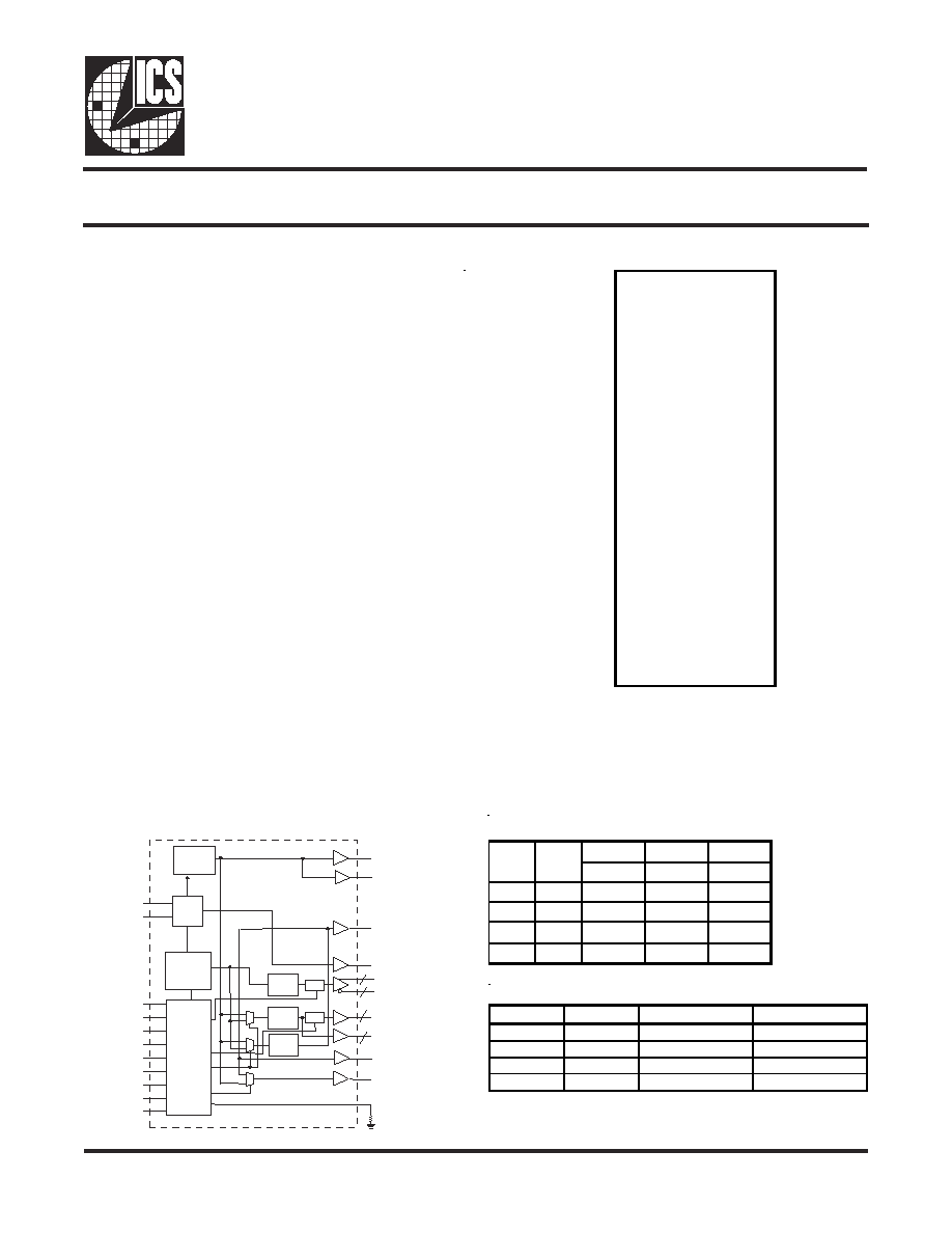
Block Diagram
Recommended Application:
CK-408 clock for Brookdale/Odem/Montara-GM for P4/Banias
processor.
Output Features:
∑
3 Differential CPU Clock Pairs @ 3.3V
∑
7 PCI (3.3V) @ 33.3MHz including 2 early PCI clocks
∑
3 PCI_F (3.3V) @ 33.3MHz
∑
1 USB (3.3V) @ 48MHz, 1 DOT (3.3V) @ 48MHz
∑
1 REF (3.3V) @ 14.318MHz
∑
5 3V66 (3.3V) @ 66.6MHz
∑
1 VCH/3V66 (3.3V) @ 48MHz or 66.6MHz
Features:
∑
Provides standard frequencies and additional 3%, 5%
and 10% over-clocked frequencies
∑
Supports spread spectrum modulation:
No spread, Center Spread (±0.3%, ±0.55%), or Down
Spread (-0.5%, -0.75%)
∑
Offers adjustable PCI early clock via latch inputs
∑
Selectable 1X or 2X strength for REF via I
2
C interface
∑
Programmable group to group skew
∑
Linear programmable frequency and spreading %
∑
Efficient power management scheme through PD#,
CPU_STOP# and PCI_STOP#.
∑
Uses external 14.318MHz crystal
∑
Stop clocks and functional control available through
I
2
C interface.
Key Specifications:
∑
CPU Output Jitter <150ps
∑
3V66 Output Jitter <250ps
∑
CPU Output Skew <100ps
Pin Configuration
Frequency Generator with 200MHz Differential CPU Clocks
ADVANCE INFORMATION documents contain information on products in the formative or design phase development. Characteristic data and other specifications are design goals.
ICS reserves the right to change or discontinue these products without notice. Third party brands and names are the property of their respective owners.
VDDREF
1
56 REF
X1
2
55 FS1
X2
3
54 FS0
GND
4
53 CPU_STOP#*
PCICLK_F0
5
52 CPUCLKT0
PCICLK_F1
6
51 CPUCLKC0
*ASEL/PCICLK_F2
7
50 VDDCPU
VDDPCI
8
49 CPUCLKT1
GND
9
48 CPUCLKC1
PCICLK0 10
47 GND
**E_PCICLK1/PCICLK1 11
46 VDDCPU
PCICLK2 12
45 CPUCLKT2
**E_PCICLK3/PCICLK3 13
44 CPUCLKC2
VDDPCI 14
43 MULTSEL*
GND 15
42 IREF
PCICLK4 16
41 GND
PCICLK5 17
40 PWRSAVE#*
PCICLK6 18
39 48MHz_USB/FS2
**
VDD3V66 19
38 48MHz_DOT
GND 20
37 VDD48
3V66_2 21
36 GND
3V66_3 22
35 3V66_1/VCH_CLK/FS3
**
3V66_4 23
34 PCI_STOP#*
3V66_5 24
33 3V66_0/FS4
**
*PD# 25
32 VDD3V66
VDDA 26
31 GND
GND 27
30 SCLK
Vtt_PWRGD# 28
29 SDATA
56-Pin 300mil SSOP
56-Pin 240mil TSSOP
*
These inputs have 120K internal pull-up resistors to VDD.
**
Internal pull-down resistors to ground.
I
C
S950813
Functionality Table
CPU
AGP
PCI
MHz
MHz
MHz
0
0
100.00
66.67
33.33
0
1
133.33
66.67
33.33
1
0
200.00
66.67
33.33
1
1
166.66
66.66
33.33
FS1
FS0
PLL2
PLL1
Spread
Spectrum
3V66 (5:2)
48MHz_USB
48MHz_DOT
X1
X2
XTAL
OSC
3V66
DIVDER
PD#
Vtt_PWRGD#
PWRSAVE#
CPU_STOP#
PCI_STOP#
MULTSEL
SDATA
SCLK
FS (4:0)
I REF
Control
Logic
Config.
Reg.
REF
3V66_0
CPU
DIVDER
3
3
CPUCLKT (2:0)
CPUCLKC (2:0)
Stop
3V66_1/VCH_CLK
PCICLK (6:0)
PCI
DIVDER
3
7
PCICLK_F (2:0)
Stop
Asynchronous AGP/PCI Frequency Selection Table
Byte7 Bit5 Byte7 Bit4
AGP Frequency
PCI Frequency
0
0
66.00
33.00
0
1
75.43
37.72
1
0
88.00
44.00
1
1
--
--
2
ICS950813
Advance Information
0708--10/10/02
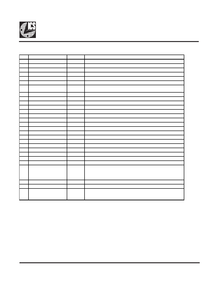
Pin Description
PIN # PIN NAME
PIN TYPE
DESCRIPTION
1
VDDREF
PWR
Ref, XTAL power supply, nominal 3.3V
2
X1
IN
Crystal input,nominally 14.318MHz.
3
X2
OUT
Crystal output, Nominally 14.318MHz
4
GND
PWR
Ground pin.
5
PCICLK_F0
OUT
Free running PCI clock not affected by PCI_STOP# .
6
PCICLK_F1
OUT
Free running PCI clock not affected by PCI_STOP# .
7
*ASEL/PCICLK_F2
I/O
Asynchronous AGP/PCI frequency latch input pin / 3.3V PCI free running
clock put. Pull-Up = Main PLL / Pull-Down = Async Fix PLL
8
VDDPCI
PWR
Power supply for PCI clocks, nominal 3.3V
9
GND
PWR
Ground pin.
10
PCICLK0
OUT
PCI clock output.
11
**E_PCICLK1/PCICLK1
I/O
Early/Normal PCI clock output latched at power up.
12
PCICLK2
OUT
PCI clock output.
13
**E_PCICLK3/PCICLK3
I/O
Early/Normal PCI clock output latched at power up.
14
VDDPCI
PWR
Power supply for PCI clocks, nominal 3.3V
15
GND
PWR
Ground pin.
16
PCICLK4
OUT
PCI clock output.
17
PCICLK5
OUT
PCI clock output.
18
PCICLK6
OUT
PCI clock output.
19
VDD3V66
PWR
Power pin for the 3V66 clocks.
20
GND
PWR
Ground pin.
21
3V66_2
OUT
3.3V 66.66MHz clock output
22
3V66_3
OUT
3.3V 66.66MHz clock output
23
3V66_4
OUT
3.3V 66.66MHz clock output
24
3V66_5
OUT
3.3V 66.66MHz clock output
25
*PD#
IN
Asynchronous active low input pin used to power down the device into a low
power state. The internal clocks are disabled and the VCO and the crystal
are stopped. The latency of the power down will not be greater than 3ms.
26
VDDA
PWR
3.3V power for the PLL core.
27
GND
PWR
Ground pin.
28
Vtt_PWRGD#
IN
This 3.3V LVTTL input is a level sensitive strobe used to determine when
latch inputs are valid and are ready to be sampled. This is an active low
input.
3
ICS950813
Advance Information
0708--10/10/02
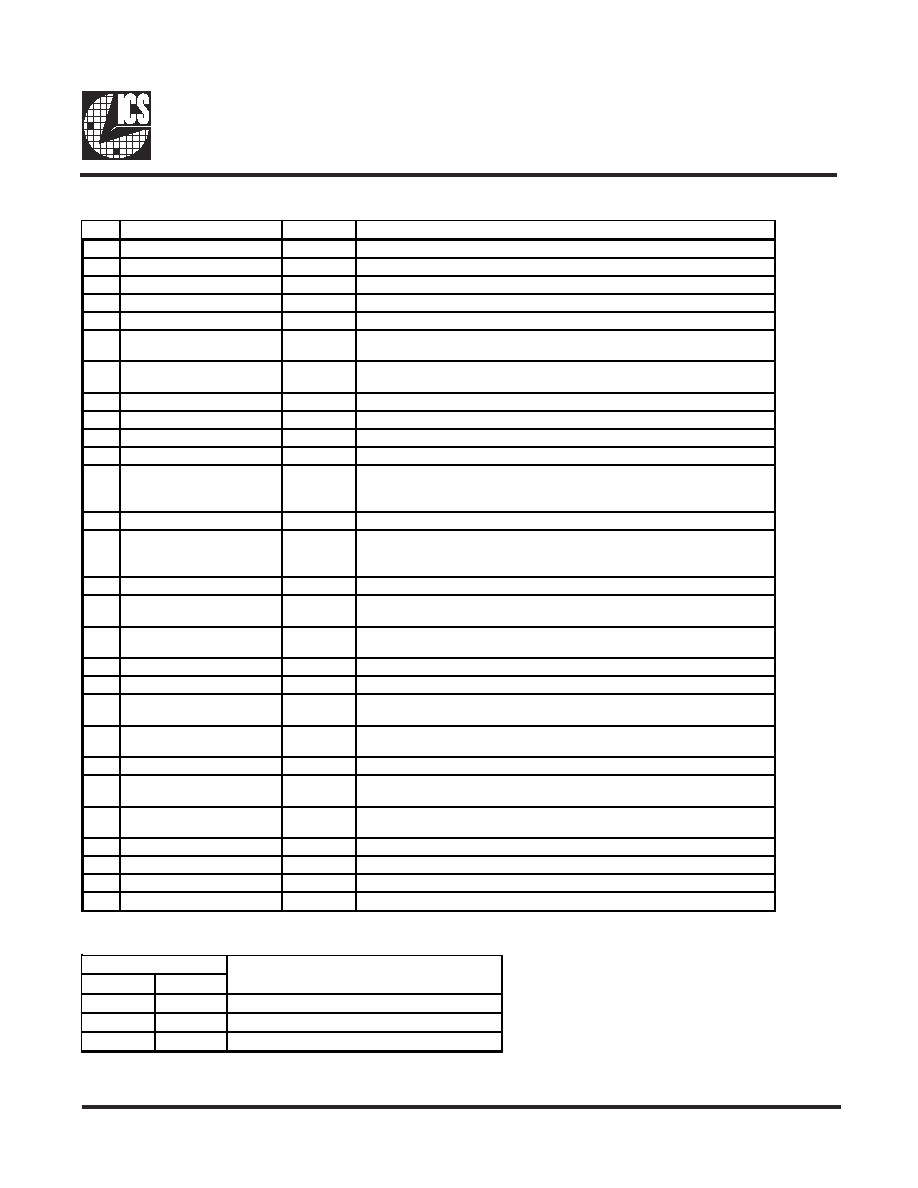
Pin Description (Continued)
PIN # PIN NAME
PIN TYPE
DESCRIPTION
29
SDATA
I/O
Data pin for I2C circuitry 5V tolerant
30
SCLK
IN
Clock pin of I2C circuitry 5V tolerant
31
GND
PWR
Ground pin.
32
VDD3V66
PWR
Power pin for the 3V66 clocks.
33
3V66_0/FS4**
I/O
Frequency select latch input pin / 3.3V 66.66MHz clock output.
34
PCI_STOP#*
IN
Stops all PCICLKs besides the PCICLK_F clocks at logic 0 level, when input
low
35
3V66_1/VCH_CLK/FS3**
I/O
Frequency select latch input pin / 3.3V 66.66MHz clock output / 48MHz
VCH clock output.
36
GND
PWR
Ground pin.
37
VDD48
PWR
Power for 24 & 48MHz output buffers and fixed PLL core.
38
48MHz_DOT
OUT
48MHz clock output.
39
48MHz_USB/FS2**
I/O
Frequency select latch input pin / 3.3V 48MHz clock output.
40
PWRSAVE#*
IN
Real Time input pin to change frequency to under-clock entries located in
FS 4:2 = '100'. Clock groups gear ratio will not be change during this
operation.
41
GND
PWR
Ground pin.
42
IREF
OUT
This pin establishes the reference current for the CPUCLK pairs. This pin
requires a fixed precision resistor tied to ground in order to establish the
appropriate current.
43
MULTSEL*
IN
3.3V LVTTL input for selection the current multiplier for CPU outputs
44
CPUCLKC2
OUT
"Complementary" clocks of differential pair CPU outputs. These are current
mode outputs. External resistors are required for voltage bias.
45
CPUCLKT2
OUT
"True" clocks of differential pair CPU outputs. These are current mode
outputs. External resistors are required for voltage bias.
46
VDDCPU
PWR
Supply for CPU clocks, 3.3V nominal
47
GND
PWR
Ground pin.
48
CPUCLKC1
OUT
"Complementary" clocks of differential pair CPU outputs. These are current
mode outputs. External resistors are required for voltage bias.
49
CPUCLKT1
OUT
"True" clocks of differential pair CPU outputs. These are current mode
outputs. External resistors are required for voltage bias.
50
VDDCPU
PWR
Supply for CPU clocks, 3.3V nominal
51
CPUCLKC0
OUT
"Complementary" clocks of differential pair CPU outputs. These are current
mode outputs. External resistors are required for voltage bias.
52
CPUCLKT0
OUT
"True" clocks of differential pair CPU outputs. These are current mode
outputs. External resistors are required for voltage bias.
53
CPU_STOP#*
IN
Stops all CPUCLK besides the free running clocks
54
FS0
IN
Frequency select pin.
55
FS1
IN
Frequency select pin.
56
REF
OUT
14.318 MHz reference clock.
Power Supply
VDD
GND
1
4
Xtal, Ref, CPU PLL, digital
37
36
48MHz, Fix Digital, Fix Analog
46
47
Master clock, CPU Analog
Pin Number
Description
4
ICS950813
Advance Information
0708--10/10/02
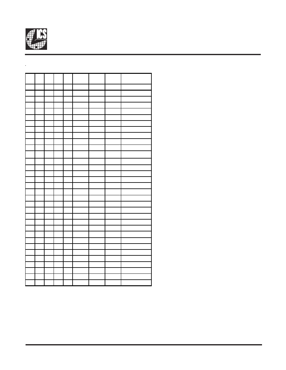
Frequency Select Table 1
Bit4 Bit3 Bit2 Bit1 Bit0
CPU
AGP
PCI
Spread
FS4 FS3 FS2 FS1 FS0
MHz
MHz
MHz
%
0
0
0
0
0
100.00
66.67
33.33
0.3% Center
0
0
0
0
1
133.33
66.67
33.33
0.3% Center
0
0
0
1
0
200.00
66.67
33.33
0.3% Center
0
0
0
1
1
166.66
66.66
33.33
0.3% Center
0
0
1
0
0
100.00
66.67
33.33
0 - 0.5% down
0
0
1
0
1
133.33
66.67
33.33
0 - 0.5% down
0
0
1
1
0
200.00
66.67
33.33
0 - 0.5% down
0
0
1
1
1
166.66
66.66
33.33
0 - 0.5% down
0
1
1
0
0
100.00
66.67
33.33
0.55% Center
0
1
1
0
1
133.33
66.67
33.33
0.55% Center
0
1
1
1
0
200.00
66.67
33.33
0.55% Center
0
1
1
1
1
166.66
66.66
33.33
0.55% Center
0
1
0
0
0
100.00
66.67
33.33
0 - 0.75% down
0
1
0
0
1
133.33
66.67
33.33
0 - 0.75% down
0
1
0
1
0
200.00
66.67
33.33
0 - 0.75% down
0
1
0
1
1
166.66
66.66
33.33
0 - 0.75% down
1
0
0
0
0
80.00
53.33
26.67
Spread Off
1
0
0
0
1
106.66
53.33
26.67
Spread Off
1
0
0
1
0
160.00
53.33
26.67
Spread Off
1
0
0
1
1
133.33
53.33
26.67
Spread Off
1
0
1
0
0
103.00
68.67
34.33
0.3% Center
1
0
1
0
1
137.33
68.66
34.33
0.3% Center
1
0
1
1
0
206.00
68.67
34.33
0.3% Center
1
0
1
1
1
171.66
68.66
34.33
0.3% Center
1
1
0
0
0
105.00
70.00
35.00
0.3% Center
1
1
0
0
1
140.00
70.00
35.00
0.3% Center
1
1
0
1
0
Tristate Tristate Tristate
N/A
1
1
0
1
1
174.99
70.00
35.00
0.3% Center
1
1
1
0
0
110.00
73.33
36.67
0.3% Center
1
1
1
0
1
146.66
73.33
36.67
0.3% Center
1
1
1
1
0
Test/2
Test/4
Test/8
N/A
1
1
1
1
1
183.33
73.33
36.67
0.3% Center
5
ICS950813
Advance Information
0708--10/10/02
Host Swing Select Functions
MULTSEL
0
1
Output
Ioh = 4 * I REF
Ioh = 6 * I REF
1.0V @ 50 ohm
0.7V @ 50 ohm
Voh @ Z
Board Target
Reference R,
Rr = 221 1%,
Iref = 5.00mA
Rr = 475 1%,
Iref = 2.32mA
50 ohms
50 ohms
PCI Select Functions
1
0
1.0ns
1
1
1.5ns
0
0
0ns
0
1
0.5ns
E_PCICLK1
E_PCICLK3
E_PCICLK(3,1)
*
Note:
*
Approximate values
E_PCICLK3 = 10Kohm resistor.
0 = No resistor
1 = 10Kohm pull-up to V
DD
.
E_PCICLK1 = 10Kohm resistor.
Frequency Select Table 2
FS4
FS3
FS2
0
0
0
0
0
1
0
1
0
0
1
1
1
0
0
1
0
1
1
1
0
1
1
1
Freqency Select
CPU, 3V66, PCI
Standard Clocking
10% Overclocking
Clocking Mode
Standard Clocking
0.3% Center Spread
Standard Clocking
0 to -0.5%, Down Spread
0.3% Center Spread
Standard Clocking
0 to - 0.75%, Down
Pwr Save Clocking
Spread Off
0.3% Center Spread
3% Overclocking
0.3% Center Spread
5% Overclocking
0.3% Center Spread
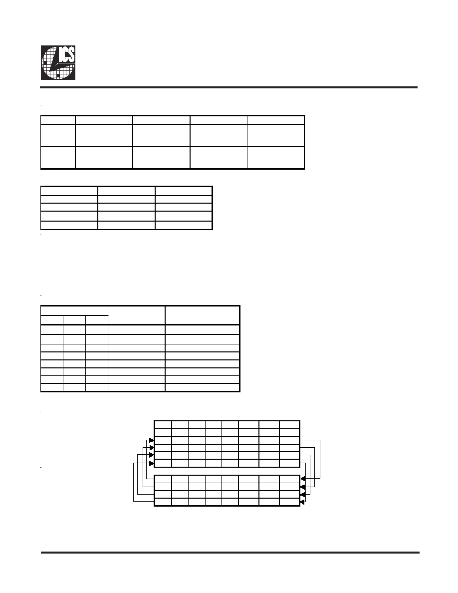
PWRSAVE# Usage Illustration
Bit4
Bit3
Bit2
Bit1
Bit0
CPU
AGP
PCI
FS4
FS3
FS2
FS1
FS0
MHz
MHz
MHz
X
X
X
0
0
XXX
XXX
XXX
X
X
X
0
1
XXX
XXX
XXX
X
X
X
1
0
XXX
XXX
XXX
X
X
X
1
1
XXX
XXX
XXX
1
0
0
0
0
80.00
53.33
26.67
1
0
0
0
1
106.66
53.33
26.67
1
0
0
1
0
160.00
53.33
26.67
1
0
0
1
1
133.33
53.33
26.67
PWRSAVE# = '0'. as
PWRSAVE# is driven to low '0'.
The output frequencies of the
CPU, AGP and PCI clock will
smoothly switch to frequencies
indicated by FS (4:2) = 100. The
frequencies gear ratio will be kept
the same. Notice that the 48MHz
& REF frequencies will not be
changed. This function can be
used with asynchronous
AGP/PCI frequencies.
PWRSAVE# = '1'. as
PWRSAVE# is driven back to
high '1'. The output frequencies
will be driven back to the
original programmed
frequencies smoothly. Notice
that this operation will only
happen after the PWRSAVE#
has been driven to '0'. This will
not affect power up or I2C
programmed frequencies if the
PWRSAFE# has been tied to a
'1'.