Integrated
Circuit
Systems, Inc.
ICS951402
Advance Information
0660--05/05/05
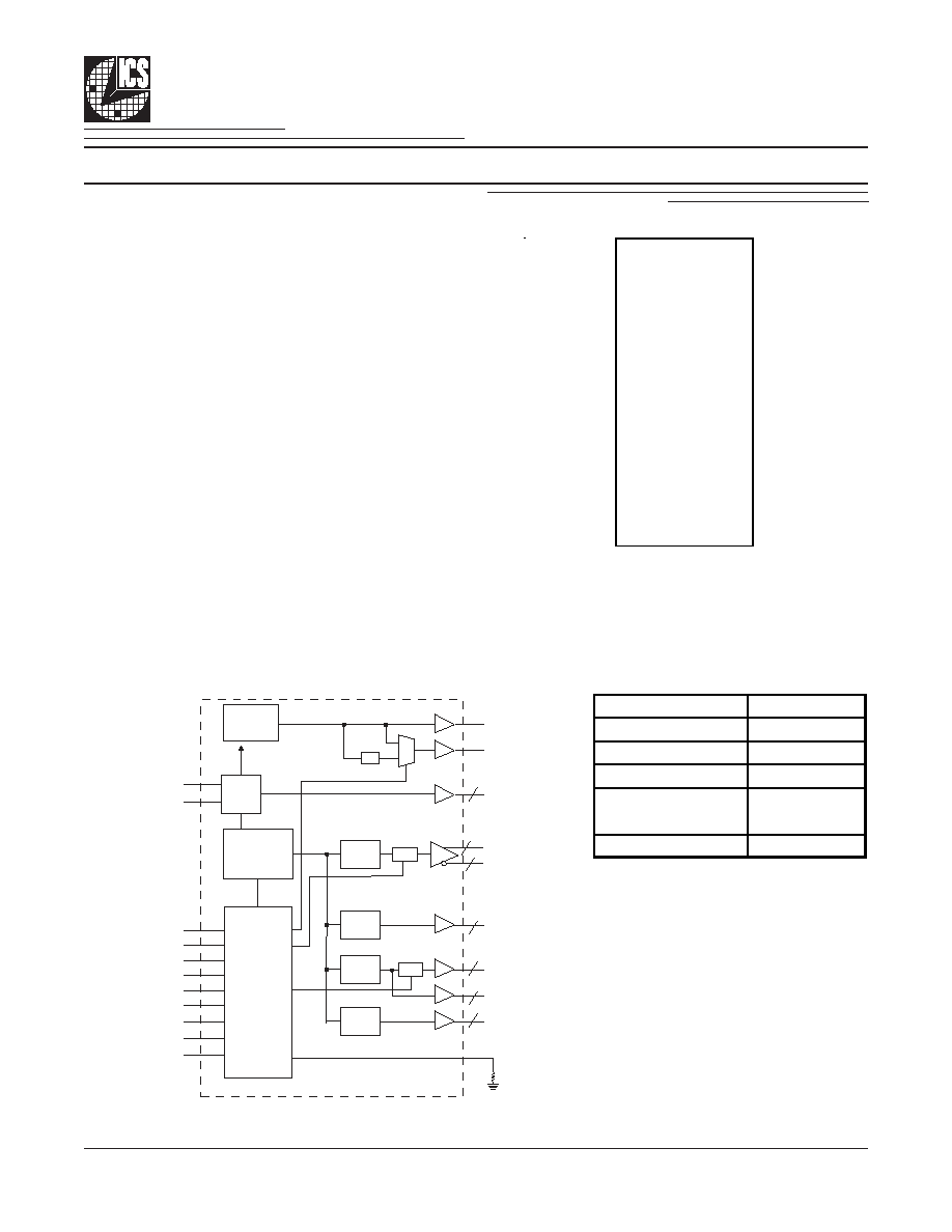
Block Diagram
Pin Configuration
Recommended Application:
ATI chipset, P4 system, Banias system
Output Features:
∑
2 - Pairs of differential CPUCLKs (differential current mode)
∑
1 - SDRAM @ 3.3V
∑
8 - PCI @3.3V (selectable 33/66 MHz) (2 free-running)
∑
2 - AGP @ 3.3V
∑
2- 48MHz, @3.3V fixed.
∑
1- 24/48MHz, @3.3V selectable by I
2
C
(Default is 24MHz)
∑
3- REF @3.3V, 14.318MHz.
Features/Benefits:
∑
Support for Intel Banias power management features
∑
Programmable output frequency, divider ratios, output rise/
falltime, output skew.
∑
Programmable spread percentage for EMI control.
∑
Watchdog timer technology to reset system
if system malfunctions.
∑
Programmable watch dog safe frequency.
∑
Support I
2
C Index read/write and block read/write
operations.
∑
Supports spread spectrum for EMI reduction; default is
spread spectrum ON.
Programmable Timing Control HubTM for P
4
TM processor
* These inputs have a 120K pull up to VDD.
** These inputs have a 120K pull down to GND.
ADVANCE INFORMATION documents contain information on products in the formative or design phase development. Characteristic data and other specifications are design goals.
ICS reserves the right to change or discontinue these products without notice. Third party brands and names are the property of their respective owners.
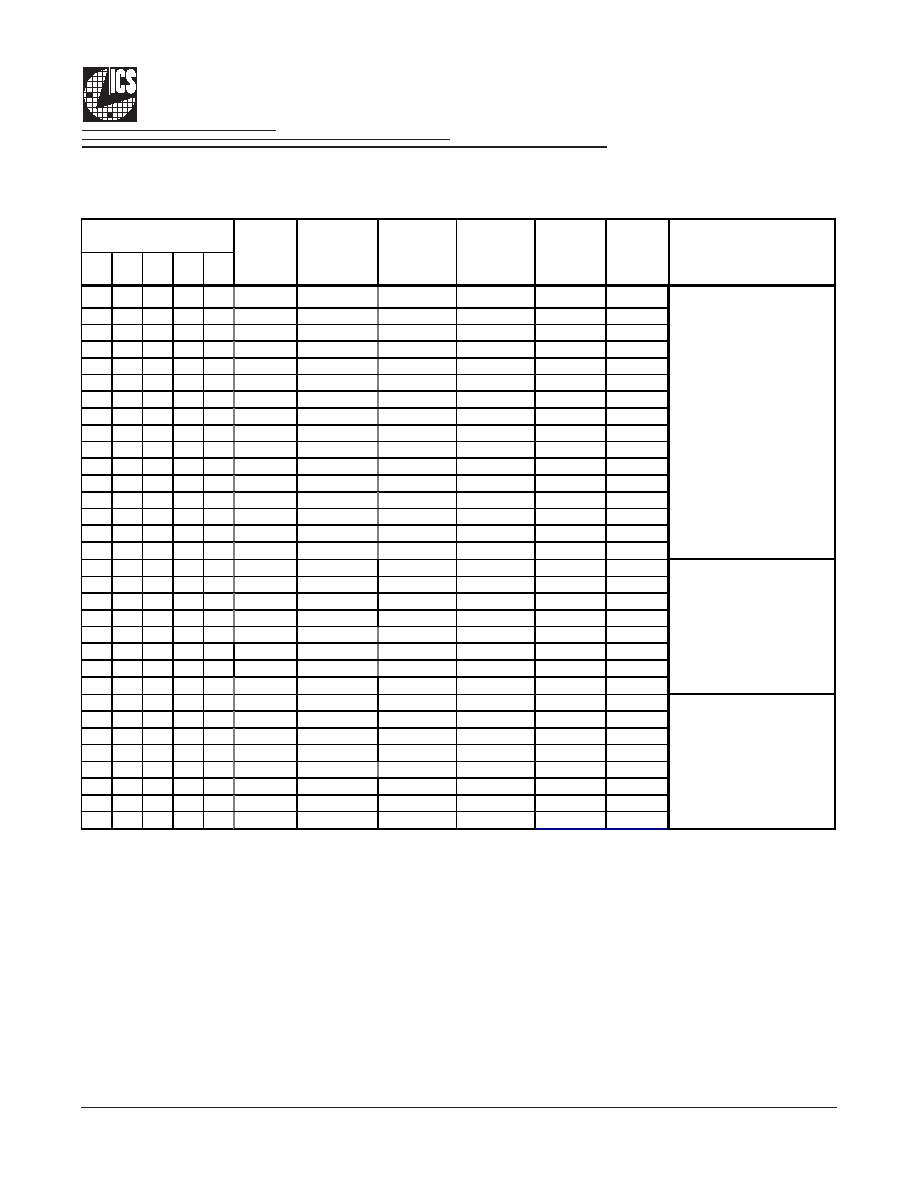
48-Pin TSSOP & SSOP
Power Groups
VDDCPU = CPU
VDDPCI = PCICLK_F, PCICLK
VDDSD = SDRAM
AVDD48 = 48MHz, 24MHz, fixed PLL
AVDD = Analog Core PLL
VDDAGP= AGP
VDDREF = Xtal, REF
Skew Requirements
VDDREF 1
48 VDDSDR
FS0/REF0 2
47 SDRAM_OUT
FS1/REF1 3
46 GNDSDR
FS2/REF2 4
45 CPU_STOP#*
GNDREF 5
44 CPUCLKT1
X1 6
43 CPUCLKC1
X2 7
42 VDDCPU
GND 8
41 GNDCPU
VDD 9
40 CPUCLKT0
*VttPWR_GD/PD# 10
39 CPUCLKC0
PCI66/33#_SEL 11
38 IREF
PCI_STOP#* 12
37 GND
VDDPCI 13
36 AVDD
FS3/PCICLK_F0 14
35 SCLK
FS4/PCICLK_F1 15
34 SDATA
PCICLK0 16
33 GNDAGP
PCICLK1 17
32 AGPCLK0
GNDPCI 18
31 AGPCLK1
VDDPCI 19
30 VDDAGP
PCICLK2 20
29 AVDD48
PCICLK3 21
28 48MHz_0
PCICLK4 22
27 48MHz_1
PCICLK5 23
26 24_48MHz/SEL24_48#MHz**
GNDPCI 24
25 GND48
I
C
S
9
514
02
PCI-PCI
<±350ps
AGP-AGP
<±350ps
CPU-AGP
<±500ps
CPU-PCI
<±500ps
CPU-SDRAM
<±1ns
AGP-PCI
AGP leading
<±1ns
I REF
CPU
DIVDER
PLL2
PLL1
Spread
Spectrum
48MHz (0:1)
24_48MHz
PCICLK (5:0)
AGP (1:0)
PCICLK_F (1:0)
2
2
1
6
3
X1
X2
XTAL
OSC
SDRAM
SDRAM_OUT
PCI
DIVDER
Stop
SDATA
SCLK
FS (4:0)
PD#
PCI_STOP#
CPU_STOP#
PD#/Vtt_PWRGD
PCI66/33#SEL
24_48SEL#
Control
Logic
Config.
Reg.
/ 2
REF (2:0)
AGP
DIVDER
Stop
2
2
CPUCLKT (1:0)
CPUCLKC (1:0)

2
Integrated
Circuit
Systems, Inc.
ICS951402
Advance Information
0660--05/05/05
Pin Description
PIN NUMBER
PIN NAME
TYPE
DESCRIPTION
1
VDDREF
PWR
Ref, XTAL power supply, nominal 3.3V
2
FS0/REF0
I/O
Frequency select latch input pin / 14.318 MHz reference clock.
3
FS1/REF1
I/O
Frequency select latch input pin / 14.318 MHz reference clock.
4
FS2/REF2
I/O
Frequency select latch input pin / 14.318 MHz reference clock.
5
GNDREF
PWR
Ground pin for the REF outputs.
6
X1
IN
Crystal input, Nominally 14.318MHz.
7
X2
OUT
Crystal output, Nominally 14.318MHz
8
GND
PWR
Ground pin.
9
VDD
PWR
Power supply, nominal 3.3V
10
*VttPWR_GD/PD#
IN
This 3.3V LVTTL input is a level sensitive strobe used to determine
when latch inputs are valid and are ready to be sampled. This is an
active high input. / Asynchronous active low input pin used to power
down the device into a low power state.
11
PCI66/33#_SEL
IN
Selects all PCI clock frequencies to be 33Mhz or 66Mhz. 0 = 33Mhz , 1
= 66Mhz
12
PCI_STOP#*
IN
Stops all PCICLKs besides the PCICLK_F clocks at logic 0 level, when
input low
13
VDDPCI
PWR
Power supply for PCI clocks, nominal 3.3V
14
FS3/PCICLK_F0
I/O
Frequency select latch input pin / 3.3V PCI free running clock output.
15
FS4/PCICLK_F1
I/O
Frequency select latch input pin / 3.3V PCI free running clock output.
16
PCICLK0
OUT
PCI clock output.
17
PCICLK1
OUT
PCI clock output.
18
GNDPCI
PWR
Ground pin for the PCI outputs
19
VDDPCI
PWR
Power supply for PCI clocks, nominal 3.3V
20
PCICLK2
OUT
PCI clock output.
21
PCICLK3
OUT
PCI clock output.
22
PCICLK4
OUT
PCI clock output.
23
PCICLK5
OUT
PCI clock output.
24
GNDPCI
PWR
Ground pin for the PCI outputs
25
GND48
PWR
Ground pin for the 48MHz outputs
26
24_48MHz/SEL24_48#MHz**
I/O
24/48MHz clock output / Latched select input for 24/48MHz output.
0=48MHz, 1 = 24MHz.
27
48MHz_1
OUT
48MHz clock output.
28
48MHz_0
OUT
48MHz clock output.
29
AVDD48
PWR
Analog power for 48MHz outputs and fixed PLL core, nominal 3.3V
30
VDDAGP
PWR
Power supply for AGP clocks, nominal 3.3V
31
AGPCLK1
OUT
AGP clock output
32
AGPCLK0
OUT
AGP clock output
33
GNDAGP
PWR
Ground pin for the AGP outputs
34
SDATA
I/O
Data pin for SMBus circuitry, 5V tolerant.
35
SCLK
IN
Clock pin of SMBus circuitry, 5V tolerant.
36
AVDD
PWR
3.3V Analog Power pin for Core PLL
37
GND
PWR
Ground pin.
38
IREF
OUT
This pin establishes the reference current for the differential current-
mode output pairs. This pin requires a fixed precision resistor tied to
ground in order to establish the appropriate current. 475 ohms is the
standard value.
39
CPUCLKC0
OUT
Complementary clock of differential pair CPU outputs. This clock is 180
degrees out of phase with the SDRAM clock.
40
CPUCLKT0
OUT
True clock of differential pair CPU outputs. This clock is in phase with
the SDRAM clock
41
GNDCPU
PWR
Ground pin for the CPU outputs
42
VDDCPU
PWR
Supply for CPU clocks, 3.3V nominal
43
CPUCLKC1
OUT
Complementary clock of differential pair CPU outputs. This clock is 180
degrees out of phase with the SDRAM clock.
44
CPUCLKT1
OUT
True clock of differential pair CPU outputs. This clock is in phase with
the SDRAM clock
45
CPU_STOP#*
IN
Stops all CPUCLK besides the free running clocks
46
GNDSDR
PWR
Ground pin for the SDRAM outputs.
47
SDRAM_OUT
OUT
SDRAM seed clock output for external buffer
48
VDDSDR
PWR
Supply for SDRAM clocks, nominal 3.3V.

4
Integrated
Circuit
Systems, Inc.
ICS951402
Advance Information
0660--05/05/05
*See notes on the following page
.
General I
2
C serial interface information for the ICS951402
How to Write:
∑ Controller (host) sends a start bit.
∑ Controller (host) sends the write address D2
(H)
∑ ICS clock will
acknowledge
∑ Controller (host) sends the begining byte location = N
∑ ICS clock will
acknowledge
∑ Controller (host) sends the data byte count = X
∑ ICS clock will
acknowledge
∑ Controller (host) starts sending
Byte N through
Byte N + X -1
(see Note 2)
∑ ICS clock will
acknowledge each byte one at a time
∑ Controller (host) sends a Stop bit
How to Read:
∑ Controller (host) will send start bit.
∑ Controller (host) sends the write address D2
(H)
∑ ICS clock will
acknowledge
∑ Controller (host) sends the begining byte
location = N
∑ ICS clock will
acknowledge
∑ Controller (host) will send a separate start bit.
∑ Controller (host) sends the read address D3
(H)
∑ ICS clock will
acknowledge
∑ ICS clock will send the data byte count = X
∑ ICS clock sends
Byte N + X -1
∑ ICS clock sends
Byte 0 through byte X (if X
(H)
was written to byte 8)
.
∑ Controller (host) will need to acknowledge each
byte
∑ Controllor (host) will send a not acknowledge bit
∑ Controller (host) will send a stop bit
ICS (Slave/Receiver)
T
WR
ACK
ACK
ACK
ACK
ACK
P
stoP bit
X Byt
e
Index Block Write Operation
Slave Address D2
(H)
Beginning Byte = N
WRite
starT bit
Controller (Host)
Byte N + X - 1
Data Byte Count = X
Beginning Byte N
T
starT bit
WR
WRite
RT
Repeat starT
RD
ReaD
Beginning Byte N
Byte N + X - 1
N
Not acknowledge
P
stoP bit
Slave Address D3
(H)
Index Block Read Operation
Slave Address D2
(H)
Beginning Byte = N
ACK
ACK
Data Byte Count = X
ACK
ICS (Slave/Receiver)
Controller (Host)
X Byt
e
ACK
ACK