Äîêóìåíòàöèÿ è îïèñàíèÿ www.docs.chipfind.ru
Integrated
Circuit
Systems, Inc.
ICS951412
0883G--12/08/04
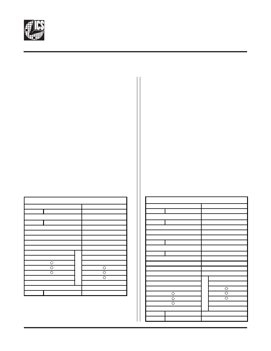
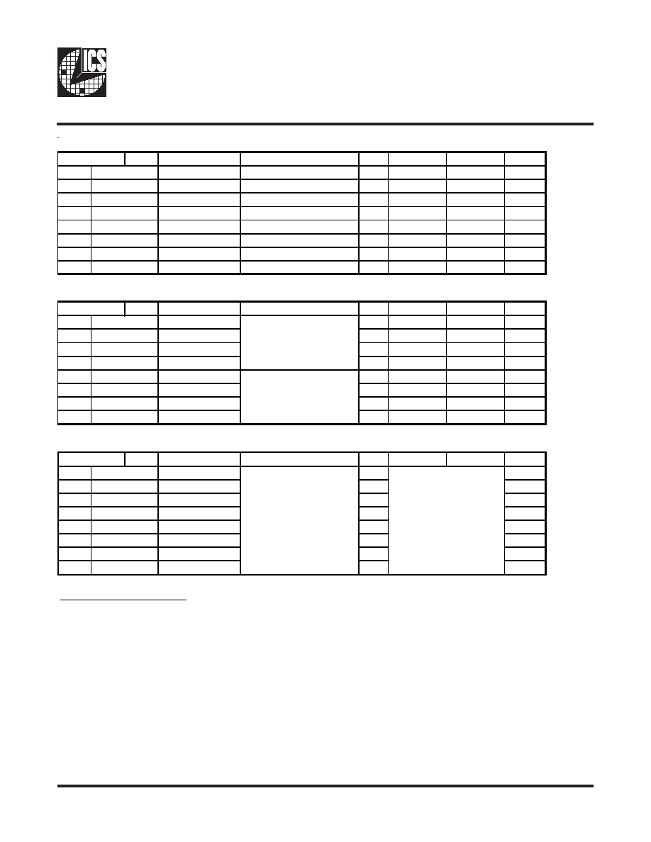
Functionality
Pin Configuration
Recommended Application:
ATI RS480 systems using AMD K8 processors
Output Features:
·
3 - 14.318 MHz REF clocks
·
1 - USB_48MHz USB clock
·
1 - HyperTransport 66 MHz clock seed
·
1 - PCI 33 MHz clock seed
·
2 - Pairs of AMD K8 clocks
·
6 - Pairs of SRC/PCI Express* clocks
·
2 - Pairs of ATIG (SRC/PCI Express) clocks
Features:
·
2 - Programmable Clock Request pins for SRC
clocks
·
Spread Spectrum for EMI reduction
·
Outputs may be disabled via SMBus
·
External crystal load capacitors for maximum
frequency accuracy
System Clock Chip for ATI RS480 K8-based Systems
CPU
HTT
PCI
MHz
MHz
MHz
0
0
0
Hi-Z
Hi-Z
Hi-Z
0
0
1
X
X/3
X/6
0
1
0
180.00
60.00
30.00
0
1
1
220.00
73.12
36.56
1
0
0
100.00
66.66
33.33
1
0
1
133.33
66.66
33.33
1
1
1
200.00
66.66
33.33
FS1
FS0
FS2
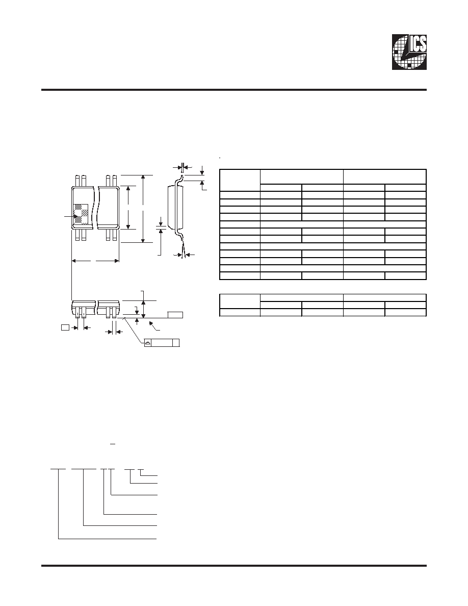
56 Pin SSOP/TSSOP
Power Groups
VDD
GND
56
55
Xtal, REF
51
49
PCICLK output
48
46
HTTCLK output
43
42
CPU Outputs
14, 21,
32,35
15, 20,
26,31,36
SRC outputs
39
38
Analog, CPU PLL
3
5
USB_48MHz output
Pin Number
Description
X1 1
56 VDDREF
X2 2
55 GND
VDD48 3
54 **FS0/REF0
USB_48MHz 4
53 **FS1/REF1
GND 5
52 REF2
NC 6
51 VDDPCI
SCLK 7
50 PCICLK0
SDATA 8
49 GNDPCI
**FS2 9
48 VDDHTT
**CLKREQA# 10
47 HTTCLK0
**CLKREQB# 11
46 GNDHTT
SRCCLKT7 12
45 CPUCLK8T0
SRCCLKC7 13
44 CPUCLK8C0
VDDSRC 14
43 VDDCPU
GNDSRC 15
42 GNDCPU
SRCCLKT6 16
41 CPUCLK8T1
SRCCLKC6 17
40 CPUCLK8C1
SRCCLKT5 18
39 VDDA
SRCCLKC5 19
38 GNDA
GNDSRC 20
37 IREF
VDDSRC 21
36 GNDSRC
SRCCLKT4 22
35 VDDSRC
SRCCLKC4 23
34 SRCCLKT0
SRCCLKT3 24
33 SRCCLKC0
SRCCLKC3 25
32 VDDATI
GNDSRC 26
31 GNDATI
ATIGCLKT1 27
30 ATIGCLKT0
ATIGCLKC1 28
29 ATIGCLKC0
Note: Pins preceeded by '**' have a 120 Kohm Internal Pull Down resistor
I
C
S951
41
2
*Other names and brands may be claimed as the property of others.
2
ICS951412
0883G--12/08/04
Pin Descriptions
PIN
#
PIN NAME
PIN
TYPE
DESCRIPTION
1
X1
IN
Crystal input, Nominally 14.318MHz.
2
X2
OUT
Crystal output, Nominally 14.318MHz
3
VDD48
PWR
Power pin for the 48MHz output.3.3V
4
USB_48MHz
OUT
48.00MHz USB clock
5
GND
PWR
Ground pin.
6
NC
N/A
No Connection.
7
SCLK
IN
Clock pin of SMBus circuitry, 5V tolerant.
8
SDATA
I/O
Data pin for SMBus circuitry, 5V tolerant.
9
**FS2
IN
Frequency select pin.
10
**CLKREQA#
IN
Output enable for PCI Express (SRC) outputs. SMBus selects which
outputs are controlled.
0 = enabled, 1 = tri-stated
11
**CLKREQB#
IN
Output enable for PCI Express (SRC) outputs. SMBus selects which
outputs are controlled.
0 = enabled, 1 = tri-stated
12
SRCCLKT7
OUT
True clock of differential SRC clock pair.
13
SRCCLKC7
OUT
Complement clock of differential SRC clock pair.
14
VDDSRC
PWR
Supply for SRC clocks, 3.3V nominal
15
GNDSRC
PWR
Ground pin for the SRC outputs
16
SRCCLKT6
OUT
True clock of differential SRC clock pair.
17
SRCCLKC6
OUT
Complement clock of differential SRC clock pair.
18
SRCCLKT5
OUT
True clock of differential SRC clock pair.
19
SRCCLKC5
OUT
Complement clock of differential SRC clock pair.
20
GNDSRC
PWR
Ground pin for the SRC outputs
21
VDDSRC
PWR
Supply for SRC clocks, 3.3V nominal
22
SRCCLKT4
OUT
True clock of differential SRC clock pair.
23
SRCCLKC4
OUT
Complement clock of differential SRC clock pair.
24
SRCCLKT3
OUT
True clock of differential SRC clock pair.
25
SRCCLKC3
OUT
Complement clock of differential SRC clock pair.
26
GNDSRC
PWR
Ground pin for the SRC outputs
27
ATIGCLKT1
OUT
True clock of differential SRC clock pair.
28
ATIGCLKC1
OUT
Complementary clock of differential SRC clock pair.
3
ICS951412
0883G--12/08/04
PIN
#
PIN NAME
TYPE
DESCRIPTION
29
ATIGCLKC0
OUT
Complementary clock of differential SRC clock pair.
30
ATIGCLKT0
OUT
True clock of differential SRC clock pair.
31
GNDATI
PWR
Ground for ATI Gclocks, nominal 3.3V
32
VDDATI
PWR
Power supply ATI Gclocks, nominal 3.3V
33
SRCCLKC0
OUT
Complement clock of differential SRC clock pair.
34
SRCCLKT0
OUT
True clock of differential SRC clock pair.
35
VDDSRC
PWR
Supply for SRC clocks, 3.3V nominal
36
GNDSRC
PWR
Ground pin for the SRC outputs
37
IREF
OUT
This pin establishes the reference current for the differential current-mode
output pairs. This pin requires a fixed precision resistor tied to ground in
order to establish the appropriate current. 475 ohms is the standard value.
38
GNDA
PWR
Ground pin for the PLL core.
39
VDDA
PWR
3.3V power for the PLL core.
40
CPUCLK8C1
OUT
Complementary clock of differential 3.3V push-pull K8 pair.
41
CPUCLK8T1
OUT
True clock of differential 3.3V push-pull K8 pair.
42
GNDCPU
PWR
Ground pin for the CPU outputs
43
VDDCPU
PWR
Supply for CPU clocks, 3.3V nominal
44
CPUCLK8C0
OUT
Complementary clock of differential 3.3V push-pull K8 pair.
45
CPUCLK8T0
OUT
True clock of differential 3.3V push-pull K8 pair.
46
GNDHTT
PWR
Ground pin for the HTT outputs
47
HTTCLK0
OUT
3.3V Hyper Transport output
48
VDDHTT
PWR
Supply for HTT clocks, nominal 3.3V.
49
GNDPCI
PWR
Ground pin for the PCI outputs
50
PCICLK0
OUT
PCI clock output.
51
VDDPCI
PWR
Power supply for PCI clocks, nominal 3.3V
52
REF2
OUT
14.318 MHz reference clock.
53
**FS1/REF1
I/O
Frequency select latch input pin / 14.318 MHz reference clock.
54
**FS0/REF0
I/O
Frequency select latch input pin / 14.318 MHz reference clock.
55
GND
PWR
Ground pin.
56
VDDREF
PWR
Ref, XTAL power supply, nominal 3.3V
Pin Descriptions (Continued)
4
ICS951412
0883G--12/08/04
General Description
The ICS951412 is a main clock synthesizer chip that provides all clocks required for ATI RS480-based systems.
An SMBus interface allows full control of the device.
Skew Characteristics
Parameter
Description
Test Conditons
Skew
Window
Unit
T
sk_CPU_CPU
measured at x-ing of CPU,
250
ps
T
sk_CPU_PCI
measured at x-ing of CPU,
1.5V of PCI clock
2000
ps
T
sk_PCI_PCI
measured between rising
edge at 1.5V
500
ps
T
sk_PCI33-HT66
measured between rising
edge at 1.5V
500
ps
T
sk_CPU_HT66
measured between rising
edge at 1.5V
2000
ps
T
sk_CPU_HT66
measured at x-ing of CPU,
1.5V of PCI clock
500
ps
T
sk_CPU_CPU
measured at x-ing of CPU,
200
ps
T
sk_CPU_PCI
measured at x-ing of CPU,
1.5V of PCI clock
200
ps
T
sk_PCI_PCI
measured between rising
edge at 1.5V
200
ps
T
sk_PCI33-HT66
measured between rising
edge at 1.5V
200
ps
T
sk_CPU_HT66
measured between rising
edge at 1.5V
200
ps
T
sk_CPU_HT66
measured at x-ing of CPU,
1.5V of PCI clock
200
ps
time independent
skew
not dependent on
V, T changes
time variant skew
varies over
V, T changes
Block Diagram
MAIN PLL
PCICLK0
CONTROL
LOGIC
XTAL
OSC.
CPUCLK8(1:0)
FIXED PLL
USB_48MHz
DIVIDER
DIVIDERS
REF(2:0)
HTTCLK0
SRCCLK(7:3,0)
CLKREQA#
SDATA
SCLK
FS(2:0)
CLKREQB#
SEL75#/100
X1
X2
IREF
ATIGCLK(1:0)
5
ICS951412
0883G--12/08/04
General SMBus serial interface information
How to Write:
· Controller (host) sends a start bit.
· Controller (host) sends the write address D2
(H)
· ICS clock will
acknowledge
· Controller (host) sends the begining byte location = N
· ICS clock will
acknowledge
· Controller (host) sends the data byte count = X
· ICS clock will
acknowledge
· Controller (host) starts sending
Byte N through
Byte N + X -1
(see Note 2)
· ICS clock will
acknowledge each byte one at a time
· Controller (host) sends a Stop bit
How to Read:
· Controller (host) will send start bit.
· Controller (host) sends the write address D2
(H)
· ICS clock will
acknowledge
· Controller (host) sends the begining byte
location = N
· ICS clock will
acknowledge
· Controller (host) will send a separate start bit.
· Controller (host) sends the read address D3
(H)
· ICS clock will
acknowledge
· ICS clock will send the data byte count = X
· ICS clock sends
Byte N + X -1
· ICS clock sends
Byte 0 through byte X (if X
(H)
was written to byte 8)
.
· Controller (host) will need to acknowledge each byte
· Controllor (host) will send a not acknowledge bit
· Controller (host) will send a stop bit
ICS (Slave/Receiver)
T
WR
ACK
ACK
ACK
ACK
ACK
P
stoP bit
X Byt
e
Index Block Write Operation
Slave Address D2
(H)
Beginning Byte = N
WRite
starT bit
Controller (Host)
Byte N + X - 1
Data Byte Count = X
Beginning Byte N
T
starT bit
WR
WRite
RT
Repeat starT
RD
ReaD
Beginning Byte N
Byte N + X - 1
N
Not acknowledge
P
stoP bit
Slave Address D3
(H)
Index Block Read Operation
Slave Address D2
(H)
Beginning Byte = N
ACK
ACK
Data Byte Count = X
ACK
ICS (Slave/Receiver)
Controller (Host)
X Byt
e
ACK
ACK
6
ICS951412
0883G--12/08/04
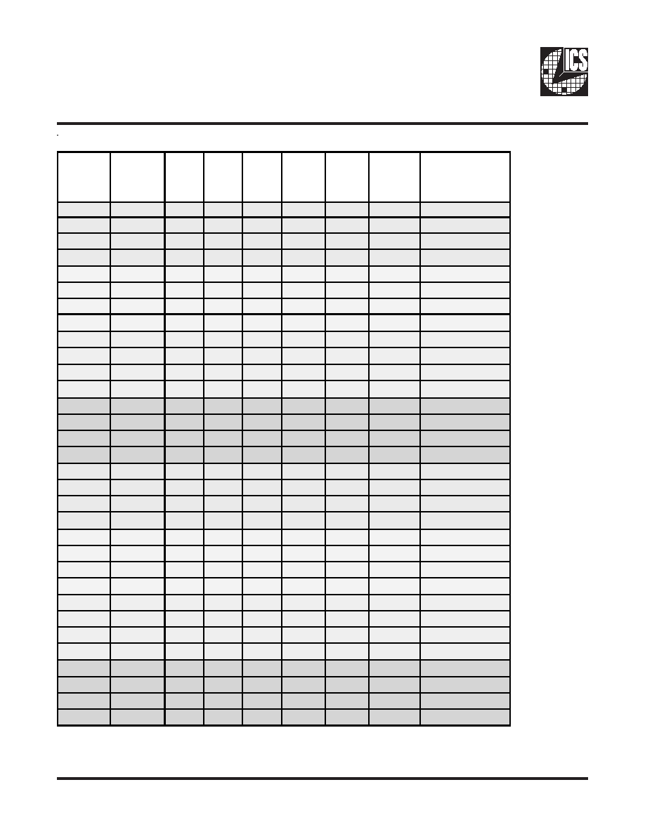
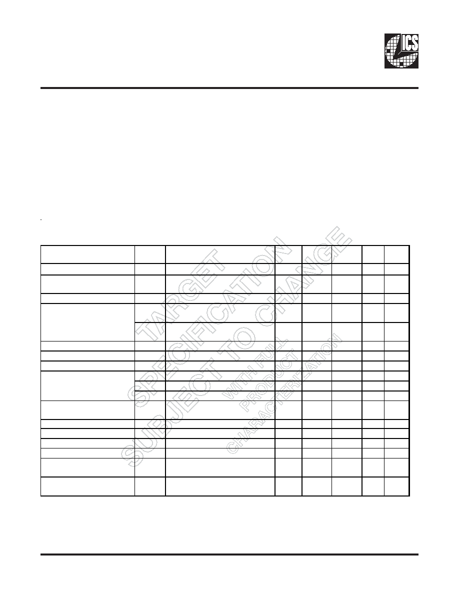
Table1: CPU Frequency Selection Table
CPU
FS4
(B0:b4)
CPU
FS3
(B0:b3)
Bit2
FS2
Bit1
FS1
Bit0
FS0
CPU
(MHz)
HTT66
(MHz)
PCI33
(MHz)
Spread
%
0
0
0
0
0
Hi-Z
Hi-Z
Hi-Z
None
0
0
0
0
1
X/6
X/12
X/24
None
0
0
0
1
0
180.00 60.00
30.00
None
0
0
0
1
1
220.00 73.33
36.67
None
0
0
1
0
0
100.00 66.67
33.33
None
0
0
1
0
1
133.33 66.67
33.33
None
0
0
1
1
0
166.67 66.67
33.33
None
0
0
1
1
1
200.00 66.67
33.33
None
0
1
0
0
0
186.00 62.00
31.00
None
0
1
0
0
1
214.00 71.33
35.67
None
0
1
0
1
0
190.00 63.33
31.67
None
0
1
0
1
1
210.00 70.00
35.00
None
0
1
1
0
0
102.00 68.00
34.00
None
0
1
1
0
1
136.00 68.00
34.00
None
0
1
1
1
0
170.00 68.00
34.00
None
0
1
1
1
1
204.00 68.00
34.00
None
1
0
0
0
0
169.58 56.53
28.26
-0.5%
1
0
0
0
1
229.43 76.48
38.24
-0.5%
1
0
0
1
0
179.55 59.85
29.93
-0.5%
1
0
0
1
1
219.45 73.15
36.58
-0.5%
1
0
1
0
0
99.75
66.50
33.25
-0.5%
1
0
1
0
1
133.00 66.50
33.25
-0.5%
1
0
1
1
0
166.25 66.50
33.25
-0.5%
1
0
1
1
1
199.50 66.50
33.25
-0.5%
1
1
0
0
0
185.54 61.85
30.92
-0.5%
1
1
0
0
1
106.73 71.16
35.58
-0.5%
1
1
0
1
0
189.53 63.18
31.59
-0.5%
1
1
0
1
1
209.48 69.83
34.91
-0.5%
1
1
1
0
0
101.75 67.83
33.92
-0.5%
1
1
1
0
1
135.66 67.83
33.91
-0.5%
1
1
1
1
0
169.58 67.83
33.92
-0.5%
1
1
1
1
1
203.49 67.83
33.92
-0.5%
7
ICS951412
0883G--12/08/04
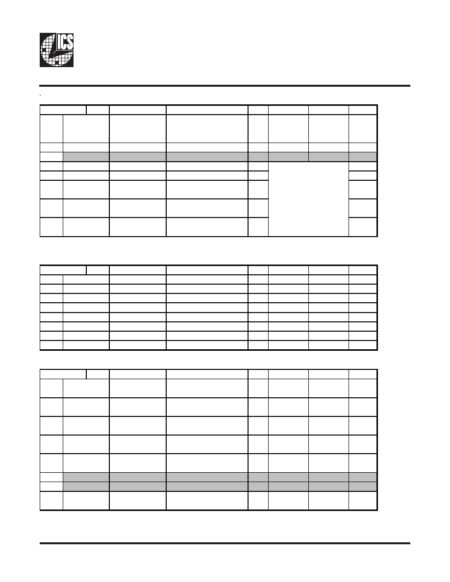
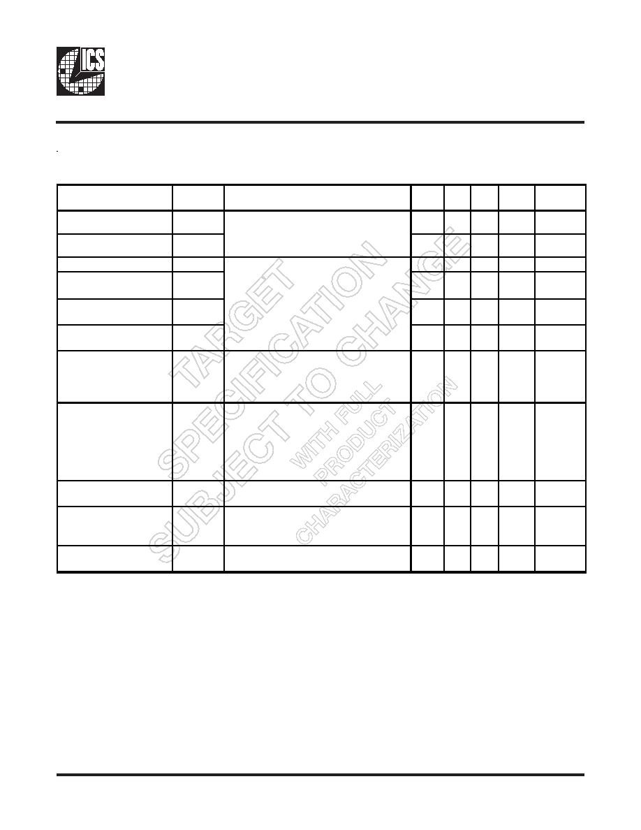
SMBus Table: Frequency Select Register
Pin #
Name
Control Function
Type
0
1
PWD
Bit 7
FS Source
Latched Input or SMBus
Frequency Select
RW
Latched
Inputs
SMBus
0
Bit 6
SS_EN
PLL Spread Enable
RW
OFF
ON
0
Bit 5
Reserved
Reserved
RW
Reserved
Reserved
X
Bit 4
FS4
Freq Select Bit 4
RW
0
Bit 3
FS3
Freq Select Bit 3
RW
0
Bit 2
FS2
Freq Select Bit 2
RW
Latched
Bit 1
FS1
Freq Select Bit 1
RW
Latched
Bit 0
FS0
Freq Select Bit 0
RW
Latched
Note: Byte 0 Bit 6, Byte 0 Bit 4 and Byte 5 Bit 4 must be set to '1' to fully enable spread.
SMBus Table: Output Control Register
Pin #
Name
Control Function
Type
0
1
PWD
Bit 7
PCICLK0
Output Enable
RW
Disable
Enable
1
Bit 6
HTTCLK0
Output Enable
RW
Disable
Enable
1
Bit 5
USB_48MHz
Output Enable
RW
Disable
Enable
1
Bit 4
REF0
Output Enable
RW
Disable
Enable
1
Bit 3
REF1
Output Enable
RW
Disable
Enable
1
Bit 2
REF2
Output Enable
RW
Disable
Enable
1
Bit 1
CPUCLK8(0)
Output Enable
RW
Disable
Enable
1
Bit 0
CPUCLK8(1)
Output Enable
RW
Disable
Enable
1
SMBus Table: CLKREQB# Output Control Register
Pin #
Name
Control Function
Type
0
1
PWD
Bit 7
REQBSRC7
CLKREQB# Controls
SRC7
RW
Does not
control
Controls
0
Bit 6
REQBSRC6
CLKREQB# Controls
SRC6
RW
Does not
control
Controls
0
Bit 5
REQBSRC5
CLKREQB# Controls
SRC5
RW
Does not
control
Controls
0
Bit 4
REQBSRC4
CLKREQB# Controls
SRC4
RW
Does not
control
Controls
0
Bit 3
REQBSRC3
CLKREQB# Controls
SRC3
RW
Does not
control
Controls
0
Bit 2
Reserved
Reserved
RW
Reserved
Reserved
X
Bit 1
Reserved
Reserved
RW
Reserved
Reserved
X
Bit 0
REQBSRC0
CLKREQB# Controls
SRC0
RW
Does not
control
Controls
0
34,33
22,23
24,25
-
-
Byte 2
12,13
16,17
18,19
See Table 1: CPU
Frequency Selection
Byte 0
-
-
-
-
-
-
-
-
4
50
Byte 1
47
54
45,44
41,40
53
52
8
ICS951412
0883G--12/08/04
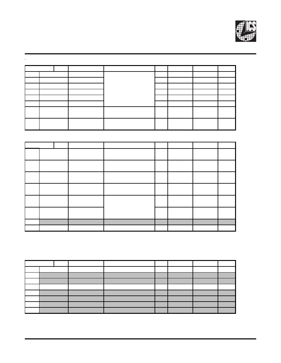
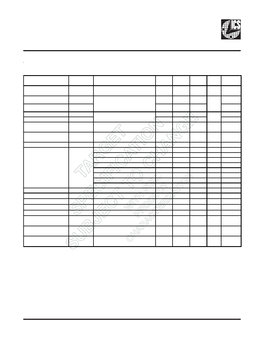
SMBus Table: SRCCLK(7:3,0), CLKREQA# Output Control Register
Pin #
Name
Control Function
Type
0
1
PWD
Bit 7
SRCCLK7
RW
Disable
Enable
1
Bit 6
SRCCLK6
RW
Disable
Enable
1
Bit 5
SRCCLK5
RW
Disable
Enable
1
Bit 4
SRCCLK4
RW
Disable
Enable
1
Bit 3
SRCCLK3
RW
Disable
Enable
1
Bit 2
SRCCLK0
RW
Disable
Enable
1
Bit 1
REQASRC3
CLKREQA# Controls
SRC3
RW
Does not
control
Controls
0
Bit 0
REQASRC0
CLKREQA# Controls
SRC0
RW
Does not
control
Controls
0
SMBus Table: SRCCLK(3,0), ATIGCLK Output Control Register
Pin #
Name
Control Function
Type
0
1
PWD
Bit 7
REQASRC7
CLKREQA# Controls
SRC7
RW
Does not
control
Controls
0
Bit 6
REQASRC6
CLKREQA# Controls
SRC6
RW
Does not
control
Controls
0
Bit 5
REQASRC5
CLKREQA# Controls
SRC5
RW
Does not
control
Controls
0
Bit 4
REQASRC4
CLKREQA# Controls
SRC4
RW
Does not
control
Controls
0
Bit 3
ATIGCLK1
RW
Disabled
Enabled
1
Bit 2
ATIGCLK0
RW
Disabled
Enabled
1
Bit 1
Reserved
Reserved
RW
Reserved
Reserved
0
Bit 0
USB_48Str
48MHz Strength Control
RW
1X
2X
0
Note: Do NOT simultaneously select CLKREQA# and CLKREQB# to control an SRC output.
Behavior of the device is undefined under these conditions.
SMBus Table: Output Drive and ATIG Frequency Control Register
Pin #
Name
Control Function
Type
0
1
PWD
Bit 7
REF2Str
REF2 Strength Control
RW
1X
2X
0
Bit 6
Reserved
Reserved
RW
Reserved
Reserved
0
Bit 5
Reserved
Reserved
RW
Reserved
Reserved
0
Bit 4
SRC SSEN
SRC Spread Enable
RW
Disable
Enable
0
Bit 3
Reserved
Reserved
RW
Reserved
Reserved
0
Bit 2
Reserved
Reserved
RW
Reserved
Reserved
0
Bit 1
Reserved
Reserved
RW
Reserved
Reserved
0
Bit 0
Reserved
Reserved
RW
Reserved
Reserved
0
-
-
-
Byte 5
52
-
-
-
-
Output Enable
These outputs cannot be
controlled by CLKREQ#
pins.
30,29
-
4
16,17
18,19
22,23
27,28
24,25
34,33
Byte 4
12,13
Byte 3
12,13
Master Output control.
Enables or disables
output, regardless of
CLKREQ# inputs.
16,17
18,19
22,23
24,25
34,33
9
ICS951412
0883G--12/08/04
SMBus Table: Device ID Register
Pin #
Name
Control Function
Type
0
1
PWD
Bit 7
DevID 7
Device ID MSB
R
-
-
0
Bit 6
DevID 6
Device ID 6
R
-
-
0
Bit 5
DevID 5
Device ID 5
R
-
-
0
Bit 4
DevID 4
Device ID4
R
-
-
1
Bit 3
DevID 3
Device ID3
R
-
-
0
Bit 2
DevID 2
Device ID2
R
-
-
0
Bit 1
DevID 1
Device ID1
R
-
-
1
Bit 0
DevID 0
Device ID LSB
R
-
-
0
SMBus Table: Vendor ID Register
Pin #
Name
Control Function
Type
0
1
PWD
Bit 7
RID3
R
-
-
X
Bit 6
RID2
R
-
-
X
Bit 5
RID1
R
-
-
X
Bit 4
RID0
R
-
-
X
Bit 3
VID3
R
-
-
0
Bit 2
VID2
R
-
-
0
Bit 1
VID1
R
-
-
0
Bit 0
VID0
R
-
-
1
SMBus Table: Byte Count Register
Pin #
Name
Control Function
Type
0
1
PWD
Bit 7
BC7
RW
0
Bit 6
BC6
RW
0
Bit 5
BC5
RW
0
Bit 4
BC4
RW
0
Bit 3
BC3
RW
1
Bit 2
BC2
RW
0
Bit 1
BC1
RW
0
Bit 0
BC0
RW
1
Bytes 9 to 21 are reserved
Byte 6
-
-
-
Writing to this register
will configure how many
bytes will be read back,
default is 9 bytes.
-
-
-
-
-
-
-
-
Revision ID
-
-
VENDOR ID
(0001 = ICS)
-
Byte Count
Programming b(7:0)
-
-
Byte 8
-
-
-
-
Byte 7
-
-
-
-
10
ICS951412
0883G--12/08/04
Absolute Maximum Ratings
Supply Voltage . . . . . . . . . . . . . . . . . . . . . . . . . 3.8V
Logic Inputs . . . . . . . . . . . . . . . . . . . . . . . . . . . GND 0.5 V to V
DD
+3.8 V
Ambient Operating Temperature . . . . . . . . . . 0°C to +70°C
Storage Temperature . . . . . . . . . . . . . . . . . . . . 65°C to +150°C
ESD Protection . . . . . . . . . . . . . . . . . . . . . . . . Input ESD protection usung human body model > 1KV
Stresses above those listed under
Absolute Maximum Ratings may cause permanent damage to the device. These
ratings are stress specifications only and functional operation of the device at these or any other conditions above those
listed in the operational sections of the specifications is not implied. Exposure to absolute maximum rating conditions
for extended periods may affect product reliability.
Electrical Characteristics - Input/Supply/Common Output Parameters
T
A
= 0 - 70°C; Supply Voltage V
DD
= 3.3 V +/-5%
PARAMETER
SYMBOL
CONDITIONS
MIN
TYP
MAX
UNITS NOTES
Input High Voltage
V
IH
3.3 V +/-5%
2
V
DD
+ 0.3
V
1
Input Low Voltage
V
IL
3.3 V +/-5%
V
SS
- 0.3
0.8
V
1
Input High Current
I
IH
V
IN
= V
DD
-5
5
uA
1
I
IL1
V
IN
= 0 V; Inputs with no pull-up
resistors
-5
uA
1
I
IL2
V
IN
= 0 V; Inputs with pull-up
resistors
-200
uA
1
Operating Current
I
DD3.3OP
all outputs driven
300
mA
Input Frequency
3
F
i
V
DD
= 3.3 V
14.31818
MHz
3
Pin Inductance
1
L
pin
7
nH
1
C
IN
Logic Inputs
5
pF
1
C
OUT
Output pin capacitance
6
pF
1
C
INX
X1 & X2 pins
5
pF
1
Clk Stabilization
1,2
T
STAB
From V
DD
Power-Up or de-assertion
of PD# to 1st clock
3
ms
1,2
Modulation Frequency
Triangular Modulation
30
33
kHz
1
SMBus Voltage
V
DD
2.7
5.5
V
1
Low-level Output Voltage
V
OL
@ I
PULLUP
0.4
V
1
Current sinking at V
OL
= 0.4 V
I
PULLUP
4
mA
1
SCLK/SDATA
Clock/Data Rise Time
3
T
RI2C
(Max VIL - 0.15) to (Min VIH + 0.15)
1000
ns
1
SCLK/SDATA
Clock/Data Fall Time
3
T
FI2C
(Min VIH + 0.15) to (Max VIL - 0.15)
300
ns
1
1
Guaranteed by design and characterization, not 100% tested in production.
2
See timing diagrams for timing requirements.
3
Input frequency should be measured at the REFOUT pin and tuned to ideal 14.31818MHz to meet
ppm frequency accuracy on PLL outputs.
Input Low Current
Input Capacitance
1
11
ICS951412
0883G--12/08/04
Electrical Characteristics - K8 Push Pull Differential Pair
T
A
= 0 - 70°C; V
DD
= 3.3 V +/-5%; C
L
=AMD64 Processor Test Load
PARAMETER
SYMBOL
CONDITIONS
MIN
TYP MAX UNITS
NOTES
Rising Edge Rate
V/t
2
10
V/ns
1
Falling Edge Rate
V/t
2
10
V/ns
1
Differential Voltage
V
DIFF
0.4
1.25
2.3
V
1
Change in V
DIFF_DC
Magnitude
V
DIFF
-150
150
mV
1
Common Mode Voltage
V
CM
1.05 1.25 1.45
V
1
Change in Common
Mode Voltage
V
CM
-200
200
mV
1
Jitter, Cycle to cycle
t
jcyc-cyc
Measurement from differential
wavefrom. Maximum difference of cycle
time between 2 adjacent cycles.
0
100
200
ps
1
Jitter, Accumulated
t
ja
Measured using the JIT2 software
package with a Tek 7404 scope.
TIE (Time Interval Error) measurement
technique:
Sample resolution = 50 ps,
Sample Duration = 10 µs
-1000
1000
1,2,3
Duty Cycle
d
t3
Measurement from differential
wavefrom
45
53
%
1
Output Impedance
R
ON
Average value during switching
transition. Used for determining series
termination value.
15
35
55
1
Group Skew
t
src-skew
Measurement from differential
wavefrom
250
ps
1
1
Guaranteed by design and characterization, not 100% tested in production.
2
All accumulated jitter specifications are guaranteed assuming that REF is at 14.31818MHz
3
Spread Spectrum is off
Measured at the AMD64 processor's
test load. 0 V +/- 400 mV (differential
measurement)
Measured at the AMD64 processor's
test load. (single-ended measurement)
12
ICS951412
0883G--12/08/04
Electrical Characteristics - SRC 0.7V Current Mode Differential Pair
T
A
= 0 - 70°C; V
DD
= 3.3 V +/-5%; C
L
=2pF, R
S
=33.2
, R
P
=49.9
,
REF
= 475
PARAMETER
SYMBOL
CONDITIONS
MIN
TYP
MAX
UNITS
NOTES
Current Source Output
Impedance
Zo
V
O
= V
x
3000
1
Voltage High
VHigh
660
850
1,3
Voltage Low
VLow
-150
150
1,3
Max Voltage
Vovs
1150
1
Min Voltage
Vuds
-300
1
Crossing Voltage (abs) Vcross(abs)
250
350
550
mV
1
Crossing Voltage (var)
d-Vcross
Variation of crossing over all
edges
12
140
mV
1
Long Accuracy
ppm
see Tperiod min-max values
-300
300
ppm
1,2
75.00 MHz nominal
8.5684
8.5714
8.5744
ns
2
75.00 MHz spread
8.5684
8.6244
ns
2
100.00 MHz nominal
9.9970 10.0000 10.0030
ns
2
100.00 MHz spread
9.9970
10.0530
ns
2
116.67 MHz nominal
13.3303 13.3333 13.3363
ns
2
116.67 MHz spread
13.3303
13.3863
ns
2
133.33 MHz nominal
7.4972
7.5002
7.5032
ns
2
133.33 MHz spread
7.4972
7.5532
ns
2
Absolute min period
Tabsmin
@100.00MHz nominal/spread
9.8720
ns
1,2
Rise Time
t
r
V
OL
= 0.175V, V
OH
= 0.525V
175
700
ps
1
Fall Time
t
f
V
OH
= 0.525V V
OL
= 0.175V
175
700
ps
1
Rise Time Variation
d-t
r
30
125
ps
1
Fall Time Variation
d-t
f
30
125
ps
1
Duty Cycle
d
t3
Measurement from differential
wavefrom
45
55
%
1
Group Skew
t
src-skew
Measurement from differential
wavefrom
250
ps
Jitter, Cycle to cycle
t
jcyc-cyc
Measurement from differential
wavefrom
100
ps
1
1
Guaranteed by design and characterization, not 100% tested in production.
2
All Long Term Accuracy and Clock Period specifications are guaranteed assuming that REF is at 14.31818MHz
3
I
REF
= V
DD
/(3xR
R
). For R
R
= 475
(1%), I
REF
= 2.32mA. I
OH
= 6 x I
REF
and V
OH
= 0.7V @ Z
O
=50
.
Tperiod
Average period
mV
Measurement on single ended
signal using absolute value.
mV
Statistical measurement on
single ended signal using
oscilloscope math function.
13
ICS951412
0883G--12/08/04
Electrical Characteristics - PCI33, HTT66 Clocks
T
A
= 0 - 70°C; VDD=3.3V +/-5%; C
L
= 30 pF (unless otherwise specified)
PARAMETER
SYMBOL
CONDITIONS
MIN
TYP
MAX
UNITS NOTES
Long Accuracy
ppm
see Tperiod min-max values
-300
300
ppm
1,2
33.33MHz output nominal
29.9910
30.0090
ns
2
33.33MHz output spread
29.9910
30.1598
ns
2
66.67MHz output nominal
14.9955
15.0045
ns
2
66.67MHz output spread
14.9955
15.0799
ns
2
Output High Voltage
V
OH
I
OH
= -1 mA
2.4
V
1
Output Low Voltage
V
OL
I
OL
= 1 mA
0.55
V
1
V
OH
@MIN = 1.0 V
-33
mA
1
V
OH
@ MAX = 3.135 V
-33
mA
1
V
OL
@ MIN = 1.95 V
30
mA
1
V
OL
@ MAX = 0.4 V
38
mA
1
Edge Rate
V/t
Rising edge rate
1
4
V/ns
1
Edge Rate
V/t
Falling edge rate
1
4
V/ns
1
Rise Time
t
r1
V
OL
= 0.4 V, V
OH
= 2.4 V
0.5
2
ns
1
Fall Time
t
f1
V
OH
= 2.4 V, V
OL
= 0.4 V
0.5
2
ns
1
Duty Cycle
d
t1
V
T
= 1.5 V
45
55
%
1
Skew
t
sk1
V
T
= 1.5 V
500
ps
1
Jitter, Cycle to cycle
t
jcyc-cyc
V
T
= 1.5 V
180
ps
1
1
Guaranteed by design and characterization, not 100% tested in production.
2
All Long Term Accuracy and Clock Period specifications are guaranteed with the assumption that REF
is at 14.31818MHz
Output High Current
I
OH
Output Low Current
I
OL
PCI33 Clock period
T
period
HTT66 Clock period
T
period
14
ICS951412
0883G--12/08/04
Electrical Characteristics - 48MHz, USB
T
A
= 0 - 70°C; V
DD
= 3.3 V +/-5%; C
L
= 10-20 pF (unless otherwise specified)
PARAMETER
SYMBOL
CONDITIONS
MIN
TYP
MAX
UNITS Notes
Long Accuracy
ppm
see Tperiod min-max values
-200
200
ppm
1,2
Clock period
T
period
48.00MHz output nominal
20.8257
20.8340
ns
2
Output High Voltage
V
OH
I
OH
= -1 mA
2.4
V
1
Output Low Voltage
V
OL
I
OL
= 1 mA
0.55
V
1
V
OH
@ MIN = 1.0 V
-33
mA
1
V
OH
@ MAX = 3.135 V
-33
mA
1
V
OL
@MIN = 1.95 V
30
mA
1
V
OL
@ MAX = 0.4 V
38
mA
1
Edge Rate
V/t
Rising edge rate
1
2
V/ns
1
Edge Rate
V/t
Falling edge rate
1
2
V/ns
1
Rise Time
t
r1
V
OL
= 0.4 V, V
OH
= 2.4 V
1
1.43
2
ns
1
Fall Time
t
f1
V
OH
= 2.4 V, V
OL
= 0.4 V
1
1.33
2
ns
1
Duty Cycle
d
t1
V
T
= 1.5 V
45
48
55
%
1
Jitter, Cycle to cycle
t
jcyc-cyc
V
T
= 1.5 V
180
ps
1
1
Guaranteed by design and characterization, not 100% tested in production.
Output Low Current
I
OL
2
All Long Term Accuracy and Clock Period specifications are guaranteed with the assumption that REF
is at 14.31818MHz
Output High Current
I
OH
15
ICS951412
0883G--12/08/04
Electrical Characteristics - REF-14.318MHz
T
A
= 0 - 70°C; V
DD
= 3.3 V +/-5%; C
L
= 10-20 pF (unless otherwise specified)
PARAMETER
SYMBOL
CONDITIONS
MIN
TYP
MAX
UNITS
NOTES
Long Accuracy
ppm
see Tperiod min-max values
-300
300
ppm
1
Clock period
T
period
14.318MHz output nominal
69.8270
69.8550
ns
2
Output High Voltage
V
OH
I
OH
= -1 mA
2.4
V
1
Output Low Voltage
V
OL
I
OL
= 1 mA
0.4
V
1
Output High Current
I
OH
V
OH
@MIN = 1.0 V, V
OH
@MAX = 3.135 V
-29
-23
mA
1
Output Low Current
I
OL
V
OL
@MIN = 1.95 V, V
OL
@MAX = 0.4 V
29
27
mA
1
Edge Rate
V/t
Rising edge rate
1
4
V/ns
1
Edge Rate
V/t
Falling edge rate
1
4
V/ns
1
Rise Time
t
r1
V
OL
= 0.4 V, V
OH
= 2.4 V
1
2
ns
1
Fall Time
t
f1
V
OH
= 2.4 V, V
OL
= 0.4 V
1
2
ns
1
Skew
t
sk1
V
T
= 1.5 V
500
ps
1
Duty Cycle
d
t1
V
T
= 1.5 V
45
55
%
1
Jitter, Cycle to cycle
t
jcyc-cyc
V
T
= 1.5 V
700
ps
1
1
Guaranteed by design and characterization, not 100% tested in production.
2
All Long Term Accuracy and Clock Period specifications are guaranteed with the assumption that REF is
at 14.31818MHz
16
ICS951412
0883G--12/08/04
SRC Reference Clock
Common Recommendations for Differential Routing
Dimension or Value
Unit
Figure
L1 length, Route as non
-coupled 50 ohm trace.
0.5 max
inch
2, 3
L2 length, Route as non
-coupled 50 ohm trace.
0.2 max
inch
2, 3
L3 length, Route as non
-coupled 50 ohm trace.
0.2 max
inch
2, 3
Rs 33
ohm
2,
3
Rt 49.9
ohm
2,
3
Down Device Differential Routing
Dimension or Value
Unit
Figure
L4 length, Route as coupled
microstrip
100 ohm
differential trace.
2 min to 16 max
inch 2
L4 length, Route as coup
led stripline 100 ohm
differential trace.
1.8 min to 14.4 max
inch 2
Differential Routing to PCI Express Connector
Dimension or Value
Unit
Figure
L4 length, Route as coupled
microstrip
100 ohm
differential trace.
0.25 to 14 max
inch 3
L4 length, Rout
e as coupled stripline 100 ohm
differential trace.
0.225 min to 12.6
max
inch 3
Fig.1
Rs
Rs
Rt
Rt
HSCL Output
Buffer
PCI Ex
REF_CLK
Test Load
L1
L2
L3'
L4
L1'
L2'
L3
L4'
Fig.2
Rs
Rs
Rt
Rt
HSCL Output
Buffer
PCI Ex Board
Down Device
REF_CLK Input
L1
L2
L3'
L4
L1'
L2'
L3
L4'
Fig.3
Rs
Rs
Rt
Rt
HSCL Output
Buffer
PCI Ex
Add In Board
REF_CLK Input
L1
L2
L3'
L4
L1'
L2'
L3
L4'
17
ICS951412
0883G--12/08/04
Fig. 1
Shared Pin Operation -
Input/Output Pins
The I/O pins designated by (input/output) on the ICS951412
serve as dual signal functions to the device. During initial
power-up, they act as input pins. The logic level (voltage)
that is present on these pins at this time is read and
stored into a 5-bit internal data latch. At the end of Power-
On reset, (see AC characteristics for timing values), the
device changes the mode of operations for these pins to
an output function. In this mode the pins produce the
specified buffered clocks to external loads.
To program (load) the internal configuration register for
these pins, a resistor is connected to either the VDD
(logic 1) power supply or the GND (logic 0) voltage
potential. A 10 Kilohm (10K) resistor is used to provide
both the solid CMOS programming voltage needed during
the power-up programming period and to provide an
insignificant load on the output clock during the subsequent
operating period.
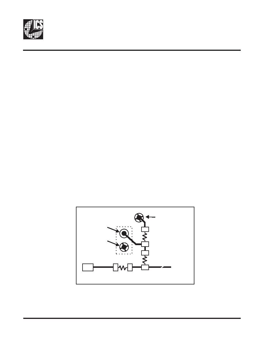
Via to
VDD
Clock trace to load
Series Term. Res.
Programming
Header
Via to Gnd
Device
Pad
2K
W
8.2K
W
Figure 1 shows a means of implementing this function
when a switch or 2 pin header is used. With no jumper is
installed the pin will be pulled high. With the jumper in
place the pin will be pulled low. If programmability is not
necessary, than only a single resistor is necessary. The
programming resistors should be located close to the
series termination resistor to minimize the current loop
area. It is more important to locate the series termination
resistor close to the driver than the programming resistor.
18
ICS951412
0883G--12/08/04
Ordering Information
ICS951412yFLFT
Example:
INDEX
AREA
INDEX
AREA
1 2
1 2
N
D
h x 45°
h x 45°
E1
E
SEATING
PLANE
SEATING
PLANE
A1
A
e
- C -
- C -
b
.10 (.004) C
.10 (.004) C
c
L
MIN
MAX
MIN
MAX
A
2.41
2.80
.095
.110
A1
0.20
0.40
.008
.016
b
0.20
0.34
.008
.0135
c
0.13
0.25
.005
.010
D
E
10.03
10.68
.395
.420
E1
7.40
7.60
.291
.299
e
h
0.38
0.64
.015
.025
L
0.50
1.02
.020
.040
N
a
0°
8°
0°
8°
VARIATIONS
MIN
MAX
MIN
MAX
56
18.31
18.55
.720
.730
10-0034
0.635 BASIC
0.025 BASIC
COMMON DIMENSIONS
In Millimeters
In Inches
COMMON DIMENSIONS
Reference Doc.: JEDEC Publication 95, MO-118
56-Lead, 300 mil Body, 25 mil, SSOP
N
SEE VARIATIONS
SEE VARIATIONS
D mm.
D (inch)
SYMBOL
SEE VARIATIONS
SEE VARIATIONS
Designation for tape and reel packaging
Lead Free (if required)
Package Type
F = SSOP
Revision Designator (will not correlate with datasheet revision)
Device Type (consists of 3 or 4 digit numbers)
Prefix
ICS, AV = Standard Device
ICS XXXX y F - LF T
19
ICS951412
0883G--12/08/04
Ordering Information
ICS951412yGLFT
Example:
INDEX
AREA
INDEX
AREA
1 2
1 2
N
D
E1
E
a
SEATING
PLANE
SEATING
PLANE
A1
A
A2
A2
e
- C -
- C -
b
c
L
aaa
C
MIN
MAX
MIN
MAX
A
--
1.20
--
.047
A1
0.05
0.15
.002
.006
A2
0.80
1.05
.032
.041
b
0.17
0.27
.007
.011
c
0.09
0.20
.0035
.008
D
E
E1
6.00
6.20
.236
.244
e
L
0.45
0.75
.018
.030
N
a
0°
8°
0°
8°
aaa
--
0.10
--
.004
VARIATIONS
MIN
MAX
MIN
MAX
56
13.90
14.10
.547
.555
10-0039
56-Lead 6.10 mm. Body, 0.50 mm. Pitch TSSOP
(240 mil) (20 mil)
SYMBOL
In Millimeters
In Inches
COMMON DIMENSIONS COMMON DIMENSIONS
SEE VARIATIONS
SEE VARIATIONS
8.10 BASIC
0.319 BASIC
0.50 BASIC
0.020 BASIC
SEE VARIATIONS
SEE VARIATIONS
N
D mm.
D (inch)
Reference Doc.: JEDEC Publication 95, MO-153
Designation for tape and reel packaging
Lead Free (if required)
Package Type
G = TSSOP
Revision Designator (will not correlate with datasheet revision)
Device Type (consists of 3 or 4 digit numbers)
Prefix
ICS, AV = Standard Device
ICS XXXX y G - LF T