 | –≠–ª–µ–∫—Ç—Ä–æ–Ω–Ω—ã–π –∫–æ–º–ø–æ–Ω–µ–Ω—Ç: ICS952621 | –°–∫–∞—á–∞—Ç—å:  PDF PDF  ZIP ZIP |

Integrated
Circuit
Systems, Inc.
ICS952621
0756A--09/10/04
Pin Configuration
Recommended Application:
CK409 48-pin part
Output Features:
∑
2 - 0.7V current-mode differential CPU pairs
∑
1 - 0.7V current-mode differential CPU pairs for ITP
∑
1 - 0.7V current-mode differential SRC pair
∑
9 - PCI (33MHz), including 3 free running PCI
∑
1 - USB, 48MHz
∑
1 - DOT, 48MHz
∑
2 - REF, 14.318MHz
∑
3 - 3V66, 66.66MHz
∑
1 - 3V66/VCH, selectable 48MHz or 66MHz
Key Specifications:
∑
CPU/SRC outputs cycle-cycle jitter < 125ps
∑
3V66 outputs cycle-cycle jitter < 250ps
∑
PCI outputs cycle-cycle jitter < 250ps
∑
CPU outputs skew: < 100ps
∑
+/- 300ppm frequency accuracy on CPU & SRC clocks
Programmable Timing Control HubTM for Next Gen P
4
TM processor
Functionality
Features/Benefits:
∑
Supports tight ppm accuracy clocks for Serial-ATA
∑
Supports spread spectrum modulation, 0 to -0.5%
down spread and +/- 0.25% center spread
∑
Supports CPU clks up to 400MHz in test mode
∑
Uses external 14.318MHz crystal
∑
Supports undriven differential CPU, SRC pair in PD#
and CPU_STOP# for power management.
48-pin SSOP
FS2
B6b5 FS_A FS_B
CPU
MHz
SRC
MHz
3V66
MHz
PCI
MHz
REF
MHz
USB/
DOT
MHz
0
0
100.00 100/200 66.66 33.33 14.318 48.00
0
1
200.00 100/200 66.66 33.33 14.318 48.00
1
0
133.33 100/200 66.66 33.33 14.318 48.00
1
1
166.66 100/200 66.66 33.33 14.318 48.00
0
0
200.00 100/200 66.66 33.33 14.318 48.00
0
1
400.00 100/200 66.66 33.33 14.318 48.00
1
0
266.66 100/200 66.66 33.33 14.318 48.00
1
1
333.33 100/200 66.66 33.33 14.318 48.00
0
1
FS_A/REF1
1
48 VDDA
FS_B/REF0
2
47 GND
VDDREF
3
46 IREF
X1
4
45 CPUCLKT_ITP
X2
5
44 CPUCLKC_ITP
GND
6
43 GND
PCICLK_F0
7
42 CPUCLKT1
PCICLK_F1
8
41 CPUCLKC1
PCICLK_F2
9
40 VDDCPU
VDDPCI 10
39 CPUCLKT0
GND 11
38 CPUCLKC0
PCICLK0 12
37 GND
PCICLK1 13
36 SRCCLKT
PCICLK2 14
35 SRCCLKC
PCICLK3 15
34 VDD
VDDPCI 16
33 VttPWR_GD#
GND 17
32 SDATA
PCICLK4 18
31 SCLK
PCICLK5 19
30 3V66_0
PD# 20
29 3V66_1
48MHz_DOT 21
28 GND
48MHz_USB 22
27 VDD3V66
GND 23
26 3V66_2
VDD48 24
25 3V66_3/VCH
ICS952621
**120K
pull-down
2
Integrated
Circuit
Systems, Inc.
ICS952621
0756A--09/10/04
Pin Description
PIN
#
PIN NAME
PIN TYPE
DESCRIPTION
1
FS_A/REF1
I/O
FS_A latched input for frequency select
Reference output, 14.318Hz
2
FS_B/REF0
I/O
FS_B latched input for frequency select
Reference output, 14.318Hz
3
VDDREF
PWR
Ref, XTAL power supply, nominal 3.3V
4
X1
IN
Crystal input, Nominally 14.318MHz.
5
X2
OUT
Crystal output, Nominally 14.318MHz
6
GND
PWR
Ground pin.
7
PCICLK_F0
OUT
Free running PCI clock not affected by PCI_STOP# .
8
PCICLK_F1
OUT
Free running PCI clock not affected by PCI_STOP# .
9
PCICLK_F2
OUT
Free running PCI clock not affected by PCI_STOP# .
10
VDDPCI
PWR
Power supply for PCI clocks, nominal 3.3V
11
GND
PWR
Ground pin.
12
PCICLK0
OUT
PCI clock output.
13
PCICLK1
OUT
PCI clock output.
14
PCICLK2
OUT
PCI clock output.
15
PCICLK3
OUT
PCI clock output.
16
VDDPCI
PWR
Power supply for PCI clocks, nominal 3.3V
17
GND
PWR
Ground pin.
18
PCICLK4
OUT
PCI clock output.
19
PCICLK5
OUT
PCI clock output.
20
PD#
IN
Asynchronous active low input pin, with 120Kohm internal pull-up resistor, used
to power down the device. The internal clocks are disabled and the VCO and
the crystal are stopped.
21
48MHz_DOT
OUT
48.008MHz Dot clock output
22
48MHz_USB
OUT
48.008MHz USB clock output
23
GND
PWR
Ground pin.
24
VDD48
PWR
Power for 48MHz output buffers and fixed PLL core.
25
3V66_3/VCH
OUT
3.3V 66.66MHz clock output
VCH: 48MHz VCH clock output
26
3V66_2
OUT
3.3V 66.66MHz clock output
27
VDD3V66
PWR
Power pin for the 3V66 clocks.
28
GND
PWR
Ground pin.
29
3V66_1
OUT
3.3V 66.66MHz clock output
30
3V66_0
OUT
3.3V 66.66MHz clock output
31
SCLK
IN
Clock pin of SMBus circuitry, 5V tolerant.
32
SDATA
I/O
Data pin for SMBus circuitry, 5V tolerant.
33
VttPWR_GD#
IN
This 3.3V LVTTL input is a level sensitive strobe used to determine when latch
inputs are valid and are ready to be sampled. This is an active low input.
34
VDD
OUT
Power supply, nominal 3.3V
35
SRCCLKC
OUT
Complementary clock of differential pair for S-ATA support.
+/- 300ppm accuracy required.
36
SRCCLKT
OUT
True clock of differential pair for S-ATA support.
+/- 300ppm accuracy required.
37
GND
PWR
Ground pin.
38
CPUCLKC0
OUT
Complementary clock of differential pair CPU outputs. These are current mode
outputs. External resistors are required for voltage bias.
39
CPUCLKT0
OUT
True clock of differential pair CPU outputs. These are current mode outputs.
External resistors are required for voltage bias.
40
VDDCPU
PWR
Supply for CPU clocks, 3.3V nominal
41
CPUCLKC1
OUT
Complementary clock of differential pair CPU outputs. These are current mode
outputs. External resistors are required for voltage bias.
42
CPUCLKT1
OUT
True clock of differential pair CPU outputs. These are current mode outputs.
External resistors are required for voltage bias.
43
GND
PWR
Ground pin.
44
CPUCLKC_ITP
OUT
"Complementary" clocks of differential pair CPU outputs for ITP.. These are
current mode outputs. External resistors are required for voltage bias.
45
CPUCLKT_ITP
OUT
"True" clocks of differential pair CPU outputs for ITP. These are current mode
outputs. External resistors are required for voltage bias.
46
IREF
OUT
This pin establishes the reference current for the differential current-mode
output pairs. This pin requires a fixed precision resistor tied to ground in order
to establish the appropriate current. 475 ohms is the standard value.
47
GND
PWR
Ground pin.
48
VDDA
PWR
3.3V power for the PLL core.
3
Integrated
Circuit
Systems, Inc.
ICS952621
0756A--09/10/04
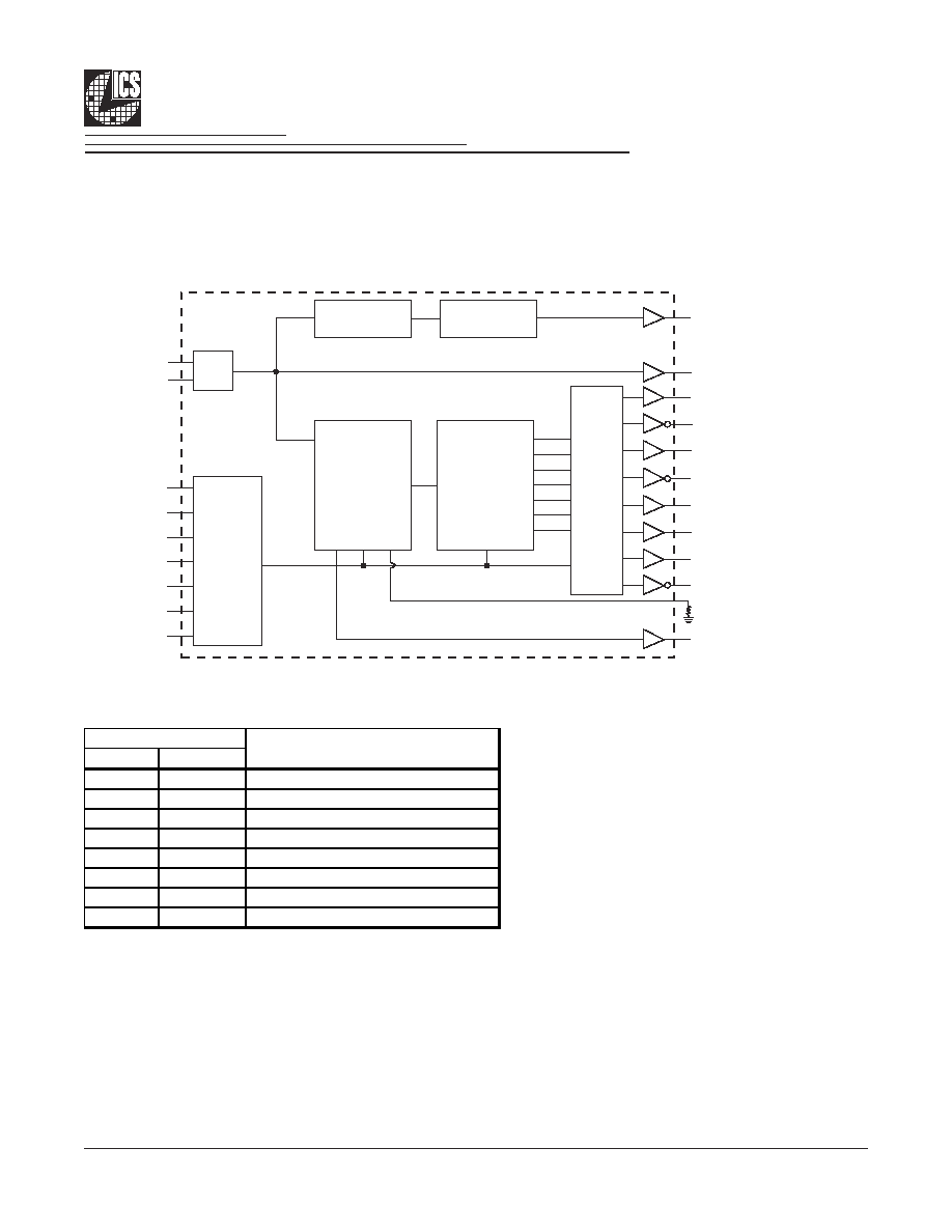
ICS962621 is a programmable 48 pin clock chip following Intel CK409 Yellow Cover specification. This clock synthesizer provides a single
chip solution for next generation P4 Intel processors and Intel chipsets. ICS962621 is driven with a 14.318MHz crystal. It generates CPU
outputs up to 200MHz. It also provides a tight ppm accuracy output for Serial ATA support.
General Description
Block Diagram
Power Groups
VDD
GND
3
6
Xtal, Ref
27
28
3V66 [0:3]
10,16
11,17
PCICLK outputs
34
37
SRCCLK outputs
48
47
Master clock, CPU Analog
24
23
48MHz, Fix Digital, Fix Analog
--
47
IREF
40
43
CPUCLK clocks
Description
Pin Number
I REF
PLL2
Frequency
Dividers
Programmable
Spread
PLL1
Programmable
Frequency
Dividers
STOP
Logic
48MHz, USB, DOT, VCH
X1
X2
XTAL
SDATA
SCLK
VTTPWRGD#
PD#
FS_A
FS_B
MODE
Control
Logic
REF (1:0)
CPUCLKT (1:0)
CPUCLKC (1:0)
SRCCLKT0
SRCCLKC0
3V66(3:0)
PCICLK (5:0), PCICLK_F (2:0)
CPUCLKT_ITP
RESET#
CPUCLKC_ITP
4
Integrated
Circuit
Systems, Inc.
ICS952621
0756A--09/10/04
Absolute Max
Symbol
Parameter
Min
Max
Units
VDD_A
3.3V Core Supply Voltage
V
DD +
0.5V
V
VDD_In
3.3V Logic Input Supply Voltage
-0.5
V
DD +
0.5V
V
Ts
Storage Temperature
-65
150
∞C
Tambient Ambient
Operating Temp
0
70
∞C
Tcase Case
Temperature
115
∞C
ESD prot
Input ESD protection
human body model
2000
V
Electrical Characteristics - Input/Supply/Common Output Parameters
T
A
= 0 - 70∞C; Supply Voltage V
DD
= 3.3 V +/-5%
PARAMETER
SYMBOL
CONDITIONS
MIN
TYP
MAX
UNITS NOTES
Input High Voltage
V
IH
3.3V +/-5%
2
V
DD
+ 0.3
V
Input Low Voltage
V
IL
3.3V +/-5%
V
SS
-
0.3
0.8
V
Input High Current
I
IH
V
IN
= V
DD
-5
5
uA
I
IL1
V
IN
= 0 V; Inputs with no pull-up
resistors
-5
uA
I
IL2
V
IN
= 0 V; Inputs with pull-up
resistors
-200
uA
Operating Supply Current
I
DD3.3OP
Full Active, C
L
= Full load;
260
350
mA
all diff pairs driven
0.3
35
mA
all differential pairs tri-stated
12
mA
Input Frequency
3
F
i
V
DD
= 3.3 V
14.31818
MHz
3
Pin Inductance
1
L
pin
7
nH
1
C
IN
Logic Inputs
5
pF
1
C
OUT
Output pin capacitance
6
pF
1
C
INX
X1 & X2 pins
5
pF
1
Clk Stabilization
1,2
T
STAB
From VDD Power-Up or de-
assertion of PD# to 1st clock.
1.8
ms
1,2
Modulation Frequency
Triangular Modulation
30
33
kHz
1
Tdrive_PD#
CPU output enable after
PD# de-assertion
300
us
1
Tfall_Pd#
PD# fall time of
5
ns
1
Trise_Pd#
PD# rise time of
5
ns
2
1
Guaranteed by design, not 100% tested in production.
2
See timing diagrams for timing requirements.
I
DD3.3PD
3
Input frequency should be measured at the REF output pin and tuned to ideal 14.31818MHz to meet
ppm frequency accuracy on PLL outputs.
Input Capacitance
1
Input Low Current
Powerdown Current
5
Integrated
Circuit
Systems, Inc.
ICS952621
0756A--09/10/04
Electrical Characteristics - CPU & SRC 0.7V Current Mode Differential Pair
T
A
= 0 - 70∞C; V
DD
= 3.3V +/-5%; C
L
=2pF
PARAMETER
SYMBOL
CONDITIONS
MIN
TYP
MAX
UNITS
NOTES
Current Source Output
Impedance
Zo
1
V
O
= V
x
3000
1
Voltage High
VHigh
660
749
850
1
Voltage Low
VLow
-150
3
150
1
Max Voltage
Vovs
756
1150
1
Min Voltage
Vuds
-300
-7
1
Crossing Voltage (abs) Vcross(abs)
250
350
550
mV
1
Crossing Voltage (var)
d-Vcross
Variation of crossing over all
edges
12
140
mV
1
Long Accuracy
ppm
see Tperiod min-max values
-300
0
300
ppm
1,2
200MHz nominal
4.9985
5.0000
5.0015
ns
2
200MHz spread
4.9985
5.0266
ns
2
166.66MHz nominal
5.9982
6.0000
6.0018
ns
2
166.66MHz spread
5.9982
6.0320
ns
2
133.33MHz nominal
7.4978
7.5000
7.5023
ns
2
133.33MHz spread
7.4978
5.4000
ns
2
100.00MHz nominal
9.9970 10.0000 10.0030
ns
2
100.00MHz spread
9.9970
10.0533
ns
2
200MHz nominal
4.8735
ns
1,2
166.66MHz nominal/spread
5.8732
ns
1,2
133.33MHz nominal/spread
7.3728
ns
1,2
100.00MHz nominal/spread
9.8720
ns
1,2
Rise Time
t
r
V
OL
= 0.175V, V
OH
= 0.525V
175
279
700
ps
1
Fall Time
t
f
V
OH
= 0.525V V
OL
= 0.175V
175
280
700
ps
1
Rise Time Variation
d-t
r
30
125
ps
1
Fall Time Variation
d-t
f
30
125
ps
1
Duty Cycle
d
t3
Measurement from differential
wavefrom
45
50.9
55
%
1
Skew
t
sk3
V
T
= 50%
8
100
ps
1
Jitter, Cycle to cycle
t
jcyc-cyc
Measurement from differential
wavefrom
40
125
ps
1
1
Guaranteed by design, not 100% tested in production.
SRC clock outputs run at only 100MHz or 200MHz, specs for 133.33 and 166.66 do not apply to SRC clock pair.
2
All Long Term Accuracy and Clock Period specifications are guaranteed with the assumption that Ref output is at
14.31818MHz
Tperiod
Average period
Absolute min period
T
absmin
Statistical measurement on single
ended signal using oscilloscope
math function.
mV
Measurement on single ended
signal using absolute value.
mV