 | ÐлекÑÑоннÑй компоненÑ: ICS954201 | СкаÑаÑÑ:  PDF PDF  ZIP ZIP |
Äîêóìåíòàöèÿ è îïèñàíèÿ www.docs.chipfind.ru
Integrated
Circuit
Systems, Inc.
ICS954201
0819G--12/06/04
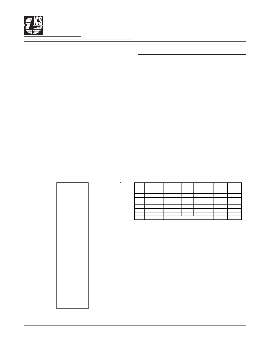
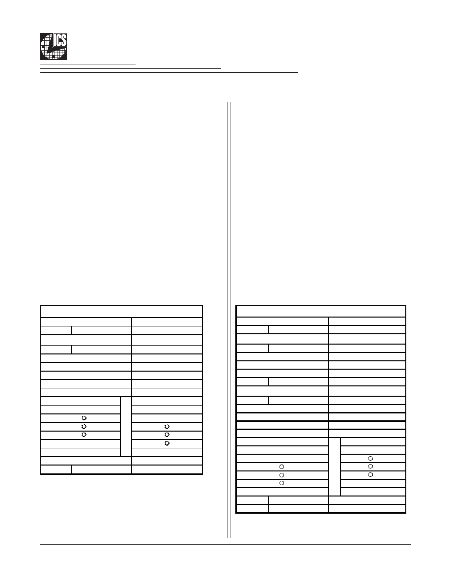
Pin Configuration
Recommended Application:
CK410M clock, Intel Yellow Cover part
Output Features:
·
2 - 0.7V current-mode differential CPU pairs
·
7 - 0.7V current-mode differential SRC pair for SATA and
PCI-E
·
1 - 0.7V current-mode differential CPU/SRC selectable
pair
·
4 - PCI (33MHz)
·
2 - PCICLK_F, (33MHz) free-running
·
1 - USB, 48MHz
·
1 - DOT, 96MHz, 0.7V current differential pair
·
1 - REF, 14.318MHz
Key Specifications:
·
CPU outputs cycle-cycle jitter < 85ps
·
SRC outputs cycle-cycle jitter < 125ps
·
PCI outputs cycle-cycle jitter < 500ps
·
+/- 300ppm frequency accuracy on CPU & SRC clocks
·
+/- 100ppm frequency accuracy on USB clocks
Programmable Timing Control HubTM for Mobile P
4
TM Systems
Functionality
Features/Benefits:
·
Supports tight ppm accuracy clocks for Serial-ATA and
PCI-Express
·
Supports spread spectrum modulation, 0 to -0.5%
down spread
·
Supports CPU clocks up to 400MHz
·
Uses external 14.318MHz crystal, external crystal load
caps are required for frequency tuning
·
Supports undriven differential CPU, SRC pair in PD#
for power management.
56-pin SSOP & TSSOP
VDDPCI 1
56 PCICLK2
GND 2
55 PCI/SRC_STOP#
PCICLK3 3
54 CPU_STOP#
PCICLK4 4
53 FS_C/TEST_SEL
PCICLK5 5
52 REFOUT
GND 6
51 GND
VDDPCI 7
50 X1
ITP_EN/PCICLK_F0 8
49 X2
PCICLK_F1 9
48 VDDREF
Vtt_PwrGd#/PD 10
47 SDATA
VDD48 11
46 SCLK
USB_48MHz/FS_A 12
45 GND
GND 13
44 CPUCLKT0
DOTT_96MHz 14
43 CPUCLKC0
DOTC_96MHz 15
42 VDDCPU
FS_B/TEST_MODE 16
41 CPUCLKT1
SRCCLKT0 17
40 CPUCLKC1
SRCCLKC0 18
39 IREF
SRCCLKT1 19
38 GNDA
SRCCLKC1 20
37 VDDA
VDDSRC 21
36 CPUCLKT2_ITP/SRCCLKT7
SRCCLKT2 22
35 CPUCLKC2_ITP/SRCCLKC7
SRCCLKC2 23
34 VDDSRC
SRCCLKT3 24
33 SRCCLKT6
SRCCLKC3 25
32 SRCCLKC6
SRCCLKT4_SATA 26
31 SRCCLKT5
SRCCLKC4_SATA 27
30 SRCCLKC5
VDDSRC 28
29 GND
I
C
S
954201
FS_C
1
FS_B
2
FS_A
2
CPU
MHz
SRC
MHz
PCI
MHz
REF
MHz
U
SB
MHz
DOT
MHz
0
0
0
266.66
100.00
33.33 14.318
48.00
96.00
0
0
1
133.33
100.00
33.33 14.318
48.00
96.00
0
1
0
200.00
100.00
33.33 14.318
48.00
96.00
0
1
1
166.66
100.00
33.33 14.318
48.00
96.00
1
0
0
333.33
100.00
33.33 14.318
48.00
96.00
1
0
1
100.00
100.00
33.33 14.318
48.00
96.00
1
1
0
400.00
100.00
33.33 14.318
48.00
96.00
1
1
1
14.318
48.00
96.00
1. FS_C is a three-level input. Please see V
IL_FS
and V
IH_FS
specifications in
the Input/Supply/Common Output Parameters Table for correct values.
Also refer to the Test Clarification Table.
2. FS_B and FS_A are low-threshold inputs. Please see the V
IL_FS
and V
IH_FS
specifications in the Input/Supply/Common Output Parameters Table for correct values.
RESERVED
2
Integrated
Circuit
Systems, Inc.
ICS954201
0819G--12/06/04
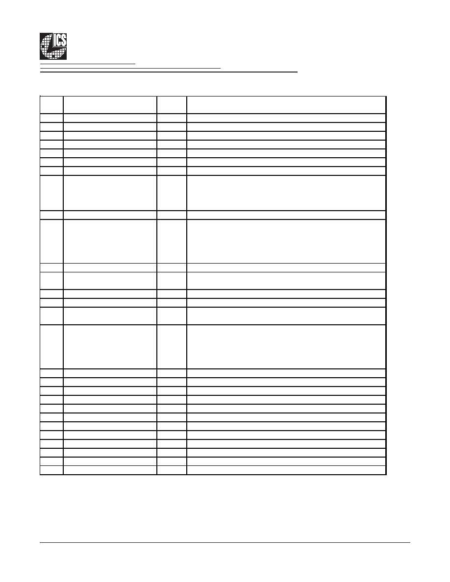
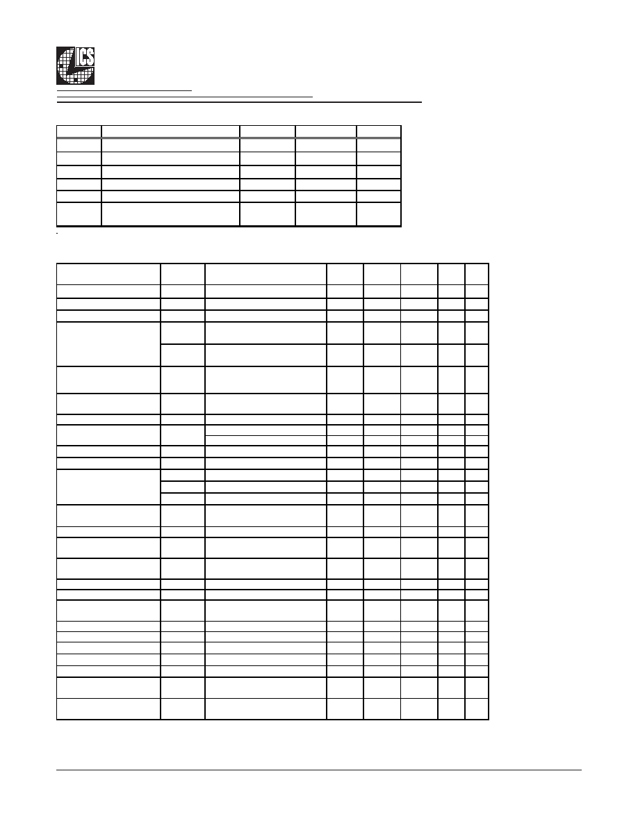
Pin Description
PIN # PIN NAME
PIN
TYPE
DESCRIPTION
1
VDDPCI
PWR
Power supply for PCI clocks, nominal 3.3V
2
GND
PWR
Ground pin.
3
PCICLK3
OUT
PCI clock output.
4
PCICLK4
OUT
PCI clock output.
5
PCICLK5
OUT
PCI clock output.
6
GND
PWR
Ground pin.
7
VDDPCI
PWR
Power supply for PCI clocks, nominal 3.3V
8
ITP_EN/PCICLK_F0
I/O
Free running PCI clock not affected by PCI_STOP#.
ITP_EN: latched input to select pin functionality
1 = CPU_ITP pair
0 = SRC pair
9
PCICLK_F1
OUT
Free running PCI clock not affected by PCI_STOP# .
10
Vtt_PwrGd#/PD
IN
Vtt_PwrGd# is an active low input used to determine when
latched inputs are ready to be sampled. PD is an asynchronous
active high input pin used to put the device into a low power
state. The internal clocks, PLLs and the crystal oscillator are
stopped.
11
VDD48
PWR
Power pin for the 48MHz output.3.3V
12
USB_48MHz/FS_A
I/O
Frequency select latch input pin / Fixed 48MHz USB clock
output. 3.3V.
13
GND
PWR
Ground pin.
14
DOTT_96MHz
OUT
True clock of differential pair for 96.00MHz DOT clock.
15
DOTC_96MHz
OUT
Complement clock of differential pair for 96.00MHz DOT clock.
16
FS_B/TEST_MODE
IN
3.3V tolerant input for CPU frequency selection. Refer to input
electrical characteristics for Vil_FS and Vih_FS values.
TEST_MODE is a real time input to select between Hi-Z and
REF/N divider mode while in test mode. Refer to Test
Clarification Table.
17
SRCCLKT0
OUT
True clock of differential SRC clock pair.
18
SRCCLKC0
OUT
Complement clock of differential SRC clock pair.
19
SRCCLKT1
OUT
True clock of differential SRC clock pair.
20
SRCCLKC1
OUT
Complement clock of differential SRC clock pair.
21
VDDSRC
PWR
Supply for SRC clocks, 3.3V nominal
22
SRCCLKT2
OUT
True clock of differential SRC clock pair.
23
SRCCLKC2
OUT
Complement clock of differential SRC clock pair.
24
SRCCLKT3
OUT
True clock of differential SRC clock pair.
25
SRCCLKC3
OUT
Complement clock of differential SRC clock pair.
26
SRCCLKT4_SATA
OUT
True clock of differential SRC/SATA pair.
27
SRCCLKC4_SATA
OUT
Complement clock of differential SRC/SATA pair.
28
VDDSRC
PWR
Supply for SRC clocks, 3.3V nominal
3
Integrated
Circuit
Systems, Inc.
ICS954201
0819G--12/06/04
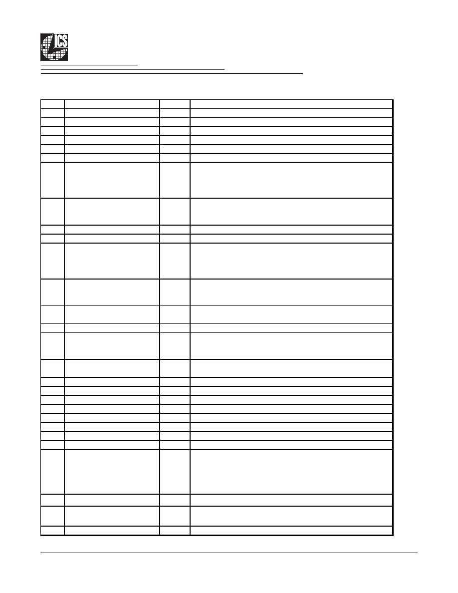
Pin Description (Continued)
PIN # PIN NAME
TYPE
DESCRIPTION
29
GND
PWR
Ground pin.
30
SRCCLKC5
OUT
Complement clock of differential SRC clock pair.
31
SRCCLKT5
OUT
True clock of differential SRC clock pair.
32
SRCCLKC6
OUT
Complement clock of differential SRC clock pair.
33
SRCCLKT6
OUT
True clock of differential SRC clock pair.
34
VDDSRC
PWR
Supply for SRC clocks, 3.3V nominal
35
CPUCLKC2_ITP/SRCCLKC7
OUT
Complimentary clock of CPU_ITP/SRC differential pair
CPU_ITP/SRC output. These are current mode outputs.
External resistors are required for voltage bias. Selected by
ITP_EN input.
36
CPUCLKT2_ITP/SRCCLKT7
OUT
True clock of CPU_ITP/SRC differential pair CPU_ITP/SRC
output. These are current mode outputs. External resistors are
required for voltage bias. Selected by ITP_EN input.
37
VDDA
PWR
3.3V power for the PLL core.
38
GNDA
PWR
Ground pin for the PLL core.
39
IREF
OUT
This pin establishes the reference current for the differential
current-mode output pairs. This pin requires a fixed precision
resistor tied to ground in order to establish the appropriate
current. 475 ohms is the standard value.
40
CPUCLKC1
OUT
Complimentary clock of differential pair CPU outputs. These are
current mode outputs. External resistors are required for voltage
bias.
41
CPUCLKT1
OUT
True clock of differential pair CPU outputs. These are current
mode outputs. External resistors are required for voltage bias.
42
VDDCPU
PWR
Supply for CPU clocks, 3.3V nominal
43
CPUCLKC0
OUT
Complimentary clock of differential pair CPU outputs. These are
current mode outputs. External resistors are required for voltage
bias.
44
CPUCLKT0
OUT
True clock of differential pair CPU outputs. These are current
mode outputs. External resistors are required for voltage bias.
45
GND
PWR
Ground pin.
46
SCLK
IN
Clock pin of SMBus circuitry, 5V tolerant.
47
SDATA
I/O
Data pin for SMBus circuitry, 5V tolerant.
48
VDDREF
PWR
Ref, XTAL power supply, nominal 3.3V
49
X2
OUT
Crystal output, Nominally 14.318MHz
50
X1
IN
Crystal input, Nominally 14.318MHz.
51
GND
PWR
Ground pin.
52
REFOUT
OUT
Reference Clock output
53
FS_C/TEST_SEL
IN
3.3V tolerant input for CPU frequency selection. Low voltage
threshold inputs, see input electrical characteristics for Vil_FS
and Vih_FS values.
TEST_Sel: 3-level latched input to enable test mode.
Refer to Test Clarification Table
54
CPU_STOP#
IN
Stops all CPUCLK, except those set to be free running clocks
55
PCI/SRC_STOP#
IN
Stops all PCICLKs and SRCCLKs besides the free-running
clocks at logic 0 level, when input low
56
PCICLK2
OUT
PCI clock output.
4
Integrated
Circuit
Systems, Inc.
ICS954201
0819G--12/06/04
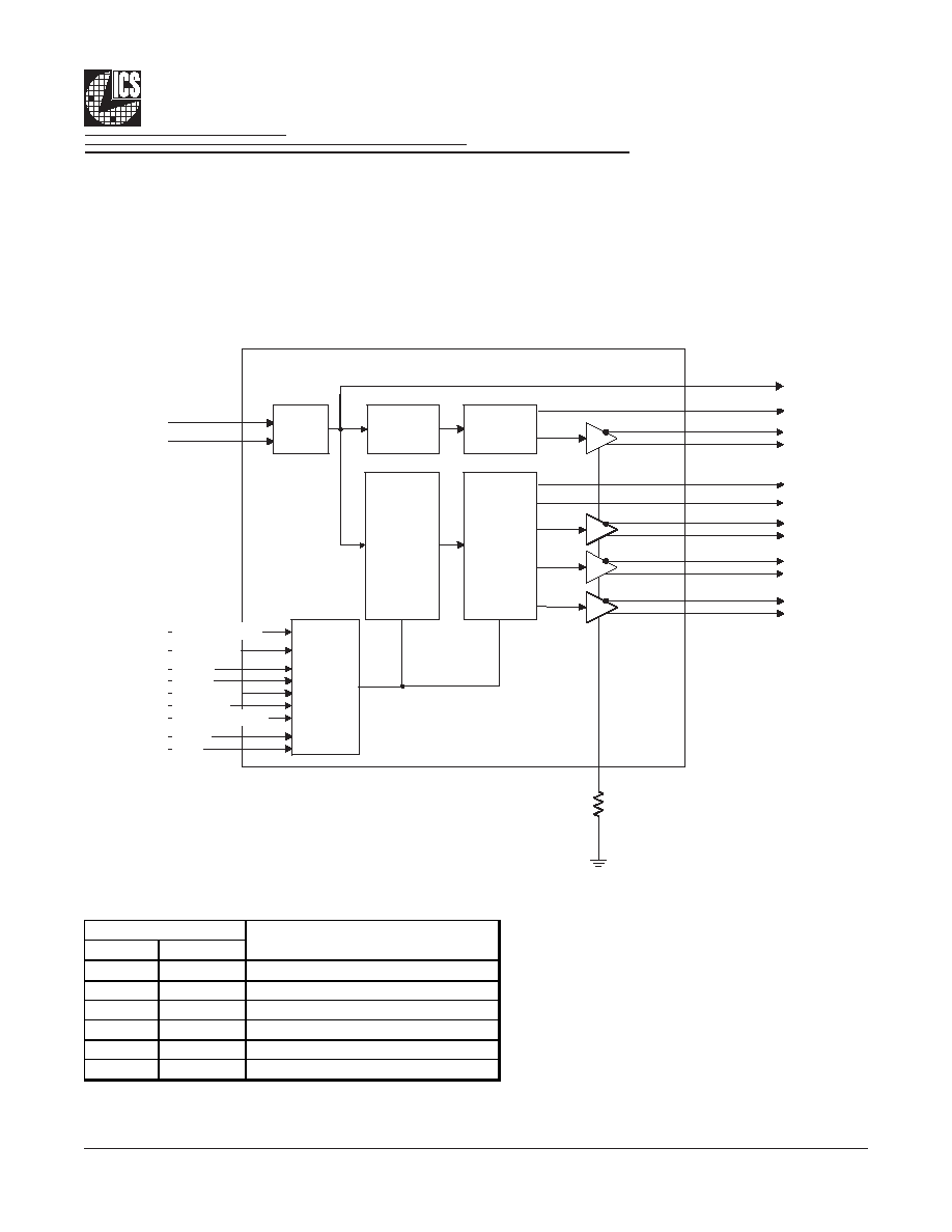
ICS954201 is a CK410M Yellow Cover clock synthesizer. ICS954201 provides a single-chip solution for mobile systems built
with Intel P4-M processors and Intel mobile chipsets. ICS954201 is driven with a 14.318MHz crystal and generates CPU
outputs up to 400MHz. It provides the tight ppm accuracy required by Serial ATA and PCI-Express.
General Description
Block Diagram
Power Groups
VDD
GND
48
51
Xtal, Ref
1,7
2,6
PCICLK outputs
21,28,34
29
SRCCLK outputs
37
38
Master clock, CPU Analog
11
13
DOT, USB, PLL_48
42
45
CPUCLK clocks
Description
Pin Number
PROG.
SPREAD
MAIN PLL
PCICLK(5:2)
CONTROL
LOGIC
XTAL
OSC.
CPUCLK(1:0)
FIXED PLL
USB_48MHz
DIVIDER
PROG.
DIVIDERS
REF
SRCCLK(6:0)
ITP_EN
SDATA
SCLK
TEST_MODE
X1
X2
IREF
FS(C:A)
TEST_SEL
VTT_PWRGD#/PD
DOT_96MHz
PCICLK_F(1:0)
CPUCLK2_ITP/SRCCLK7
PCI/SRC_STOP#
CPU_STOP#
5
Integrated
Circuit
Systems, Inc.
ICS954201
0819G--12/06/04
General I
2
C serial interface information for the ICS954201
How to Write:
· Controller (host) sends a start bit.
· Controller (host) sends the write address D2
(H)
· ICS clock will
acknowledge
· Controller (host) sends the begining byte location = N
· ICS clock will
acknowledge
· Controller (host) sends the data byte count = X
· ICS clock will
acknowledge
· Controller (host) starts sending
Byte N through
Byte N + X -1
(see Note 2)
· ICS clock will
acknowledge each byte one at a time
· Controller (host) sends a Stop bit
How to Read:
· Controller (host) will send start bit.
· Controller (host) sends the write address D2
(H)
· ICS clock will
acknowledge
· Controller (host) sends the begining byte
location = N
· ICS clock will
acknowledge
· Controller (host) will send a separate start bit.
· Controller (host) sends the read address D3
(H)
· ICS clock will
acknowledge
· ICS clock will send the data byte count = X
· ICS clock sends
Byte N + X -1
· ICS clock sends
Byte 0 through byte X (if X
(H)
was written to byte 8)
.
· Controller (host) will need to acknowledge each byte
· Controllor (host) will send a not acknowledge bit
· Controller (host) will send a stop bit
ICS (Slave/Receiver)
T
WR
ACK
ACK
ACK
ACK
ACK
P
stoP bit
X By
t
e
Index Block Write Operation
Slave Address D2
(H)
Beginning Byte = N
WRite
starT bit
Controller (Host)
Byte N + X - 1
Data Byte Count = X
Beginning Byte N
T
starT bit
WR
WRite
RT
Repeat starT
RD
ReaD
Beginning Byte N
Byte N + X - 1
N
Not acknowledge
P
stoP bit
Slave Address D3
(H)
Index Block Read Operation
Slave Address D2
(H)
Beginning Byte = N
ACK
ACK
Data Byte Count = X
ACK
ICS (Slave/Receiver)
Controller (Host)
X Byt
e
ACK
ACK
6
Integrated
Circuit
Systems, Inc.
ICS954201
0819G--12/06/04
Absolute Max
Symbol
Parameter
Min
Max
Units
VDD_A
3.3V Core Supply Voltage
V
DD
+ 0.5V
V
VDD_In
3.3V Logic Input Supply Voltage
GND - 0.5
V
DD
+ 0.5V
V
Ts
Storage Temperature
-65
150
°
C
Tambient Ambient
Operating
Temp
0
70
°C
Tcase Case
Temperature
115
°C
ESD prot
Input ESD protection
human body model
2000
V
Electrical Characteristics - Input/Supply/Common Output Parameters
T
A
= 0 - 70°C; Supply Voltage V
DD
= 3.3 V +/-5%
PARAMETER
SYMBOL
CONDITIONS
MIN
TYP
MAX
UNITS Notes
Input High Voltage
V
IH
3.3 V +/-5%
2
V
DD
+ 0.3
V
1
Input Low Voltage
V
IL
3.3 V +/-5%
V
SS
- 0.3
0.8
V
1
Input High Current
I
IH
V
IN
= V
DD
-5
5
uA
1
I
IL1
V
IN
= 0 V; Inputs with no pull-up
resistors
-5
uA
1
I
IL2
V
IN
= 0 V; Inputs with pull-up
resistors
-200
uA
1
Low Threshold Input High
Voltage
V
IH_FS
3.3 V +/-5%
0.7
V
DD
+ 0.3
V
1
Low Threshold Input Low
Voltage
V
IL_FS
3.3 V +/-5%
V
SS
- 0.3
0.35
V
1
Operating Supply Current
I
DD3.3OP
Full Active, C
L
= Full load;
278
400
mA
all diff pairs driven
67
70
mA
all differential pairs tri-stated
4.8
12
mA
Input Frequency
3
F
i
V
DD
= 3.3 V
14.31818
MHz
3
Pin Inductance
1
L
pin
7
nH
1
C
IN
Logic Inputs
5
pF
1
C
OUT
Output pin capacitance
6
pF
1
C
INX
X1 & X2 pins
5
pF
1
Clk Stabilization
1,2
T
STAB
From V
DD
Power-Up or de-
assertion of PD# to 1st clock
1.3
1.8
ms
1,2
Modulation Frequency
Triangular Modulation
30
33
kHz
1
Tdrive_SRC
SRC output enable after
PCI_STOP de-assertion
8
10
ns
1
Tdrive_PD
Differential output enable after
PD# de-assertion
300
us
1
Tfall_PD
PD# fall time of
5
ns
1
Trise_PD
PD# rise time of
5
ns
2
Tdrive_CPU_STOP
CPU output enable after
CPU_STOP de-assertion
8
10
ns
1
Tfall_CPU_STOP
CPU_STOP fall time of
5
ns
1
Trise_CPU_STOP#
CPU_STOP rise time of
5
ns
2
SMBus Voltage
V
DD
2.7
5.5
V
1
Low-level Output Voltage
V
OL
SDATA, SCLK @ I
PULLUP
0.4
V
1
Current sinking
I
PULLUP
V
OL
= 0.4 V
4
mA
1
SCLK/SDATA
Clock/Data Rise Time
T
RI2C
(Max VIL - 0.15) to
(Min VIH + 0.15)
1000
ns
1,3
SCLK/SDATA
Clock/Data Fall Time
T
FI2C
(Min VIH + 0.15) to
(Max VIL - 0.15)
300
ns
1,3
1
Guaranteed by design, not 100% tested in production.
2
See timing diagrams for timing requirements.
3
Input frequency should be measured at the REF output pin and tuned to ideal 14.31818MHz to meet
Input Low Current
Powerdown Current
I
DD3.3PD
Input Capacitance
1
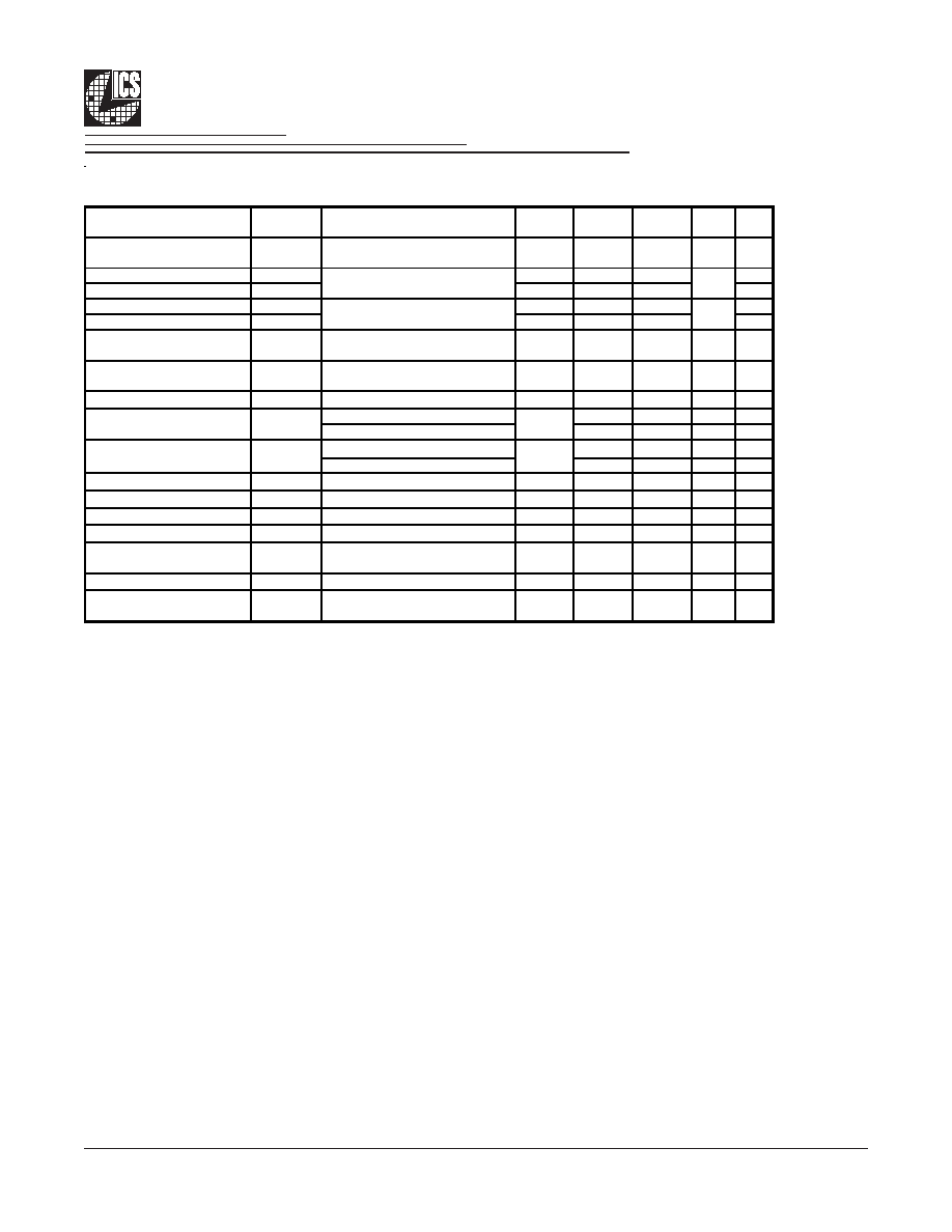
7
Integrated
Circuit
Systems, Inc.
ICS954201
0819G--12/06/04
Electrical Characteristics - SRC 0.7V Current Mode Differential Pair
T
A
= 0 - 70°C; V
DD
= 3.3 V +/-5%; C
L
=2pF, R
S
=33.2
, R
P
=49.9
,
REF
= 475
PARAMETER
SYMBOL
CONDITIONS
MIN
TYP
MAX
UNITS Notes
Current Source Output
Impedance
Zo
1
V
O
= V
x
3000
1
Voltage High
VHigh
660
760
850
1,3
Voltage Low
VLow
-150
2
150
1,3
Max Voltage
Vovs
782
1150
1
Min Voltage
Vuds
-300
-33
1
Crossing Voltage (abs)
Vcross
(abs)
250
344
550
mV
1
Crossing Voltage (var)
d-Vcross
Variation of crossing over all
edges
97
140
mV
1
Long Accuracy
ppm
see T
period
min-max values
-300
300
ppm
1,2
100.00MHz non-spread
9.9999
10.0030
ns
2
100.00MHz spread
10.0533
ns
2
100.00MHz non-spread
9.9999
10.1280
ns
1,2
100.00MHz spread
10.1783
ns
1,2
Rise Time
t
r
V
OL
= 0.175V, V
OH
= 0.525V
175
260
700
ps
1
Fall Time
t
f
V
OH
= 0.525V, V
OL
= 0.175V
175
212
700
ps
1
Rise Time Variation
d-t
r
20
125
ps
1
Fall Time Variation
d-t
f
13
125
ps
1
Duty Cycle
d
t3
Measurement from differential
wavefrom
45
51
55
%
1
Skew
t
sk3
V
T
= 50%
87
250
ps
1
Jitter, Cycle to cycle
t
jcyc-cyc
Measurement from differential
wavefrom
37
125
ps
1
1
Guaranteed by design and characterization, not 100% tested in production.
2
All Long Term Accuracy and Clock Period specifications are guaranteed assuming that REFOUT is at 14.31818MHz
3
I
REF
= V
DD
/(3xR
R
). For R
R
= 475
(1%), I
REF
= 2.32mA. I
OH
= 6 x I
REF
and V
OH
= 0.7V @ Z
O
=50
.
9.8720
Absolute min/max period
T
abs
mV
Measurement on single ended
signal using absolute value.
mV
Average period
T
period
Statistical measurement on single
ended signal using oscilloscope
9.9970
8
Integrated
Circuit
Systems, Inc.
ICS954201
0819G--12/06/04
Electrical Characteristics - CPU 0.7V Current Mode Differential Pair
T
A
= 0 - 70°C; V
DD
= 3.3 V +/-5%; C
L
=2pF, R
S
=33.2
, R
P
=49.9
,
REF
= 475
PARAMETER
SYMBOL
CONDITIONS
MIN
TYP
MAX
UNITS Notes
Current Source Output
Impedance
Zo
V
O
= V
x
3000
1
Voltage High
VHigh
660
727
850
1,3
Voltage Low
VLow
-150
-2
150
1,3
Max Voltage
Vovs
752
1150
1
Min Voltage
Vuds
-300
-21
1
Crossing Voltage (abs)
Vcross
(abs)
250
348
550
mV
1
Crossing Voltage (var)
d-Vcross
Variation of crossing over all
edges
39
140
mV
1
Long Accuracy
ppm
see Tperiod min-max values
-300
300
ppm
1,2
400MHz non-spread
2.4993
2.4999
2.5008
ns
2
400MHz spread
2.4993
2.5133
ns
2
333.33MHz non-spread
2.9991
3.0000
3.0009
ns
2
333.33MHz spread
2.9991
3.016
ns
2
266.66MHz non-spread
3.7489
3.7509
3.7511
ns
2
266.66MHz spread
3.7489
3.77
ns
2
200MHz non-spread
4.9985
4.9998
5.0015
ns
2
200MHz spread
4.9985
5.0266
ns
2
166.66MHz non-spread
5.9982
6.0000
6.0018
ns
2
166.66MHz spread
5.9982
6.0320
ns
2
133.33MHz non-spread
7.4978
7.5017
7.5023
ns
2
133.33MHz spread
7.4978
5.4000
ns
2
100.00MHz non-spread
9.9970
10.0000
10.0030
ns
2
100.00MHz spread
9.9970
10.0533
ns
2
400MHz non-spread
2.4970
2.5750
ns
1,2
400MHz spread
2.5983
ns
1,2
333.33MHz non-spread
2.9940
3.0859
ns
1,2
333.33MHz spread
3.1010
ns
1,2
266.66MHz non-spread
3.7430
3.8361
ns
1,2
266.66MHz spread
3.8550
ns
1,2
200MHz non-spread
4.9940
5.0865
ns
1,2
200MHz spread
5.1116
ns
1,2
166.66MHz non-spread
5.9950
6.0868
ns
1,2
166.66MHz spread
6.1170
ns
1,2
133.33MHz non-spread
7.4970
7.5873
ns
1,2
133.33MHz spread
7.6250
ns
1,2
100.00MHz non-spread
10.0000
10.0880
ns
1,2
100.00MHz spread
10.1383
ns
1,2
Rise Time
t
r
V
OL
= 0.175V, V
OH
= 0.525V
175
230
700
ps
1
Fall Time
t
f
V
OH
= 0.525V V
OL
= 0.175V
175
206
700
ps
1
Rise Time Variation
d-t
r
15
125
ps
1
Fall Time Variation
d-t
f
14
125
ps
1
Duty Cycle
d
t3
Measurement from differential
wavefrom
45
51
55
%
1
CPU(1:0), V
T
= 50%
7.5
100
ps
1
CPU2_ITP, V
T
= 50%
145
150
ps
1
Jitter, Cycle to cycle
t
jcyc-cyc
Differential waveform
measurement, CPU(1:0)
36
85
ps
1
Jitter, Cycle to cycle
t
jcyc-cyc
Differential waveform
measurement, CPU2_ITP
96
125
ps
1
1
Guaranteed by design and characterization, not 100% tested in production.
2
All Long Term Accuracy and Clock Period specifications are guaranteed assuming that REFOUT is at 14.31818MHz
3
I
REF
= V
DD
/(3xR
R
). For R
R
= 475
(1%), I
REF
= 2.32mA. I
OH
= 6 x I
REF
and V
OH
= 0.7V @ Z
O
=50
.
2.4143
2.9141
Average period
T
period
Absolute min/max period
T
abs
9.9120
Statistical measurement on single
ended signal using oscilloscope
math function.
mV
Measurement on single ended
signal using absolute value.
mV
Skew
t
sk3
3.6639
4.9135
5.9132
7.4128
9
Integrated
Circuit
Systems, Inc.
ICS954201
0819G--12/06/04
Electrical Characteristics - PCICLK/PCICLK_F
T
A
= 0 - 70°C; V
DD
= 3.3 V +/-5%; C
L
= 10-20 pF (unless otherwise specified)
PARAMETER
SYMBOL
CONDITIONS
MIN
TYP
MAX
UNITS Notes
Long Accuracy
ppm
see Tperiod min-max values
-300
35
300
ppm
1,2
33.33MHz output non-spread
29.9989
30.0090
ns
2
33.33MHz output spread
30.0752
30.1598
ns
2
33.33MHz output non-spread
30.5090
ns
1,2
33.33MHz output spread
30.6598
ns
1,2
Output High Voltage
V
OH
I
OH
= -1 mA
2.4
3.25
V
1
Output Low Voltage
V
OL
I
OL
= 1 mA
0.05
0.55
V
1
V
OH
@MIN = 1.0 V
-33
-62
mA
1
V
OH
@ MAX = 3.135 V
-10
-33
mA
1
V
OL
@ MIN = 1.95 V
30
61
mA
1
V
OL
@ MAX = 0.4 V
23
38
mA
1
Edge Rate
Rising edge rate
1
1.60
4
V/ns
1
Edge Rate
Falling edge rate
1
1.71
4
V/ns
1
Rise Time
t
r1
V
OL
= 0.4 V, V
OH
= 2.4 V
0.5
1.25
2
ns
1
Fall Time
t
f1
V
OH
= 2.4 V, V
OL
= 0.4 V
0.5
1.17
2
ns
1
Duty Cycle
d
t1
V
T
= 1.5 V
45
50
55
%
1
Skew t
sk1
V
T
= 1.5 V
81
500
ps
1
Jitter
t
jcyc-cyc
V
T
= 1.5 V
250
500
ps
1
1
Guaranteed by design and characterization, not 100% tested in production.
2
All Long Term Accuracy and Clock Period specifications are guaranteed assuming that REFOUT is at 14.31818MHz
Output Low Current
I
OL
Clock period
T
period
Output High Current
I
OH
29.9910
Absolute min/max period
T
abs
29.4910
Electrical Characteristics - 48MHz, USB
T
A
= 0 - 70°C; V
DD
= 3.3 V +/-5%; C
L
= 10-20 pF (unless otherwise specified)
PARAMETER
SYMBOL
CONDITIONS
MIN
TYP
MAX
UNITS Notes
Long Accuracy
ppm
see Tperiod min-max values
-100
0.25
100
ppm
1,2
Clock period
T
period
48.00000 MHz output
20.8313
20.8333
20.8354
ns
2
Absolute min/max period
T
abs
48.00000 MHz output
20.4813
21.1854
ns
1,2
Output High Voltage
V
OH
I
OH
= -1 mA
2.4
3.25
V
1
Output Low Voltage
V
OL
I
OL
= 1 mA
0.05
0.55
V
1
V
OH
@ MIN = 1.0 V
-29
-53
mA
1
V
OH
@ MAX = 3.135 V
-6.2
-23
mA
1
V
OL
@MIN = 1.95 V
29
61
mA
1
V
OL
@ MAX = 0.4 V
23
27
mA
1
Edge Rate
Rising edge rate
1
1.53
2
V/ns
1
Edge Rate
Falling edge rate
1
1.68
2
V/ns
1
Rise Time
t
r1
V
OL
= 0.4 V, V
OH
= 2.4 V
1
1.31
2
ns
1
Fall Time
t
f1
V
OH
= 2.4 V, V
OL
= 0.4 V
1
1.19
2
ns
1
Duty Cycle
d
t1
V
T
= 1.5 V
45
52
55
%
1
Jitter, Cycle to cycle
t
jcyc-cyc
V
T
= 1.5 V
139
350
ps
1
1
Guaranteed by design and characterization, not 100% tested in production.
2
All Long Term Accuracy and Clock Period specifications are guaranteed assuming that REFOUT is at 14.31818MHz
Output Low Current
I
OL
Output High Current
I
OH
10
Integrated
Circuit
Systems, Inc.
ICS954201
0819G--12/06/04
Electrical Characteristics - DOT, 96MHz 0.7V Current Mode Differential Pair
T
A
= 0 - 70°C; V
DD
= 3.3 V +/-5%; C
L
=2pF, R
S
=33.2
, R
P
=49.9
,
REF
= 475
PARAMETER
SYMBOL
CONDITIONS
MIN
TYP
MAX
UNITS Notes
Current Source Output
Impedance
Zo
1
V
O
= V
x
3000
1
Voltage High
VHigh
660
749
850
1,3
Voltage Low
VLow
-150
1.5
150
1,3
Max Voltage
Vovs
778
1150
1
Min Voltage
Vuds
-300
-51
1
Crossing Voltage (abs)
Vcross
(abs)
250
358
550
mV
1
Crossing Voltage (var)
d-Vcross
Variation of crossing over all
edges
26
140
mV
1
Long Accuracy
ppm
see T
period
min-max values
-100
100
ppm
1,2
Average period
T
period
96.00MHz
10.4156
10.4167
10.4177
ns
2
Absolute min/max period
T
abs
96.00MHz
10.1656
10.4100
10.6677
ns
1,2
Rise Time
t
r
V
OL
= 0.175V, V
OH
= 0.525V
175
210
700
ps
1
Fall Time
t
f
V
OH
= 0.525V, V
OL
= 0.175V
175
180
700
ps
1
Rise Time Variation
d-t
r
23
125
ps
1
Fall Time Variation
d-t
f
50
125
ps
1
Duty Cycle
d
t3
Measurement from differential
wavefrom
45
49
55
%
1
Jitter, Cycle to cycle
t
jcyc-cyc
Measurement from differential
wavefrom
98
250
ps
1
1
Guaranteed by design and characterization, not 100% tested in production.
2
All Long Term Accuracy and Clock Period specifications are guaranteed assuming that REFOUT is at 14.31818MHz
3
I
REF
= V
DD
/(3xR
R
). For R
R
= 475
(1%), I
REF
= 2.32mA. I
OH
= 6 x I
REF
and V
OH
= 0.7V @ Z
O
=50
.
Measurement on single ended
signal using absolute value.
mV
Statistical measurement on single
ended signal using oscilloscope
mV
Electrical Characteristics - REF-14.318MHz
T
A
= 0 - 70°C; V
DD
= 3.3 V +/-5%; C
L
= 10-20 pF (unless otherwise specified)
PARAMETER
SYMBO
L
CONDITIONS
MIN
TYP
MAX
UNITS Notes
Long Accuracy
ppm
see Tperiod min-max values
-300
300
ppm
1
Clock period
T
period
14.318MHz output nominal
69.8270
69.841
69.8550
ns
1
Output High Voltage
V
OH
I
OH
= -1 mA
2.4
3.25
V
1
Output Low Voltage
V
OL
I
OL
= 1 mA
0.05
0.4
V
1
V
OH
@ MIN = 1.0 V
-33
-53
mA
1
V
OH
@ MAX = 3.135 V
-6
-33
mA
1
V
OL
@MIN = 1.95 V
30
60.9
mA
1
V
OL
@ MAX = 0.4 V
23
38
mA
1
V
OH
@ MIN = 1.0 V
-33
-110
mA
1
V
OH
@ MAX = 3.135 V
-12
-33
mA
1
V
OL
@MIN = 1.95 V
110
mA
1
V
OL
@ MAX = 0.4 V
47
mA
1
Rise Time
t
r1
V
OL
= 0.4 V, V
OH
= 2.4 V
1
1.7
2
ns
1
Fall Time
t
f1
V
OH
= 2.4 V, V
OL
= 0.4 V
1
1.9
2
ns
1,2
Duty Cycle
d
t1
V
T
= 1.5 V
45
54
55
%
1,2
Jitter
t
jcyc-cyc
V
T
= 1.5 V
197
1000
ps
1
1
Guaranteed by design and characterization, not 100% tested in production.
2
All Long Term Accuracy and Clock Period specifications are guaranteed assuming that REFOUT is at 14.31818MHz
Output High Current (2X)
I
OH
Output Low Current (2X)
I
OL
Output High Current (1X)
I
OH
Output Low Current (1X)
I
OL
11
Integrated
Circuit
Systems, Inc.
ICS954201
0819G--12/06/04
SMBus Table: Output Control Register
Pin #
Name
Control Function
Type
0
1
PWD
Bit 7
CPUCLK2_ITP/SRCCLK7 Enable
Output Enable
RW
DISABLE
ENABLE
1
Bit 6
SRCCLK6 Enable
Output Enable
RW
DISABLE
ENABLE
1
Bit 5
SRCCLK5 Enable
Output Enable
RW
DISABLE
ENABLE
1
Bit 4
SRCCLK4 Enable
Output Enable
RW
DISABLE
ENABLE
1
Bit 3
SRCCLK3 Enable
Output Enable
RW
DISABLE
ENABLE
1
Bit 2
SRCCLK2 Enable
Output Enable
RW
DISABLE
ENABLE
1
Bit 1
SRCCLK1 Enable
Output Enable
RW
DISABLE
ENABLE
1
Bit 0
SRCCLK0 Enable
Output Enable
RW
DISABLE
ENABLE
1
SMBus Table: Spreading and Device Behavior Control Register
Pin #
Name
Control Function
Type
0
1
PWD
Bit 7
PCI_F0 Enable
Output Enable
RW
Disable
Enable
1
Bit 6
DOT_96MHz Enable
Output Enable
RW
Disable
Enable
1
Bit 5
USB_48MHz Enable
Output Enable
RW
Disable
Enable
1
Bit 4
REFOUT Enable
Output Enable
RW
Disable
Enable
1
Bit 3
1
Bit 2
CPUCLK1
Output Enable
RW
Disable
Enable
1
Bit 1
CPUCLK0
Output Enable
RW
Disable
Enable
1
Bit 0
Spread Spectrum Mode
Spread Off
RW
SPREAD OFF
SPREAD
ON
0
SMBus Table: Output Control Register
Pin #
Name
Control Function
Type
0
1
PWD
Bit 7
PCICLK5
Output Enable
RW
Disable
Enable
1
Bit 6
PCICLK4
Output Enable
RW
Disable
Enable
1
Bit 5
PCICLK3
Output Enable
RW
Disable
Enable
1
Bit 4
PCICLK2
Output Enable
RW
Disable
Enable
1
Bit 3
1
Bit 2
1
Bit 1
1
Bit 0
PCI_F1 Enable
Output Enable
RW
Disable
Enable
1
RESERVED
RESERVED
RESERVED
Byte 2
Byte 0
-
-
-
-
-
-
-
RESERVED
-
Byte 1
12
Integrated
Circuit
Systems, Inc.
ICS954201
0819G--12/06/04
SMBus Table: SRC Stop Control Register
Pin #
Name
Control Function
Type
0
1
PWD
Bit 7
SRCCLK7
RW
Free-Running
Stoppable
0
Bit 6
SRCCLK6
RW
Free-Running
Stoppable
0
Bit 5
SRCCLK5
RW
Free-Running
Stoppable
0
Bit 4
SRCCLK4
RW
Free-Running
Stoppable
0
Bit 3
SRCCLK3
RW
Free-Running
Stoppable
0
Bit 2
SRCCLK2
RW
Free-Running
Stoppable
0
Bit 1
SRCCLK1
RW
Free-Running
Stoppable
0
Bit 0
SRCCLK0
RW
Free-Running
Stoppable
0
SMBus Table: Stop and Output Control Register
Pin #
Name
Control Function
Type
0
1
PWD
Bit 7
X
Bit 6
DOT_96MHz
Driven in PD
RW
Driven
Hi-Z
0
Bit 5
0
Bit 4
PCI_F1
RW
Free-Running
Stoppable
0
Bit 3
PCI_F0
RW
Free-Running
Stoppable
0
Bit 2
CPUCLK2_ITP
RW
Free-Running
Stoppable
1
Bit 1
CPUCLK1
RW
Free-Running
Stoppable
1
Bit 0
CPUCLK0
RW
Free-Running
Stoppable
1
SMBus Table: Output Control Register
Pin #
Name
Control Function
Type
0
1
PWD
Bit 7
SRC_STOP Drive Mode
Driven in
PCI/SRC_STOP#
RW
Driven
Hi-Z
0
Bit 6
CPUCLK2_ITP_STOP Drive Mode
RW
Driven
Hi-Z
0
Bit 5
CPUCLK1_STOP Drive Mode
RW
Driven
Hi-Z
0
Bit 4
CPUCLK0_STOP Drive Mode
RW
Driven
Hi-Z
0
Bit 3
SRC_PD Drive Mode
RW
Driven
Hi-Z
0
Bit 2
CPUCLK2_ITP_PD Drive Mode
RW
Driven
Hi-Z
0
Bit 1
CPUCLK1_PD Drive Mode
RW
Driven
Hi-Z
0
Bit 0
CPUCLK0_PDDrive Mode
RW
Driven
Hi-Z
0
Driven in CPU_STOP#
Driven in Powerdown
(PD)
Allow assertion of
PCI_STOP# or setting of
PCI_STOP control bit in
SMBus register to stop
PCICLK_F outputs
RESERVED
Allow assertion of
CPU_STOP# to stop
CPUCLK outputs
RESERVED
Allow assertion of
PCI_STOP# or setting of
PCI_STOP control bit in
SMBus register to stop
SRC clocks
41,40
44,43
44,43
SRCCLK(7:0)
36,35
44,43
9
31,30
26,27
8
36,35
41,40
24,25
22,23
19,20
Byte 4
17,18
Byte 3
36,35
33,32
Byte 5
SRCCLK(7:0)
36,35
41,40
14,15
13
Integrated
Circuit
Systems, Inc.
ICS954201
0819G--12/06/04
SMBus Table: Test and Readback Control Register
Pin #
Name
Control Function
Type
0
1
PWD
Bit 7
Test Mode Selection
Test Mode Selection
RW
Hi-Z
REF/N
0
Bit 6
Test Clock Mod eEntry
Test Mode
RW
Disable
Enable
0
Bit 5
0
Bit 4
REFOUT STRENGTH
Strength Prog
RW
1X
2X
1
Bit 3
PCI/SRC_STOP
Stop all PCI and SRC
clocks
RW
Enabled
Disabled
1
Bit 2
FS_C
readback
R
-
-
LATCHED
Bit 1
FS_B
readback
R
-
-
LATCHED
Bit 0
FS_A
readback
R
-
-
LATCHED
SMBus Table: Vendor & Revision ID Register
Pin #
Name
Control Function
Type
0
1
PWD
Bit 7
RID3
R
-
-
0
Bit 6
RID2
R
-
-
0
Bit 5
RID1
R
-
-
0
Bit 4
RID0
R
-
-
1
Bit 3
VID3
R
-
-
0
Bit 2
VID2
R
-
-
0
Bit 1
VID1
R
-
-
0
Bit 0
VID0
R
-
-
1
RESERVED
-
VENDOR ID
-
-
-
Byte 7
-
REVISION ID
-
-
-
-
-
-
-
-
-
-
-
Byte 6
Test Clarification Table
Comments
FS_C/TEST
_SEL
HW PIN
FS_B/TEST
_MODE
HW PIN
TEST
ENTRY
BIT
B6b6
REF/N or
HI-Z
B6b7
OUTPUT
0
X
0
X
NORMAL
1
0
X
0
HI-Z
1
0
X
1
REF/N
1
1
X
0
REF/N
1
1
X
1
REF/N
0
X
1
0
HI-Z
0
X
1
1
REF/N
B6b6: 1= ENTER TEST MODE, Default = 0 (NORMAL OPERATION)
B6b7: 1= REF/N, Default = 0 (HI-Z)
HW
SW
· FS_C/TEST_SEL is a 3-level latched input.
o Power-up w/ V >= 2.0V to select TEST
o Power-up w/ V < 2.0V to have pin function as
FS_C.
· When pin is FS_C, VIH_FS and VIL_FS levels
apply.
· FS_B/TEST_MODE is a low-threshold input
o VIH_FS and VIL_FS levels apply.
o TEST_MODE is a real time input
· TEST_SEL can be invoked after power up
through SMBus B6b6.
o If TEST is selected by B6b6, only B6b7 controls
TEST_MODE. The FS_B/TEST_Mode pin is not
used.
· Power must be cycled to exit TEST.
14
Integrated
Circuit
Systems, Inc.
ICS954201
0819G--12/06/04
MIN
MAX
MIN
MAX
A
2.41
2.80
.095
.110
A1
0.20
0.40
.008
.016
b
0.20
0.34
.008
.0135
c
0.13
0.25
.005
.010
D
E
10.03
10.68
.395
.420
E1
7.40
7.60
.291
.299
e
h
0.38
0.64
.015
.025
L
0.50
1.02
.020
.040
N
a
0°
8°
0°
8°
VARIATIONS
MIN
MAX
MIN
MAX
56
18.31
18.55
.720
.730
10-0034
0.635 BASIC
0.025 BASIC
COMMON DIMENSIONS
In Millimeters
In Inches
COMMON DIMENSIONS
Reference Doc.: JEDEC Publication 95, MO-118
56-Lead, 300 mil Body, 25 mil, SSOP
N
SEE VARIATIONS
SEE VARIATIONS
D mm.
D (inch)
SYMBOL
SEE VARIATIONS
SEE VARIATIONS
INDEX
AREA
INDEX
AREA
1 2
1 2
N
D
h x 45°
h x 45°
E1
E
SEATING
PLANE
SEATING
PLANE
A1
A
e
- C -
- C -
b
.10 (.004) C
.10 (.004) C
c
L
Ordering Information
ICS954201yFLNT
Example:
Designation for tape and reel packaging
Annealed Lead Free
Package Type
F = SSOP
Revision Designator (will not correlate with datasheet revision)
Device Type (consists of 3 or 4 digit numbers)
Prefix
ICS, AV = Standard Device
ICS XXXX y F LN T
15
Integrated
Circuit
Systems, Inc.
ICS954201
0819G--12/06/04
INDEX
AREA
INDEX
AREA
1 2
1 2
N
D
E1
E
a
SEATING
PLANE
SEATING
PLANE
A1
A
A2
A2
e
- C -
- C -
b
c
L
aaa
C
MIN
MAX
MIN
MAX
A
--
1.20
--
.047
A1
0.05
0.15
.002
.006
A2
0.80
1.05
.032
.041
b
0.17
0.27
.007
.011
c
0.09
0.20
.0035
.008
D
E
E1
6.00
6.20
.236
.244
e
L
0.45
0.75
.018
.030
N
a
0°
8°
0°
8°
aaa
--
0.10
--
.004
VARIATIONS
MIN
MAX
MIN
MAX
56
13.90
14.10
.547
.555
10-0039
56-Lead 6.10 mm. Body, 0.50 mm. Pitch TSSOP
(240 mil) (20 mil)
SYMBOL
In Millimeters
In Inches
COMMON DIMENSIONS COMMON DIMENSIONS
SEE VARIATIONS
SEE VARIATIONS
8.10 BASIC
0.319 BASIC
0.50 BASIC
0.020 BASIC
SEE VARIATIONS
SEE VARIATIONS
N
D mm.
D (inch)
Reference Doc.: JEDEC Publication 95, M O-153
Ordering Information
ICS954201yGLNT
Example:
Designation for tape and reel packaging
Annealed Lead Free
Package Type
G = TSSOP
Revision Designator (will not correlate with datasheet revision)
Device Type (consists of 3 or 4 digit numbers)
Prefix
ICS, AV = Standard Device
ICS XXXX y G LN T