Integrated
Circuit
Systems, Inc.
ICS95V860
0675D--01/07/04
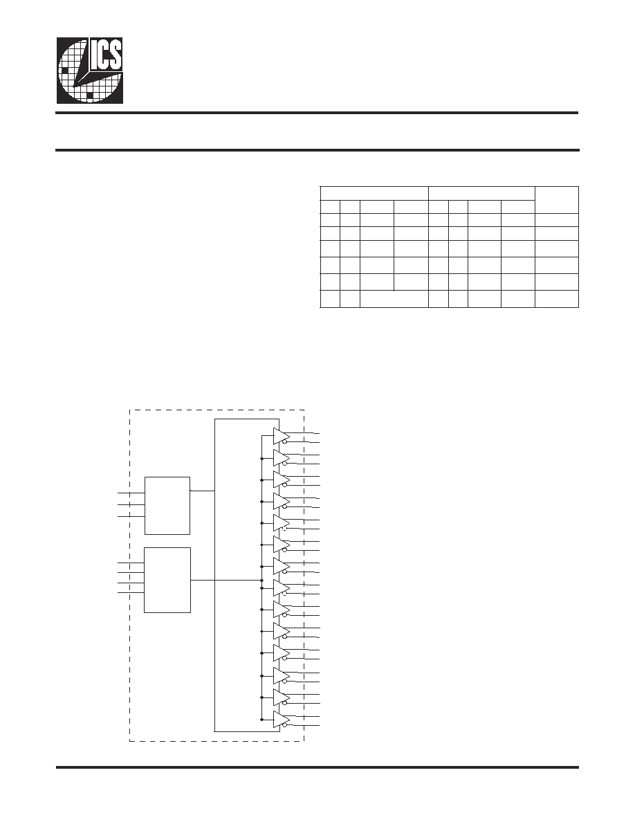
PLL
FB_INT
FB_INC
CLK_INC
CLK_INT
PD#
I2C_SCL, I2C_SDA
I2C_A0, I2CA1
Control
Logic
FB_OUTT
FB_OUTC
CLKT0
CLKT1
CLKT2
CLKT3
CLKT4
CLKT5
CLKT6
CLKT7
CLKT8
CLKT9
CLKC0
CLKC1
CLKC2
CLKC3
CLKC4
CLKC5
CLKC6
CLKC7
CLKC8
CLKC9
CLKT10
CLKT11
CLKC10
CLKC11
CLKT12
CLKC12
Block Diagram
2.5V DDR/Zero Delay Fan Out Buffer (100MHz - 225MHz)
Recommended Application:
DDR Memory Modules / Zero Delay Fan Out Buffer
Product Description/Features:
∑
Low skew, low jitter PLL clock driver
∑
1 to 13 differential clock distribution (SSTL_2)
∑
Feedback pins for input to output synchronization
∑
PD# for power management
∑
Spread Spectrum-tolerant inputs
∑
Auto PD when input signal removed
∑
0∞C to 85∞C operation
Switching Characteristics:
∑
CYCLE - CYCLE jitter (>100MHz):<75ps
∑
OUTPUT - OUTPUT skew: <70ps
∑
DUTY CYCLE: 49% - 51%
S
T
U
P
N
I
S
T
U
P
T
U
O
e
t
a
t
S
L
L
P
D
D
V
A
#
D
P
T
N
I
_
K
L
C
C
N
I
_
K
L
C
T
K
L
C
C
K
L
C
T
T
U
O
_
B
F
C
T
U
O
_
B
F
D
N
G
H
L
H
L
H
L
H
f
f
o
/
d
e
s
s
a
p
y
B
D
N
G
H
H
L
H
L
H
L
f
f
o
/
d
e
s
s
a
p
y
B
V
5
.
2
)
m
o
n
(
L
X
X
Z
Z
Z
Z
f
f
o
V
5
.
2
)
m
o
n
(
H
L
H
L
H
L
H
n
o
V
5
.
2
)
m
o
n
(
H
H
L
H
L
H
L
n
o
V
5
.
2
)
m
o
n
(
X
)
z
H
M
0
2
<
Z
Z
Z
Z
f
f
o
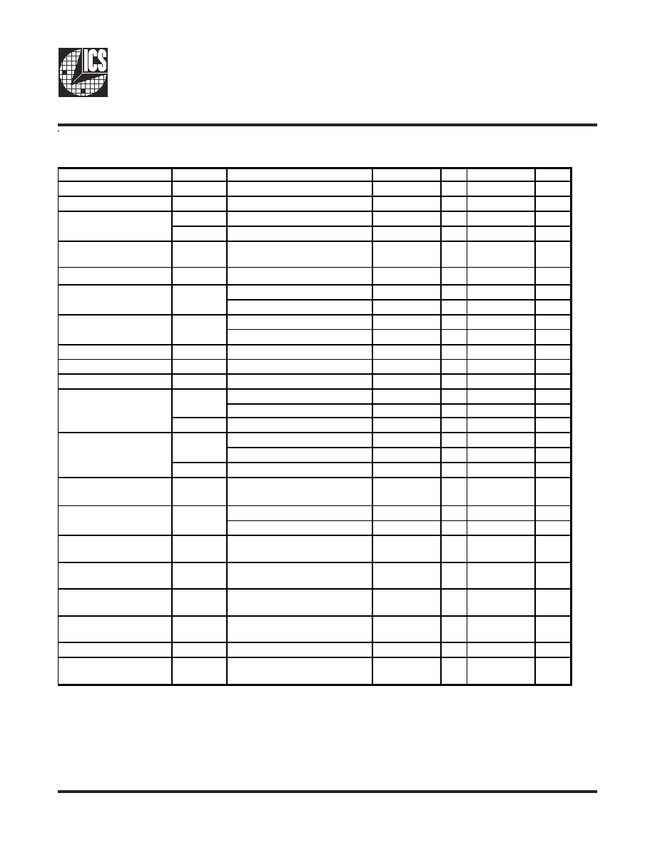
Functionality
2
ICS95V860
0675D--01/07/04
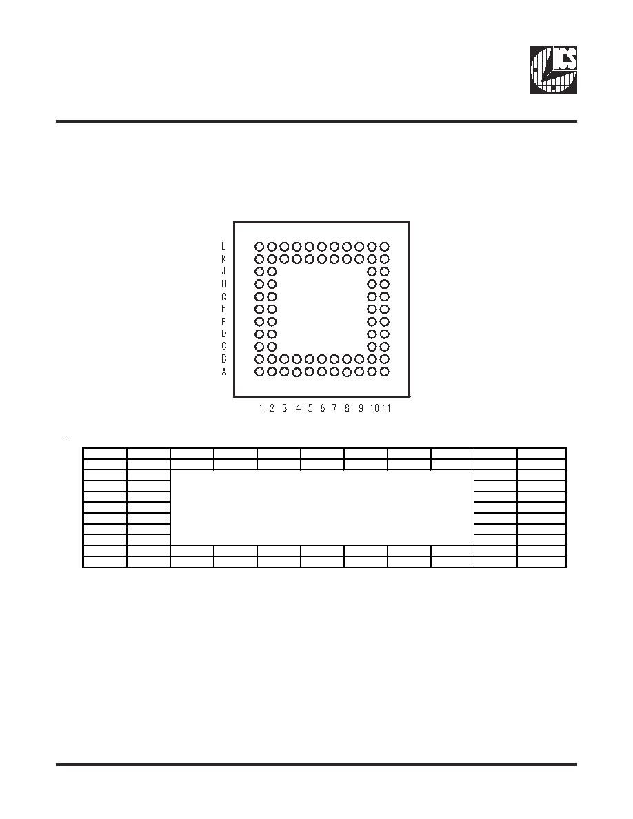
Bottom View
1
2
3
4
5
6
7
8
9
10
11
A
I2C_A0
CLKC0
CLKT0
CLKC1
CLKT1
CLKC2
CLKT2
CLKC3
CLKT3
PD#
VSS
B
I2C_A1
VSS
VDD
VDD
VSS
VSS
VDD
VDD
VSS
VSS
CLKC4
C FB_OUTT
VSS
VDD
CLKT4
D FB_OUTC
VDD
VDD
CLKC5
E
FB_INT
FB_INC
VSS
CLKT5
F
AVDD
AGND
VSS
CLKC6
G
CLK_INT
CLK_INC
VDD
CLKT6
H
CLKT12
VDD
VDD
CLKC7
J
CLKC12
VSS
VSS
CLKT7
K
I2C_SDA
VSS
VDD
VDD
VSS
VSS
VDD
VDD
VSS
VSS
VSS
L
I2C_SCL
CLKT11
CLKC11
CLKT10
CLKC10
CLKT9
CLKC9
CLKT8
CLKC8
VDD_I2C
VSS
Top View
3
ICS95V860
0675D--01/07/04
Pin Descriptions
R
E
B
M
U
N
N
I
P
E
M
A
N
N
I
P
E
P
Y
T
N
O
I
T
P
I
R
C
S
E
D
,
8
B
,
7
B
,
4
B
,
3
B
,
0
1
D
,
2
D
,
0
1
C
,
3
K
,
0
1
H
,
2
H
,
0
1
G
8
K
,
7
K
,
4
K
D
D
V
R
W
P
V
5
.
2
y
l
p
p
u
s
r
e
w
o
P
,
6
B
,
5
B
,
2
B
,
1
1
A
,
0
1
E
,
2
C
,
0
1
B
,
9
B
,
2
K
,
0
1
J
,
2
J
,
0
1
F
,
0
1
K
,
9
K
,
6
K
,
5
K
1
1
L
,
1
1
K
D
N
G
R
W
P
d
n
u
o
r
G
1
F
D
D
V
A
R
W
P
V
5
.
2
,
y
l
p
p
u
s
r
e
w
o
p
g
o
l
a
n
A
2
F
D
N
G
A
R
W
P
.
d
n
u
o
r
g
g
o
l
a
n
A
0
1
L
C
2
I
_
D
D
V
R
W
P
.
s
a
i
b
L
C
S
,
A
D
S
_
C
2
I
r
o
f
n
i
p
D
D
V
C
2
I
,
9
A
,
7
A
,
5
A
,
3
A
,
1
1
G
,
1
1
E
,
1
1
C
,
6
L
,
4
L
,
2
L
,
1
1
J
1
H
,
8
L
)
0
:
2
1
(
T
K
L
C
T
U
O
.
s
t
u
p
t
u
o
r
i
a
p
l
a
i
t
n
e
r
e
f
f
i
d
f
o
k
c
o
l
C
"
e
u
r
T
"
,
8
A
,
6
A
,
4
A
,
2
A
,
1
1
F
,
1
1
D
,
1
1
B
,
7
L
,
5
L
,
3
L
,
1
1
H
1
J
,
9
L
)
0
:
2
1
(
C
K
L
C
T
U
O
.
s
t
u
p
t
u
o
r
i
a
p
l
a
i
t
n
e
r
e
f
f
i
d
f
o
s
k
c
o
l
c
"
y
r
a
t
n
e
m
e
l
p
m
o
C
"
2
G
C
N
I
_
K
L
C
N
I
t
u
p
n
i
k
c
o
l
c
e
c
n
e
r
e
f
e
r
"
y
r
a
t
n
e
m
e
l
p
m
o
C
"
1
G
T
N
I
_
K
L
C
N
I
t
u
p
n
i
k
c
o
l
c
e
c
n
e
r
e
f
e
r
"
e
u
r
T
"
1
D
C
T
U
O
_
B
F
T
U
O
t
I
.
k
c
a
b
d
e
e
f
l
a
n
r
e
t
x
e
r
o
f
d
e
t
a
c
i
d
e
d
,
t
u
p
t
u
o
k
c
a
b
d
e
e
F
"
y
r
a
t
n
e
m
e
l
p
m
o
C
"
d
e
r
i
w
e
b
t
s
u
m
t
u
p
t
u
o
s
i
h
T
.
K
L
C
e
h
t
s
a
y
c
n
e
u
q
e
r
f
e
m
a
s
e
h
t
t
a
s
e
h
c
t
i
w
s
.
C
N
I
_
B
F
o
t
1
C
T
T
U
O
_
B
F
T
U
O
s
e
h
c
t
i
w
s
t
I
.
k
c
a
b
d
e
e
f
l
a
n
r
e
t
x
e
r
o
f
d
e
t
a
c
i
d
e
d
,
t
u
p
t
u
o
k
c
a
b
d
e
e
F
"
"
e
u
r
T
"
o
t
d
e
r
i
w
e
b
t
s
u
m
t
u
p
t
u
o
s
i
h
T
.
K
L
C
e
h
t
s
a
y
c
n
e
u
q
e
r
f
e
m
a
s
e
h
t
t
a
.
T
N
I
_
B
F
1
E
T
N
I
_
B
F
N
I
r
o
f
L
L
P
l
a
n
r
e
t
n
i
e
h
t
o
t
l
a
n
g
i
s
k
c
a
b
d
e
e
f
s
e
d
i
v
o
r
p
,
t
u
p
n
i
k
c
a
b
d
e
e
F
"
e
u
r
T
"
.
r
o
r
r
e
e
s
a
h
p
e
t
a
n
i
m
il
e
o
t
T
N
I
_
K
L
C
h
t
i
w
n
o
i
t
a
z
i
n
o
r
h
c
n
y
s
2
E
C
N
I
_
B
F
N
I
L
L
P
l
a
n
r
e
t
n
i
e
h
t
o
t
l
a
n
g
i
s
s
e
d
i
v
o
r
p
,
t
u
p
n
i
k
c
a
b
d
e
e
F
"
y
r
a
t
n
e
m
e
l
p
m
o
C
"
.
r
o
r
r
e
e
s
a
h
p
e
t
a
n
i
m
il
e
o
t
C
N
I
_
K
L
C
h
t
i
w
n
o
i
t
a
z
i
n
o
r
h
c
n
y
s
r
o
f
0
1
A
#
D
P
N
I
t
u
p
n
i
S
O
M
C
V
L
.
n
w
o
D
r
e
w
o
P
1
B
,
1
A
1
A
_
C
2
I
,
0
A
_
C
2
I
N
I
.
s
t
i
b
s
s
e
r
d
d
a
C
2
I
1
K
A
D
S
_
C
2
I
N
I
.
e
n
il
a
t
a
d
s
u
b
C
2
I
1
L
L
C
S
_
C
2
I
N
I
.
e
n
il
k
c
o
l
c
s
u
b
C
2
I
ICS95V860 is a zero delay buffer that distributes a differential clock input pair (CLK_INC, CLK_INT) to thirteen
differential clock output pairs (CLKT[0:12], CLKC[0:12]) and one differential clock output feedback pair (FB_OUT,
FB_OUTC). The clock outputs are controlled by the input clocks (CLK_INC, CLK_INT), the feedback clocks (FB_INT,
FB_INC) the input (PD#) and the Analog Power input (AV
DD
). When input (PD#) is low while power is applied, the receivers
are disabled, the PLL is turned off and the differential clock outputs are Tri-Stated. When AV
DD
is grounded, the PLL
is turned off and bypassed for test purposes.
When the input frequency is less than the operating frequency of the PLL (appproximately 20MHz), the device will enter
a low power mode. An input frequency detection circuit on the differential inputs, independent from the input buffers,
will detect the low frequency condition and perform the same low power features as when the (PD#) input is low. When
the input frequency increases to greater than approximately 20 MHz, the PLL will be turned back on, the inputs and
outputs will be enabled and PLL will obtain phase lock between the feedback clock pair (FB_INT, FB_INC) and the input
clock pair (CLK_INC, CLK_INT).
General Description
(continued)
4
ICS95V860
0675D--01/07/04
Absolute Maximum Ratings
Supply Voltage (VDD & AVDD) . . . . . . . . . . . -0.5V to 3.6V
Logic Inputs (except SDA, SCL) . . . . . . . . . GND ≠0.5 V to V
DD
+ 0.5 V
Logic Inputs (SDA, SCL) . . . . . . . . . . . . . . . GND ≠0.5 V to V
DDI2C
+ 0.6 V
Ambient Operating Temperature . . . . . . . . . . 0∞C to +85∞C
Storage Temperature . . . . . . . . . . . . . . . . . . . ≠65∞C to +150∞C
Stresses above those listed under
Absolute Maximum Ratings may cause permanent damage to the device. These
ratings are stress specifications only and functional operation of the device at these or any other conditions above those
listed in the operational sections of the specifications is not implied. Exposure to absolute maximum rating conditions
for extended periods may affect product reliability.
The ICS95V860 is able to track Spread Spectrum Clock (SSC) for reduced EMI.
The ICS95V860 is an I
2
C slave/receiver that supports standard and "fast" mode. The ICS95V860 I
2
C interface is
compliant to "The I2C-Bus Specification", version 2.1 January 2000 Philips Semiconductors, except that I2C_SDA
and I2C_SCL are not 5.0V tolerant, but have a maximum input voltage of 4.2V or V
DDI2C
+ 0.6V, whichever is
lower. Register bits control the enable for each output pair and a global enable bit (GLOBALEN#) disables all
outputs except the feeback output pair. A low places the disabled output pair in a high impedance state. Outputs
are active during power up and are guaranteed to be at the correct duty cycle and period after the clock
stabilization time.
General Description (Continued)
Device I2C address = 11001, A1, A0, R/W
I
2
C Table: Output Control Register
Control
Function
Bit 7
CLK0EN
Output Control
RW
1
Bit 6
CLK1EN
Output Control
RW
1
Bit 5
CLK2EN
Output Control
RW
1
Bit 4
CLK3EN
Output Control
RW
1
Bit 3
CLK4EN
Output Control
RW
1
Bit 2
CLK5EN
Output Control
RW
1
Bit 1
CLK6EN
Output Control
RW
1
Bit 0
CLK7EN
Output Control
RW
1
I
2
C Table: Output Control Register
Control
Function
Bit 7
CLK8EN
Output Control
RW
1
Bit 6
CLK9EN
Output Control
RW
1
Bit 5
CLK10EN
Output Control
RW
1
Bit 4
CLK11EN
Output Control
RW
1
Bit 3
CLK12EN
Output Control
RW
1
Bit 2
Reserved
Reserved
RW
0
Bit 1
Reserved
Reserved
RW
0
Bit 0
GLOBALEN#
Output Control
RW
0
NOTE: GLOBALEN# does not tristate the feedback output pair. The PLL continues to run and maintains lock even though all other outputs are tri-stated
Disable = Output in high-impedance state
Enable
0
1
Enable
Enable
Disable
A6,A7
PWD
A2,A3
A4,A5
Byte 0
Pin #
Name
Type
Disable
Disable
H11,J11
Byte 1
Pin #
A8,A9
B11,C11
D11,E11
F11,G11
Disable
Enable
Disable
Enable
Disable
Enable
Disable
Disable
Enable
Enable
PWD
L8,L9
Disable
Enable
Name
Type
0
1
L6,L7
Disable
Enable
L4,L5
Disable
Enable
L2,L3
Disable
Enable
H1,J1
Disable
Enable
-
Enable
Disable
-
-
-
-
-
-
5
ICS95V860
0675D--01/07/04
Notes:
1.
Unused inputs must be held high or low to prevent them from floating.
2.
DC input signal voltage specifies the allowable DC execution of differential input.
3.
Differential inputs signal voltages specifies the differential voltage [VT-VC]
required for switching, where VT is the true input level and VC is the
complementary input level.
4.
Guaranteed by design, not 100% tested in production.
Electrical Characteristics - Input/Supply/Common Output Parameters
T
A
= 0 - 85∞C; Supply Voltage A
VDD
, V
DD
= 2.5 V +/- 0.2V (unless otherwise stated)
PARAMETER
SYMBOL
CONDITIONS
MIN
TYP
MAX
UNITS
Input High Current
I
IH
V
I
= V
DD
or GND
5
µA
Input Low Current
I
IL
V
I
= V
DD
or GND
5
µA
I
DD2.5
C
L
= 0pf @ 200MHz
250
290
mA
I
DDPD
Enable = Low, F
IN
= 0 MHz
200
µA
High Impedance
Output Current
I
OZ
V
DD
= 2.7V, Vout=V
DD
or GND
±10
µA
Input Clamp Voltage
V
IK
V
DDQ
= 2.3V Iin = -18mA
-1.2
V
I
OH
= -1 mA
V
DD
- 0.1
V
I
OH
= -12 mA
1.7V
V
I
OL
=1 mA
0.1
V
I
OL
=12 mA
0.6
V
Input Capacitance
4
C
IN
V
I
= GND or V
DD
2.5
3.5
pF
Supply Voltage
V
DDQ
, A
VDD
2.3
2.7
V
I2C Supply Voltage
V
DD_I2C
I2C VDD supply pin
2.3
3.6
V
CLKT, CLKC, FB_INC
V
DDQ
/2 - 0.18
V
PD#, I2C_A0, I2C_A1
-0.3
0.7
V
V
IL_I2C
I2C_SDA, I2C_SCL
-0.3
0.3 x V
DD_I2C
V
CLKT, CLKC, FB_INC
V
DDQ
/2 + 0.18
V
PD#
1.7
V
DDQ
+ 0.6
V
V
IH_I2C
I2C_SDA, I2C_SCL
0.7 x V
DD_I2C
V
DD_I2C
+ 0.6
V
DC input signal voltage
2
-0.3
V
DDQ
V
DC - CLKT, FB_INT
0.36
V
DDQ
+ 0.6
V
AC - CLKT, FB_INT
0.7
V
DDQ
+ 0.6
V
Output differential cross-
voltage
V
OX
V
DDQ
/2 - 0.15
V
DDQ
/2 + 0.15
V
Input differential cross-
voltage
V
IX
V
DDQ
/2 - 0.2
V
DDQ
/2 + 0.2
V
High level output
current
I
OH
V
OH
= 1.7V
-12
mA
Low level output current
I
OL
V
OL
= 0.6V
12
mA
Input slew rate
S
R
1
4
V/ns
Operating free-air
temperature
T
A
0
85
∞C
Differential input signal
voltage
3
V
ID
Low level input voltage
V
IL
High level input voltage
V
IH
Operating Supply
Current
High-level output
voltage
V
OH
Low-level output voltage
V
OL