 | ÐлекÑÑоннÑй компоненÑ: ICS9DB102 | СкаÑаÑÑ:  PDF PDF  ZIP ZIP |
Äîêóìåíòàöèÿ è îïèñàíèÿ www.docs.chipfind.ru
Integrated
Circuit
Systems, Inc.
ICS9DB102
0852BC--09/12/05
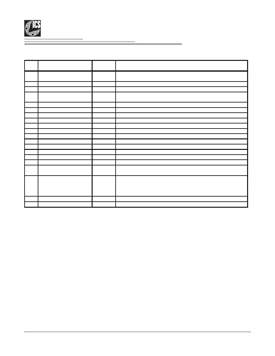
Pin Configuration
Recommended Application:
·
1-to-2 Zero-delay or fanout buffer for PCI Express
Output Features:
·
2 - 0.7V current mode differential output pairs (HSCL)
Key Specifications:
·
Cycle-to-cycle jitter < 35ps
·
Output-to-output skew < 25 ps
Features/Benefits:
·
CLKREQ# pin for outputs 1 and 4/output enable for
Express Card applications
·
PLL or bypass mode/PLL can dejitter incoming clock
·
Selectable PLL bandwidth/minimizes jitter peaking in
downstream PLL's
·
Spread Spectrum Compatible/tracks spreading input
clock for low EMI
·
SMBus Interface/unused outputs can be disabled
2 Output PCI Express* Buffer with CLKREQ# Function
20-pin SSOP & TSSOP
*Other names and brands may be claimed as the property of others.
PLL_BW 1
20 VDDA
CLK_INT 2
19 GNDA
CLK_INC 3
18 IREF
**CLKREQ0# 4
17 **CLKREQ1#
VDD 5
16 VDD
GND 6
15 GND
PCIEXT0 7
14 PCIEXT1
PCIEXC0 8
13 PCIEXC1
VDD 9
12 VDD
SMBDAT 10
11 SMBCLK
I
C
S
9
DB10
2
Note: Pins preceeded by '**' have internal
120K ohm pull down resistors
2
Integrated
Circuit
Systems, Inc.
ICS9DB102
0852C--09/12/05
Pin Description
PIN #
PIN NAME
PIN TYPE
DESCRIPTION
1
PLL_BW
IN
3.3V input for selecting PLL Band Width
0 = low, 1= high
2
CLK_INT
IN
"True" reference clock input.
3
CLK_INC
IN
"Complementary" reference clock input.
4
**CLKREQ0#
IN
Output enable for SRC/PCI Express output pair '0'
0 = enabled, 1 = tri-stated
5
VDD
PWR
Power supply, nominal 3.3V
6
GND
PWR
Ground pin.
7
PCIEXT0
OUT
True clock of differential PCI_Express pair.
8
PCIEXC0
OUT
Complement clock of differential PCI_Express pair.
9
VDD
PWR
Power supply, nominal 3.3V
10
SMBDAT
I/O
Data pin of SMBUS circuitry, 5V tolerant
11
SMBCLK
IN
Clock pin of SMBUS circuitry, 5V tolerant
12
VDD
PWR
Power supply, nominal 3.3V
13
PCIEXC1
OUT
Complement clock of differential PCI_Express pair.
14
PCIEXT1
OUT
True clock of differential PCI_Express pair.
15
GND
PWR
Ground pin.
16
VDD
PWR
Power supply, nominal 3.3V
17
**CLKREQ1#
IN
Output enable for SRC/PCI Express output pair '1'
0 = enabled, 1 = tri-stated
18
IREF
OUT
This pin establishes the reference current for the differential current-
mode output pairs. This pin requires a fixed precision resistor tied to
ground in order to establish the appropriate current. 475 ohms is the
standard value.
19
GNDA
PWR
Ground pin for the PLL core.
20
VDDA
PWR
3.3V power for the PLL core.
Pins preceeded by '**' have internal 120K ohm pull down resistors
Note:
3
Integrated
Circuit
Systems, Inc.
ICS9DB102
0852C--09/12/05
The ICS9DB102 zero-delay buffer supports PCI Express clocking requirements. The ICS9DB102 is driven by a differential
SRC output pair from an ICS CK409/CK410-compliant main clock generator such as the ICS952601 or ICS954101. It
attenuates jitter on the input clock and has a selectable PLL Band Width to maximize performance in systems with or without
Spread-Spectrum clocking. An SMBus interface allows control of the PLL bandwidth and bypass options, while 2 clock
request (OE#) pins make the ICS9DB102 suitable for Express Card applications.
General Description
Block Diagram
Power Groups
SPREAD
COMPATIBLE
PLL
CONTROL
LOGIC
SMBDAT
SMBCLK
CLK_INT
C LK_IN C
PLL_BW
IREF
PCIEX0
PCIEX1
CLKREQ1#
CLKREQ0#
VDD
GND
5,9,12,16
6,15
PCI Express Outputs
9
6
SMBUS
20
19
IREF
20
19
Analog VDD & GND for PLL core
Description
Pin Number
4
Integrated
Circuit
Systems, Inc.
ICS9DB102
0852C--09/12/05
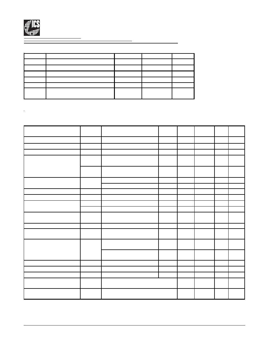
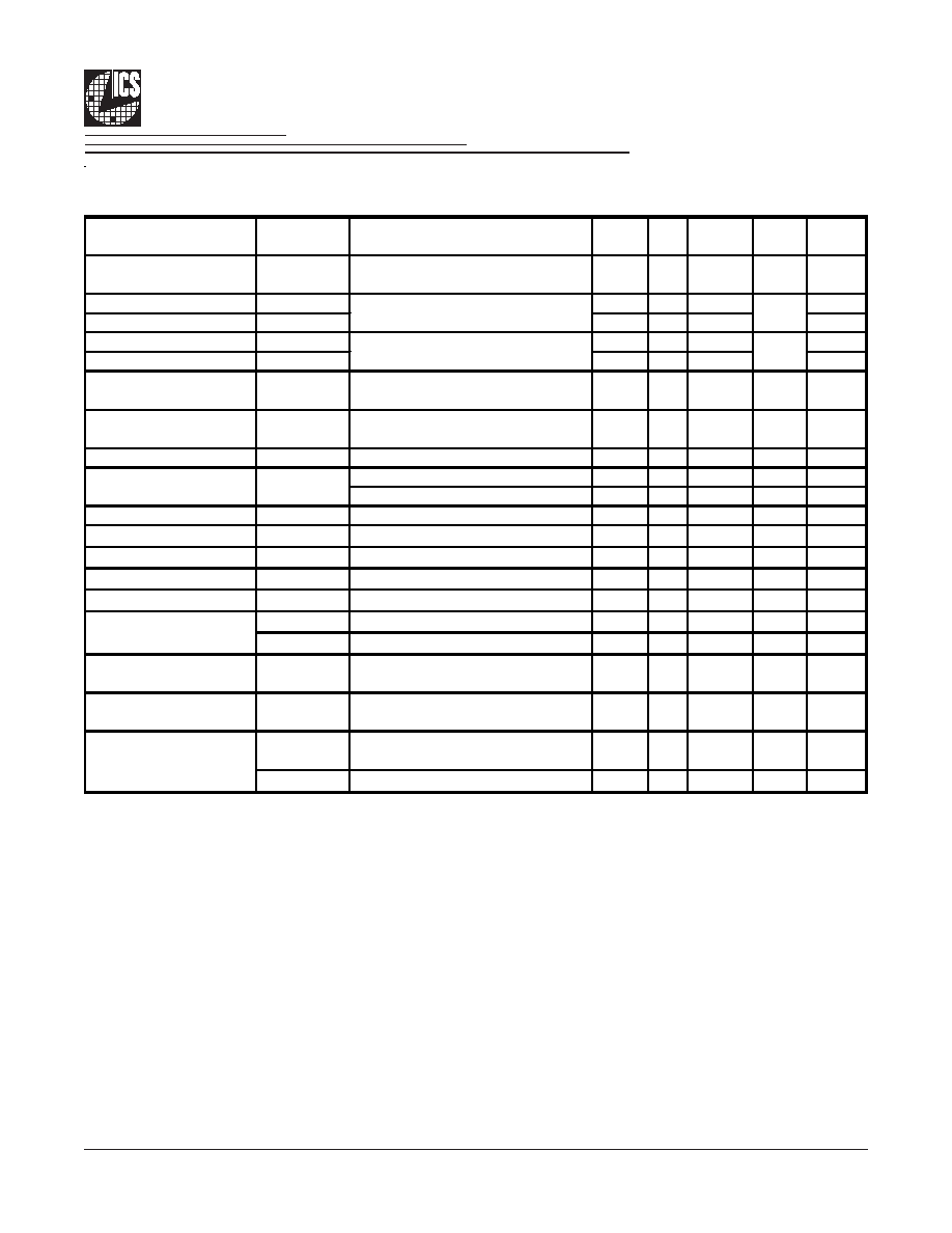
Absolute Max
Symbol
Parameter
Min
Max
Units
VDDA
3.3V Core Supply Voltage
V
DD
+ 0.5V
V
VDD
3.3V Output Supply Voltage
GND - 0.5
V
DD
+ 0.5V
V
Ts
Storage Temperature
-65
150
°
C
Tambient
Ambient Operating Temp
0
70
°C
Tcase Case
Temperature
115
°C
ESD prot
Input ESD protection
human body model
2000
V
Electrical Characteristics - Input/Supply/Common Output Parameters
T
A
= 0 - 70°C; Supply Voltage V
DD
= 3.3 V +/-5%
PARAMETER
SYMBOL
CONDITIONS
MIN
TYP
MAX
UNITS NOTES
Input High Voltage
V
IH
3.3 V +/-5%
2
V
DD
+ 0.3
V
1
Input Low Voltage
V
IL
3.3 V +/-5%
V
SS
- 0.3
0.8
V
1
Input High Current
I
IH
V
IN
= V
DD
-5
5
uA
1
I
IL1
V
IN
= 0 V; Inputs with no pull-
up resistors
-5
uA
1
I
IL2
V
IN
= 0 V; Inputs with pull-up
resistors
-200
uA
1
Full Active, C
L
= Full load;
75
100
mA
1
all differential pairs tri-stated
27
50
mA
1
Input Frequency
3
F
i
V
DD
= 3.3 V
99
100
101
MHz
1
Pin Inductance
1
L
pin
7
nH
1
C
IN
Logic Inputs
5
pF
1
C
OUT
Output pin capacitance
4.5
pF
1
Clk Stabilization
1,2
T
STAB
From V
DD
Power-Up to 1st
clock
1.8
ms
1
Modulation Frequency
Triangular Modulation
30
33
kHz
1
Spread Spectrum Modulation
Frequency
f
MOD
Lexmark Modulation
25
45
KHz
1
PLL Bandwidth when
PLL_BW=0
400
KHz
1
PLL Bandwidth when
PLL_BW=1
1.2
MHz
1
SMBus Voltage
V
DD
2.7
5.5
V
1
Low-level Output Voltage
V
OLSMBUS
@ I
PULLUP
0.4
V
1
Current sinking at V
OL
= 0.4 V
I
PULLUP
SMBus SDATA pin
4
mA
1
SCLK/SDATA
Clock/Data Rise Time
T
RI2C
(Max VIL - 0.15) to (Min VIH + 0.15)
1000
ns
1
SCLK/SDATA
Clock/Data Fall Time
T
FI2C
(Min VIH + 0.15) to (Max VIL - 0.15)
300
ns
1
1
Guaranteed by design and characterization, not 100% tested in production.
PLL Bandwidth
BW
Input Low Current
Input Capacitance
1
Operating Supply Current
I
DD3.3OP
5
Integrated
Circuit
Systems, Inc.
ICS9DB102
0852C--09/12/05
Electrical Characteristics - PCIEX 0.7V Current Mode Differential Pair
T
A
= 0 - 70°C; V
DD
= 3.3 V +/-5%; C
L
=2pF, R
S
=33.2
, R
P
=49.9
,
REF
= 475
PARAMETER
SYMBOL
CONDITIONS
MIN
TYP
MAX
UNITS NOTES
Current Source Output
Impedance
Zo
V
O
= V
x
3000
1
Voltage High
VHigh
660
850
1,3
Voltage Low
VLow
-150
150
1,3
Max Voltage
Vovs
1150
1,3
Min Voltage
Vuds
-300
1,3
Crossing Voltage (abs) Vcross(abs)
250
350
550
mV
1,3
Crossing Voltage (var)
d-Vcross
Variation of crossing over all
edges
12
140
mV
1,3
Long Accuracy
ppm
see Tperiod min-max values
0
ppm
1,2
100.00MHz nominal
9.9970
10.0030
ns
2
100.00MHz spread
9.9970
10.0533
ns
2
Absolute min period
Tabsmin
100.00MHz nominal/spread
9.8720
ns
1,2
Rise Time
t
r
V
OL
= 0.175V, V
OH
= 0.525V
175
700
ps
1
Fall Time
t
f
V
OH
= 0.525V V
OL
= 0.175V
175
700
ps
1
Rise Time Variation
d-t
r
30
125
ps
1
Fall Time Variation
d-t
f
30
125
ps
1
t
pd
PLL Mode.
135
185
ps
1
t
pdbyp
Bypass mode
3.2
3.7
ns
1
Duty Cycle
d
t3
Measurement from differential
wavefrom
45
55
%
1
Output-to-Output Skew
t
sk3
V
T
= 50%
25
ps
1
t
jcyc-cyc
PLL mode. Measurement from
differential wavefrom
35
ps
1
t
jcyc-cycbyp
Additve Jitter in Bypass Mode
30
ps
1
1
Guaranteed by design, not 100% tested in production.
.
3
I
REF
= V
DD
/(3xR
R
). For R
R
= 475
(1%), I
REF
= 2.32mA. I
OH
= 6 x I
REF
and V
OH
= 0.7V @ Z
O
=50
.
2
All Long Term Accuracy and Clock Period specifications are guaranteed with the assumption that the
input clock complies with CK409/CK410 accuracy requirements
Input to Output Delay
Jitter, Cycle to cycle
mV
Measurement on single ended
signal using absolute value.
mV
Average period
Tperiod
Statistical measurement on single
ended signal using oscilloscope