Integrated
Circuit
Systems, Inc.
ICS9DB108
0723D--01/08/04
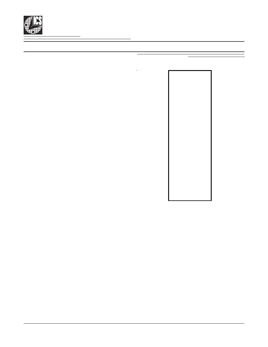
Pin Configuration
Recommended Application:
DB800 Intel Yellow Cover part with PCI-Express support.
Output Features:
∑
8 - 0.7V current-mode differential output pairs
∑
Supports zero delay buffer mode and fanout mode
∑
Bandwidth programming available
Key Specifications:
∑
Outputs cycle-cycle jitter < 50ps
∑
Outputs skew: 50ps
∑
+/- 300ppm frequency accuracy on output clocks
Features/Benefits:
∑
Supports tight ppm accuracy clocks for Serial-ATA
∑
Spread spectrum modulation tolerant, 0 to -0.5% down
spread and +/- 0.25% center spread
∑
Supports undriven differential output pair in PD# and
SRC_STOP# for power management.
Eight Output Differential Buffer for PCI-Express
48-pin SSOP & TSSOP
SRC_DIV#
1
48 VDDA
VDD
2
47 GNDA
GND
3
46 IREF
SRC_IN
4
45 LOCK
SRC_IN#
5
44 OE_7
OE_0
6
43 OE_4
OE_3
7
42 DIF_7
DIF_0
8
41 DIF_7#
DIF_0#
9
40 GND
GND 10
39 VDD
VDD 11
38 DIF_6
DIF_1 12
37 DIF_6#
DIF_1# 13
36 OE_6
OE_1 14
35 OE_5
OE_2 15
34 DIF_5
DIF_2 16
33 DIF_5#
DIF_2# 17
32 GND
GND 18
31 VDD
VDD 19
30 DIF_4
DIF_3 20
29 DIF_4#
DIF_3# 21
28 HIGH_BW#
BYPASS#/PLL 22
27 SRC_STOP#
SCLK 23
26 PD#
SDATA 24
25 GND
ICS9DB108

2
Integrated
Circuit
Systems, Inc.
ICS9DB108
0723D--01/08/04
Pin Description
PIN #
PIN NAME
PIN TYPE
DESCRIPTION
1
SRC_DIV#
IN
Active low Input for determining SRC output frequency SRC or
SRC/2.
0 = SRC/2, 1= SRC
2
VDD
PWR
Power supply, nominal 3.3V
3
GND
PWR
Ground pin.
4
SRC_IN
IN
0.7 V Differential SRC TRUE input
5
SRC_IN#
IN
0.7 V Differential SRC COMPLEMENTARY input
6
OE_0
IN
Active high input for enabling outputs.
0 = tri-state outputs, 1= enable outputs
7
OE_3
IN
Active high input for enabling outputs.
0 = tri-state outputs, 1= enable outputs
8
DIF_0
OUT
0.7V differential true clock outputs
9
DIF_0#
OUT
0.7V differential complement clock outputs
10
GND
PWR
Ground pin.
11
VDD
PWR
Power supply, nominal 3.3V
12
DIF_1
OUT
0.7V differential true clock outputs
13
DIF_1#
OUT
0.7V differential complement clock outputs
14
OE_1
IN
Active high input for enabling outputs.
0 = tri-state outputs, 1= enable outputs
15
OE_2
IN
Active high input for enabling outputs.
0 = tri-state outputs, 1= enable outputs
16
DIF_2
OUT
0.7V differential true clock outputs
17
DIF_2#
OUT
0.7V differential complement clock outputs
18
GND
PWR
Ground pin.
19
VDD
PWR
Power supply, nominal 3.3V
20
DIF_3
OUT
0.7V differential true clock outputs
21
DIF_3#
OUT
0.7V differential complement clock outputs
22
BYPASS#/PLL
IN
Input to select Bypass(fan-out) or PLL (ZDB) mode
0 = Bypass mode, 1= PLL mode
23
SCLK
IN
Clock pin of SMBus circuitry, 5V tolerant.
24
SDATA
I/O
Data pin for SMBus circuitry, 5V tolerant.

3
Integrated
Circuit
Systems, Inc.
ICS9DB108
0723D--01/08/04
Pin Description (Continued)
PIN #
PIN NAME
PIN TYPE
DESCRIPTION
25
GND
PWR
Ground pin.
26
PD#
IN
Asynchronous active low input pin used to power down the
device. The internal clocks are disabled and the VCO and the
crystal are stopped.
27
SRC_STOP#
IN
Active low input to stop diff outputs.
28
HIGH_BW#
PWR
3.3V input for selecting PLL Band Width
0 = High, 1= Low
29
DIF_4#
OUT
0.7V differential complement clock outputs
30
DIF_4
OUT
0.7V differential true clock outputs
31
VDD
PWR
Power supply, nominal 3.3V
32
GND
PWR
Ground pin.
33
DIF_5#
OUT
0.7V differential complement clock outputs
34
DIF_5
OUT
0.7V differential true clock outputs
35
OE_5
IN
Active high input for enabling outputs.
0 = tri-state outputs, 1= enable outputs
36
OE_6
IN
Active high input for enabling outputs.
0 = tri-state outputs, 1= enable outputs
37
DIF_6#
OUT
0.7V differential complement clock outputs
38
DIF_6
OUT
0.7V differential true clock outputs
39
VDD
PWR
Power supply, nominal 3.3V
40
GND
PWR
Ground pin.
41
DIF_7#
OUT
0.7V differential complement clock outputs
42
DIF_7
OUT
0.7V differential true clock outputs
43
OE_4
IN
Active high input for enabling outputs.
0 = tri-state outputs, 1= enable outputs
44
OE_7
IN
Active high input for enabling outputs.
0 = tri-state outputs, 1= enable outputs
45
LOCK
OUT
3.3V output indicating PLL Lock Status. This pin goes high when
lock is achieved.
46
IREF
IN
This pin establishes the reference current for the differential
current-mode output pairs. This pin requires a fixed precision
resistor tied to ground in order to establish the appropriate
current. 475 ohms is the standard value.
47
GNDA
PWR
Ground pin for the PLL core.
48
VDDA
PWR
3.3V power for the PLL core.
4
Integrated
Circuit
Systems, Inc.
ICS9DB108
0723D--01/08/04
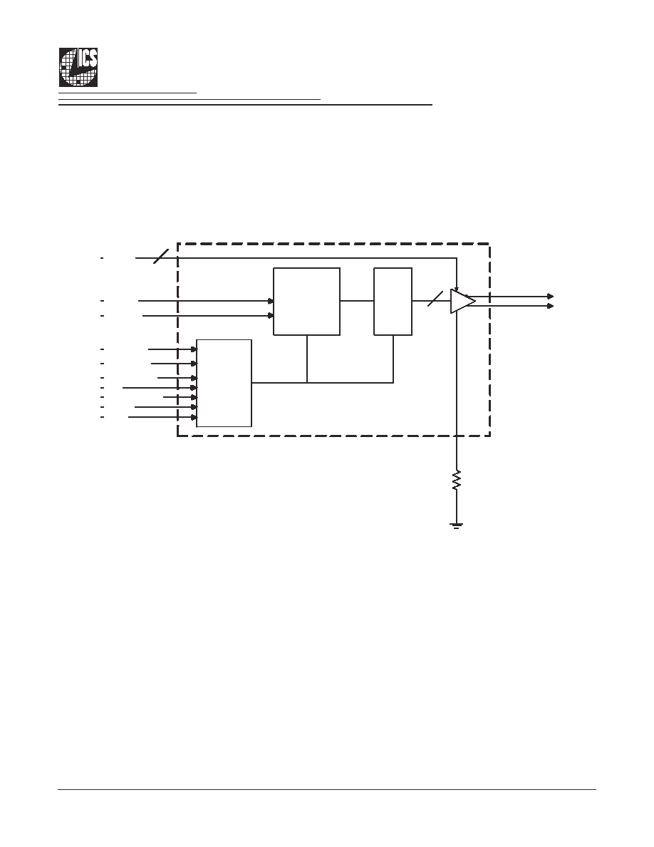
ICS9DB108 follows the Intel DB400 Differential Buffer Specification. This buffer provides four SRC clocks for PCI-Express,
next generation I/O devices. ICS9DB108 is driven by a differential input pair from a CK409/CK410 main clock generator, such
as the ICS952601 or ICS954101. ICS9DB108 can run at speeds up to 200MHz. It provides ouputs meeting tight cycle-to-cycle
jitter (50ps) and output-to-output skew (50ps) requirements.
General Description
Block Diagram
STOP
LOGIC
SRC_IN
SRC_IN#
DIF(7:0)
CONTROL
LOGIC
HIGH_BW#
BYPASS#/PLL
SDATA
SCLK
SRC_STOP#
PD#
SPREAD
COMPATIBLE
PLL
8
IREF
OE(7:0)
8
SRC_DIV#

5
Integrated
Circuit
Systems, Inc.
ICS9DB108
0723D--01/08/04
Absolute Max
Symbol
Parameter
Min
Max
Units
VDD_A
3.3V Core Supply Voltage
4.6
V
VDD_In
3.3V Logic Supply Voltage
4.6
V
V
IL
Input Low Voltage
GND-0.5
V
V
IH
Input High Voltage
V
DD
+0.5V
V
Ts
Storage Temperature
-65
150
∞
C
Tambient
Ambient Operating Temp
0
70
∞C
Tcase Case
Temperature
115
∞C
ESD prot
Input ESD protection
human body model
2000
V
Electrical Characteristics - Input/Supply/Common Output Parameters
T
A
= 0 - 70∞C; Supply Voltage V
DD
= 3.3 V +/-5%
PARAMETER
SYMBOL
CONDITIONS
MIN
TYP
MAX
UNITS NOTES
Input High Voltage
V
IH
3.3 V +/-5%
2
V
DD
+ 0.3
V
Input Low Voltage
V
IL
3.3 V +/-5%
GND
- 0.3
0.8
V
Input High Current
I
IH
V
IN
= V
DD
-5
5
uA
I
IL1
V
IN
= 0 V; Inputs with no pull-up
resistors
-5
uA
I
IL2
V
IN
= 0 V; Inputs with pull-up
resistors
-200
uA
Operating Supply Current
I
DD3.3OP
Full Active, C
L
= Full load;
250
mA
all diff pairs driven
60
mA
all differential pairs tri-stated
12
mA
Input Frequency
3
F
i
V
DD
= 3.3 V
80
100/133
166/200
220
MHz
3
Pin Inductance
1
L
pin
7
nH
1
C
IN
Logic Inputs
1.5
5
pF
1
C
OUT
Output pin capacitance
6
pF
1
PLL Bandwidth when
PLL_BW=0
4
MHz
1
PLL Bandwidth when
PLL_BW=1
2
MHz
1
Clk Stabilization
1,2
T
STAB
From V
DD
Power-Up and after
input clock stabilization or de-
assertion of PD# to 1st clock
1
ms
1,2
Modulation Frequency
Triangular Modulation
30
33
kHz
1
Tdrive_SRC_STOP#
DIF output enable after
SRC_Stop# de-assertion
10
ns
1,3
Tdrive_PD#
DIF output enable after
PD# de-assertion
300
us
1,3
Tfall
Fall time of PD# and
SRC_STOP#
5
ns
1
Trise
Rise time of PD# and
SRC_STOP#
5
ns
2
1
Guaranteed by design and characterization, not 100% tested in production.
2
See timing diagrams for timing requirements.
I
DD3.3PD
3
Time from deassertion until outputs are >200 mV
Input Capacitance
1
Input Low Current
Powerdown Current
PLL Bandwidth
BW

6
Integrated
Circuit
Systems, Inc.
ICS9DB108
0723D--01/08/04
Electrical Characteristics - DIF 0.7V Current Mode Differential Pair
T
A
= 0 - 70∞C; V
DD
= 3.3 V +/-5%; C
L
=2pF, R
S
=33.2
, R
P
=49.9
,
REF
= 475
PARAMETER
SYMBOL
CONDITIONS
MIN
TYP
MAX
UNITS
NOTES
Current Source Output
Impedance
Zo
1
V
O
= V
x
3000
1
Voltage High
VHigh
660
850
1,3
Voltage Low
VLow
-150
150
1,3
Max Voltage
Vovs
1150
1
Min Voltage
Vuds
-300
1
Crossing Voltage (abs) Vcross(abs)
250
550
mV
1
Crossing Voltage (var)
d-Vcross
Variation of crossing over all
edges
140
mV
1
Long Accuracy
ppm
see Tperiod min-max values
0
ppm
1,2
200MHz nominal
4.9985
5.0015
ns
2
200MHz spread
4.9985
5.0266
ns
2
166.66MHz nominal
5.9982
6.0018
ns
2
166.66MHz spread
5.9982
6.0320
ns
2
133.33MHz nominal
7.4978
7.5023
ns
2
133.33MHz spread
7.4978
5.4000
ns
2
100.00MHz nominal
9.9970
10.0030
ns
2
100.00MHz spread
9.9970
10.0533
ns
2
200MHz nominal
4.8735
ns
1,2
166.66MHz nominal/spread
5.8732
ns
1,2
133.33MHz nominal/spread
7.3728
ns
1,2
100.00MHz nominal/spread
9.8720
ns
1,2
Rise Time
t
r
V
OL
= 0.175V, V
OH
= 0.525V
175
700
ps
1
Fall Time
t
f
V
OH
= 0.525V V
OL
= 0.175V
175
700
ps
1
Rise Time Variation
d-t
r
125
ps
1
Fall Time Variation
d-t
f
125
ps
1
Duty Cycle
d
t3
Measurement from differential
wavefrom
45
55
%
1
Skew
t
sk3
V
T
= 50%
50
ps
1
PLL mode,
Measurement from differential
wavefrom
50
ps
1
BYPASS mode as additive jitter
50
ps
1
1
Guaranteed by design and characterization, not 100% tested in production.
3
I
REF
= V
DD
/(3xR
R
). For R
R
= 475
(1%), I
REF
= 2.32mA. I
OH
= 6 x I
REF
and V
OH
= 0.7V @ Z
O
=50
.
Statistical measurement on single
ended signal using oscilloscope
math function.
mV
Measurement on single ended
signal using absolute value.
mV
2
All Long Term Accuracy and Clock Period specifications are guaranteed with the assumption that the input clock
complies with CK409/CK410 accuracy requirements
Tperiod
Average period
Absolute min period
T
absmin
Jitter, Cycle to cycle
t
jcyc-cyc

7
Integrated
Circuit
Systems, Inc.
ICS9DB108
0723D--01/08/04
General SMBus serial interface information for the ICS9DB108
How to Write:
∑
Controller (host) sends a start bit.
∑ Controller (host) sends the write address DC
(H)
∑ ICS clock will
acknowledge
∑ Controller (host) sends the begining byte location = N
∑ ICS clock will
acknowledge
∑ Controller (host) sends the data byte count = X
∑ ICS clock will
acknowledge
∑ Controller (host) starts sending
Byte N through
Byte N + X -1
(see Note 2)
∑ ICS clock will
acknowledge each byte one at a time
∑ Controller (host) sends a Stop bit
How to Read:
∑ Controller (host) will send start bit.
∑ Controller (host) sends the write address DC
(H)
∑ ICS clock will
acknowledge
∑ Controller (host) sends the begining byte
location = N
∑ ICS clock will
acknowledge
∑ Controller (host) will send a separate start bit.
∑ Controller (host) sends the read address DD
(H)
∑ ICS clock will
acknowledge
∑ ICS clock will send the data byte count = X
∑ ICS clock sends
Byte N + X -1
∑ ICS clock sends
Byte 0 through byte X (if X
(H)
was written to byte 8)
.
∑ Controller (host) will need to acknowledge each byte
∑ Controllor (host) will send a not acknowledge bit
∑ Controller (host) will send a stop bit
ICS (Sla ve /Re ce ive r)
T
W R
ACK
ACK
ACK
ACK
ACK
P
stoP bit
X Byte
Index Block Write Operation
S lave Address DC
(H )
B eginning Byte = N
W Rite
starT bit
Controlle r (Host)
Byte N + X - 1
Data Byte Count = X
B eginning Byte N
T
starT bit
W R
W Rite
RT
Repeat starT
RD
ReaD
Beginning B yte N
Byte N + X - 1
N
Not acknowledge
P
stoP bit
ICS (Sla ve /Re ce ive r)
Controlle r (Host)
X Byte
ACK
ACK
Data Byte Count = X
ACK
S lave Address DD
(H )
Index Block Read Operation
S lave Address DC
(H )
B eginning Byte = N
ACK
ACK

8
Integrated
Circuit
Systems, Inc.
ICS9DB108
0723D--01/08/04
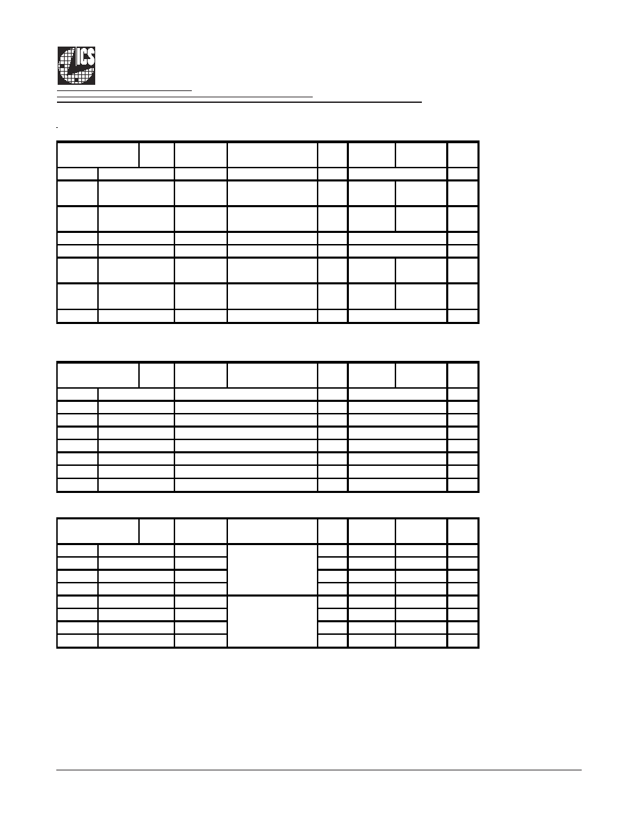
SMBus Table: Frequency Select Register, READ/WRITE ADDRESS (DC/DD)
Pin #
Name
Control Function Type
0
1
PWD
Bit 7
RW
driven
Hi-Z
0
Bit 6
RW
driven
Hi-Z
0
Bit 5
RW
X
Bit 4
RW
X
Bit 3
RW
X
Bit 2
RW
High BW
Low BW
1
Bit 1
RW
fan-out
ZDB
1
Bit 0
RW
x/2
1x
1
SMBus Table: Output Control Register
Pin #
Name
Control Function Type
0
1
PWD
Bit 7
DIF_7
Output Control
RW
Disable
Enable
1
Bit 6
DIF_6
Output Control
RW
Disable
Enable
1
Bit 5
DIF_5
Output Control
RW
Disable
Enable
1
Bit 4
DIF_4
Output Control
RW
Disable
Enable
1
Bit 3
DIF_3
Output Control
RW
Disable
Enable
1
Bit 2
DIF_2
Output Control
RW
Disable
Enable
1
Bit 1
DIF_1
Output Control
RW
Disable
Enable
1
Bit 0
DIF_0
Output Control
RW
Disable
Enable
1
Byte 0
-
PD# drive mode
-
SRC_Stop# drive mode
-
Reserved
Reserved
-
Reserved
Reserved
-
Reserved
Reserved
-
PLL_BW# adjust
-
BYPASS#/PLL
-
SRC_DIV#
Byte 1
42,41
38,37
34,33
30,29
20,21
16,17
12,13
8,9
9
Integrated
Circuit
Systems, Inc.
ICS9DB108
0723D--01/08/04
SMBus Table: Output Control Register
Pin #
Name
Control Function Type
0
1
PWD
Bit 7
DIF_7
Output Control
RW
0
Bit 6
DIF_6
Output Control
RW
Free-run Stoppable
0
Bit 5
DIF_5
Output Control
RW
Free-run Stoppable
0
Bit 4
DIF_4
Output Control
RW
0
Bit 3
DIF_3
Output Control
RW
0
Bit 2
DIF_2
Output Control
RW
Free-run Stoppable
0
Bit 1
DIF_1
Output Control
RW
Free-run Stoppable
0
Bit 0
DIF_0
Output Control
RW
0
SMBus Table: Output Control Register
Pin #
Name
Control Function Type
0
1
PWD
Bit 7
RW
X
Bit 6
RW
X
Bit 5
RW
X
Bit 4
RW
X
Bit 3
RW
X
Bit 2
RW
X
Bit 1
RW
X
Bit 0
RW
X
SMBus Table: Vendor & Revision ID Register
Pin #
Name
Control Function Type
0
1
PWD
Bit 7
RID3
R
-
-
0
Bit 6
RID2
R
-
-
0
Bit 5
RID1
R
-
-
0
Bit 4
RID0
R
-
-
1
Bit 3
VID3
R
-
-
0
Bit 2
VID2
R
-
-
0
Bit 1
VID1
R
-
-
0
Bit 0
VID0
R
-
-
1
Byte 2
42,41
38,37
34,33
30,29
20,21
16,17
Reserved
Reserved
12,13
8,9
Byte 3
Reserved
Reserved
Reserved
Reserved
Reserved
Reserved
Reserved
Reserved
Reserved
Reserved
Reserved
Reserved
Reserved
Byte 4
-
REVISION ID
-
-
-
-
VENDOR ID
-
-
-
Reserved
Reserved
Reserved
Reserved
Reserved

10
Integrated
Circuit
Systems, Inc.
ICS9DB108
0723D--01/08/04
SMBus Table: DEVICE ID
Pin #
Name
Control Function Type
0
1
PWD
Bit 7
RW
0
Bit 6
RW
0
Bit 5
RW
0
Bit 4
RW
0
Bit 3
RW
1
Bit 2
RW
0
Bit 1
RW
0
Bit 0
RW
0
SMBus Table: Byte Count Register
Pin #
Name
Control
Function
Type
0
1
PWD
Bit 7
BC7
RW
-
-
0
Bit 6
BC6
RW
-
-
0
Bit 5
BC5
RW
-
-
0
Bit 4
BC4
RW
-
-
0
Bit 3
BC3
RW
-
-
0
Bit 2
BC2
RW
-
-
1
Bit 1
BC1
RW
-
-
0
Bit 0
BC0
RW
-
-
1
-
-
-
-
-
Byte 5
-
-
-
Byte 6
-
Writing to this
register configures
how many bytes
will be read back.
-
-
-
-
-
-
-
Device ID 6
Reserved
Device ID 7 (MSB)
Reserved
Device ID 5
Reserved
Device ID 4
Reserved
Device ID 3
Reserved
Device ID 0
Reserved
Device ID 2
Reserved
Device ID 1
Reserved
11
Integrated
Circuit
Systems, Inc.
ICS9DB108
0723D--01/08/04
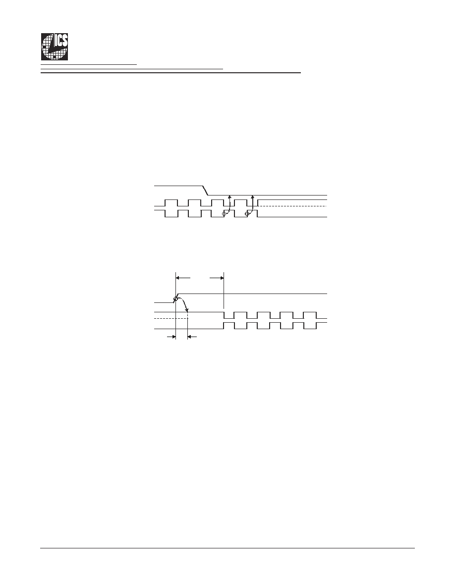
The PD# pin cleanly shuts off all clocks and places the device into a power saving mode. PD# must be asserted before
shutting off the input clock or power to insure an orderly shutdown. PD is asynchronous active-low input for both powering
down the device and powering up the device. When PD# is asserted, all clocks will be driven high, or tri-stated (depending
on the PD# drive mode and Output control bits) before the PLL is shut down.
PD#, Power Down
When PD# is sampled low by two consecutive rising edges of DIF#, all DIF outputs must be held High, or tri-stated (depending
on the PD# drive mode and Output control bits) on the next High-Low transition of the DIF# outputs. When the PD# drive mode
bit is set to `0', all clock outputs will be held with DIF driven High with 2 x I
REF
and DIF# tri-stated. If the PD# drive mode bit is
set to `1', both DIF and DIF# are tri-stated.
PD# Assertion
Power-up latency is less than 1 ms. This is the time from de-assertion of the PD# pin, or VDD reaching 3.3V, or the time from
valid SRC_IN clocks until the time that stable clocks are output from the device (PLL Locked). If the PD# drive mode bit is set
to `1', all the DIF outputs must driven to a voltage of >200 mV within 300 ms of PD# de-assertion.
PD# De-assertion
PWRDWN#
DIF
DIF#
PWRDWN#
DIF
DIF#
Tstable
<1mS
Tdrive_PwrDwn#
<300uS, >200mV
12
Integrated
Circuit
Systems, Inc.
ICS9DB108
0723D--01/08/04
Asserting SRC_STOP# causes all DIF outputs to stop after their next transition (if the control register settings allow the output
to stop). When the SRC_STOP# drive bit is `0', the final state of all stopped DIF outputs is DIF = High and DIF# = Low. There
is no change in output drive current. DIF is driven with 6xI
REF.
DIF# is not driven, but pulled low by the termination. When the
SRC_STOP# drive bit is `1', the final state of all DIF output pins is Low. Both DIF and DIF# are not driven.
SRC_STOP# - Assertion
All stopped differential outputs resume normal operation in a glitch-free manner. The de-assertion latency to active outputs is
2-6 DIF clock periods, with all DIF outputs resuming simultaneously. If the SRC_STOP# drive control bit is `1' (tri-state), all
stopped DIF outputs must be driven High (>200 mV) within 10 ns of de-assertion.
SRC_STOP# - De-assertion (transition from '0' to '1')
The SRC_STOP# signal is an active-low asynchronous input that cleanly stops and starts the DIF outputs. A valid clock must
be present on SRC_IN for this input to work properly. The SRC_STOP# signal is de-bounced and must remain stable for two
consecutive rising edges of DIF# to be recognized as a valid assertion or de-assertion.
SRC_STOP#
PWRDWN#
SRC_Stop#
DIF (Free Running)
DIF# (Free Running)
DIF (Stoppable)
DIF# (Stoppable)
1mS
PWRDWN#
SRC_Stop#
DIF (Free Running)
DIF# (Free Running)
DIF (Stoppable)
DIF# (Stoppable)
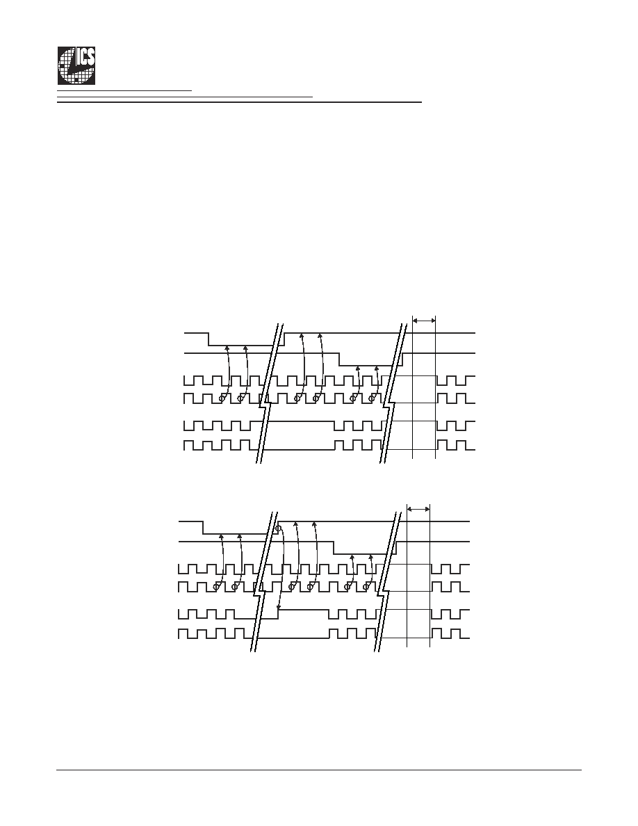
1mS
SRC_STOP_1 (SRC_Stop = Driven, PD = Driven)
SRC_STOP_2 (SRC_Stop =Tristate, PD = Driven)

13
Integrated
Circuit
Systems, Inc.
ICS9DB108
0723D--01/08/04
PWRDWN#
SRC_Stop#
DIF (Free Running)
DIF# (Free Running)
DIF (Stoppable)
DIF# (Stoppable)
1mS
PWRDWN#
SRC_Stop#
DIF (Free Running)
DIF# (Free Running)
DIF (Stoppable)
DIF# (Stoppable)
1mS
SRC_STOP_4 (SRC_Stop = Tristate, PD = Tristate)
SRC_STOP_3 (SRC_Stop = Driven, PD = Tristate)

14
Integrated
Circuit
Systems, Inc.
ICS9DB108
0723D--01/08/04
INDEX
AREA
INDEX
AREA
1 2
N
D
h x 45∞
E1
E
SEATING
PLANE
SEATING
PLANE
A1
A
e
- C -
b
.10 (.004) C
.10 (.004) C
c
L
MIN
MAX
MIN
MAX
A
2.41
2.80
.095
.110
A1
0.20
0.40
.008
.016
b
0.20
0.34
.008
.0135
c
0.13
0.25
.005
.010
D
E
10.03
10.68
.395
.420
E1
7.40
7.60
.291
.299
e
h
0.38
0.64
.015
.025
L
0.50
1.02
.020
.040
N
0∞
8∞
0∞
8∞
MIN
MAX
MIN
MAX
48
15.75
16.00
.620
.630
10-0034
SYMBOL
In Millimeters
In Inches
COMMON DIMENSIONS
COMMON DIMENSIONS
SEE VARIATIONS
SEE VARIATIONS
0.635 BASIC
0.025 BASIC
Reference Doc.: JEDEC Publication 95, MO-118
VARIATIONS
SEE VARIATIONS
SEE VARIATIONS
N
D mm.
D (inch)
Ordering Information
ICS9DB108yFLFT
Example:
Designation for tape and reel packaging
Lead Free (optional)
Package Type
F = SSOP
Revision Designator (will not correlate with datasheet revision)
Device Type (consists of 3 or 4 digit numbers)
Prefix
ICS, AV = Standard Device
ICS XXXX y F LF T

15
Integrated
Circuit
Systems, Inc.
ICS9DB108
0723D--01/08/04
INDEX
AREA
INDEX
AREA
1 2
1 2
N
D
E1
E
a
SEATING
PLANE
SEATING
PLANE
A1
A
A2
e
- C -
- C -
b
c
L
aaa
C
MIN
MAX
MIN
MAX
A
--
1.20
--
.047
A1
0.05
0.15
.002
.006
A2
0.80
1.05
.032
.041
b
0.17
0.27
.007
.011
c
0.09
0.20
.0035
.008
D
E
E1
6.00
6.20
.236
.244
e
L
0.45
0.75
.018
.030
N
a
0∞
8∞
0∞
8∞
aaa
--
0.10
--
.004
VARIATIONS
MIN
MAX
MIN
MAX
48
12.40
12.60
.488
.496
10-0039
Reference Doc.: JEDEC Publication 95, MO-153
In Millimeters
In Inches
COMMON DIMENSIONS
0.50 BASIC
0.020 BASIC
8.10 BASIC
0.319 BASIC
N
D (inch)
SEE VARIATIONS
SEE VARIATIONS
D mm.
48-Lead, 6.10 mm. Body, 0.50 mm. Pitch TSSOP
(240 mil) (20 mil)
SYMBOL
SEE VARIATIONS
COMMON DIMENSIONS
SEE VARIATIONS
Ordering Information
ICS9DB108yGLFT
Example:
Designation for tape and reel packaging
Lead Free (optional)
Package Type
G = TSSOP
Revision Designator (will not correlate with datasheet revision)
Device Type (consists of 3 or 4 digit numbers)
Prefix
ICS, AV = Standard Device
ICS XXXX y G LF T