Document Outline
- General Description
- Features
- Block Diagram
- Pin Assignment
- Pin Descriptions
- Pin Characteristics
- Ratio of Output Frequency to Input Frequency Function Table, FS0
- Ratio of Output Frequency to Input Frequency Function Table, FS1
- BYPASS Table
- Output Enable Function Table, nOE0
- Output Enable Function Table, nOE1
- PLL Bandwith Table
- Absolute Maximum Ratings
- Power Supply DC Characteristics
- LVCMOS DC Characteristics
- Differential DC Characteristics
- HCSL DC Characteristics
- AC Characteristics
- Typical Phase Noise Plot
- Parameter Measurement Information
- 3.3V HCSL Output Load AC Test Circuit Diagram
- Differential Input Level Diagram
- Output Skew Diagram
- Cycled-to-Cycle Jitter Diagram
- HCSL Output Rise/Fall Time Diagram
- Output Duty Cycle/Pulse Width/Period Diagram
- Application Information
- Power Supply Filtering Techniques
- Wiring the Differential Input to Accept Single Ended Levels
- Differential Clock Input Interface
- Reliability Information
- Transistor Count
- Package Outline for TSSOP
- Pakcage Dimensions for TSSOP
- Package Outline for SSOP
- Package Dimensions for SSOP
- Ordering Information

9DB202CG
www.icst.com/products/hiperclocks.html
REV. A OCTOBER 6, 2004
1
Integrated
Circuit
Systems, Inc.
ICS9DB202
PCI E
XPRESS
TM
J
ITTER
A
TTENUATOR
G
ENERAL
D
ESCRIPTION
The ICS9DB202 is a high perfromance 1-to-2 Dif-
ferential-to-HCSL Jitter Attenuator designed for use
in PCI ExpressTM systems. In some PCI ExpressTM
systems, such as those found in desktop PCs, the
PCI ExpressTM clocks are generated from a low
bandwidth, high phase noise PLL frequency synthesizer. In these
systems, a jitter-attenuating device may be necessary in order
to reduce high frequency random and deterministic jitter com-
ponents from the PLL synthesizer and from the system board.
The ICS9DB202 has two PLL bandwidth modes. In low band-
width mode, the PLL loop bandwidth is 500kHz. This setting of-
fers the best jitter attenuation and is still high enough to pass a
triangular input spread spectrum profile. In high bandwidth mode,
the PLL bandwidth is at 1MHz and allows the PLL to pass more
spread spectrum modulation.
For serdes which have x10 reference multipliers instead of x12.5
multipliers, each of the two PCI ExpressTM outputs (PCIEX0:1)
can be set for 125MHz instead of 100MHz by configuring the
appropriate frequency select pins (FS0:1).
Features
∑ Two 0.7V current mode differential HCSL output pairs
∑ 1 differential clock input
∑ CLK and nCLK supports the following input types:
LVPECL, LVDS, LVHSTL, SSTL, HCSL
∑ Maximum output frequency: 140MHz
∑ Output skew: 110ps (maximum)
∑ Cycle-to-cycle jitter: 110ps (maximum)
∑ RMS phase jitter @ 100MHz, (1.5MHz - 22MHz):
2.42ps (typical)
∑ 3.3V operating supply
∑ 0∞C to 70∞C ambient operating temperature
∑ Lead-Free package available
∑ Industrial temperature information available upon request
HiPerClockSTM
ICS
P
IN
A
SSIGNMENT
nOE0
nCLK
CLK
BYPASS
nOE1
PCIEXT0
nPCIEXC0
PCIEXT1
nPCIEXC1
B
LOCK
D
IAGRAM
ICS9DB202
20-Lead TSSOP
6.50mm x 4.40mm x 0.92
package body
G Package
Top View
ICS9DB202
20-Lead, 209-MIL SSOP
5.30mm x 7.20mm x 1.75mm
body package
F Package
Top View
Phase
Detector
VCO
Loop
Filter
1 HiZ
0 Enabled
1 HiZ
0 Enabled
0 ˜4
1 ˜5
0 ˜5
1 ˜4
FS0
FS1
Internal Feedback
˜5
Current
Set
-
+
0
1
0
1
IREF
PLL_BW
CLK
nCLK
FS0
V
DD
GND
PCIEXT0
PCIEXC0
V
DD
nOE0
1
2
3
4
5
6
7
8
9
10
20
19
18
17
16
15
14
13
12
11
V
DDA
BYPASS
IREF
FS1
V
DD
GND
PCIEXT1
PCIEXC1
V
DD
nOE1

9DB202CG
www.icst.com/products/hiperclocks.html
REV. A OCTOBER 6, 2004
2
Integrated
Circuit
Systems, Inc.
ICS9DB202
PCI E
XPRESS
TM
J
ITTER
A
TTENUATOR
T
ABLE
2. P
IN
C
HARACTERISTICS
T
ABLE
3A. R
ATIO
OF
O
UTPUT
F
REQUENCY
TO
I
NPUT
F
REQUENCY
F
UNCTION
T
ABLE
, FS0
l
o
b
m
y
S
r
e
t
e
m
a
r
a
P
s
n
o
i
t
i
d
n
o
C
t
s
e
T
m
u
m
i
n
i
M
l
a
c
i
p
y
T
m
u
m
i
x
a
M
s
t
i
n
U
C
N
I
e
c
n
a
t
i
c
a
p
a
C
t
u
p
n
I
4
F
p
R
P
U
L
L
U
P
r
o
t
s
i
s
e
R
p
u
ll
u
P
t
u
p
n
I
1
5
K
R
N
W
O
D
L
L
U
P
r
o
t
s
i
s
e
R
n
w
o
d
ll
u
P
t
u
p
n
I
1
5
K
s
t
u
p
n
I
s
t
u
p
t
u
O
0
S
F
0
X
E
I
C
P
0
4
/
5
1
1
T
ABLE
1. P
IN
D
ESCRIPTIONS
r
e
b
m
u
N
e
m
a
N
e
p
y
T
n
o
i
t
p
i
r
c
s
e
D
1
W
B
_
L
L
P
t
u
p
n
I
p
u
ll
u
P
.
s
l
e
v
e
l
e
c
a
f
r
e
t
n
i
L
T
T
V
L
/
S
O
M
C
V
L
.
t
u
p
n
i
h
t
d
i
w
d
n
a
B
L
L
P
s
t
c
e
l
e
S
2
K
L
C
t
u
p
n
I
n
w
o
d
ll
u
P
.
t
u
p
n
i
k
c
o
l
c
l
a
i
t
n
e
r
e
f
f
i
d
g
n
i
t
r
e
v
n
i
-
n
o
N
3
K
L
C
n
t
u
p
n
I
/
p
u
ll
u
P
n
w
o
d
ll
u
P
V
.
t
u
p
n
i
k
c
o
l
c
l
a
i
t
n
e
r
e
f
f
i
d
g
n
i
t
r
e
v
n
I
D
D
.
g
n
i
t
a
o
l
f
t
f
e
l
n
e
h
w
t
l
u
a
f
e
d
2
/
4
0
S
F
t
u
p
n
I
p
u
ll
u
P
.
s
l
e
v
e
l
e
c
a
f
r
e
t
n
i
L
T
T
V
L
/
S
O
M
C
V
L
.
n
i
p
t
c
e
l
e
s
y
c
n
e
u
q
e
r
F
6
1
,
2
1
,
9
,
5
V
D
D
r
e
w
o
P
.
s
n
i
p
y
l
p
p
u
s
e
r
o
C
5
1
,
6
D
N
G
r
e
w
o
P
.
d
n
u
o
r
g
y
l
p
p
u
s
r
e
w
o
P
8
,
7
,
0
T
X
E
I
C
P
0
C
X
E
I
C
P
t
u
p
t
u
O
.
s
l
e
v
e
l
e
c
a
f
r
e
t
n
i
L
S
C
H
.
s
r
i
a
p
t
u
p
t
u
o
l
a
i
t
n
e
r
e
f
f
i
D
1
1
,
0
1
1
E
O
n
,
0
E
O
n
t
u
p
n
I
n
w
o
d
ll
u
P
.
e
t
a
t
s
Z
i
H
o
t
s
t
u
p
t
u
o
s
e
c
r
o
f
,
H
G
I
H
n
e
h
W
.
e
l
b
a
n
e
t
u
p
t
u
O
.
s
l
e
v
e
l
e
c
a
f
r
e
t
n
i
L
T
T
V
L
/
S
O
M
C
V
L
.
s
t
u
p
t
u
o
s
e
l
b
a
n
e
,
W
O
L
n
e
h
W
4
1
,
3
1
,
1
C
X
E
I
C
P
1
T
X
E
I
C
P
t
u
p
t
u
O
.
s
l
e
v
e
l
e
c
a
f
r
e
t
n
i
L
S
C
H
.
s
r
i
a
p
t
u
p
t
u
o
l
a
i
t
n
e
r
e
f
f
i
D
7
1
1
S
F
t
u
p
n
I
n
w
o
d
ll
u
P
.
s
l
e
v
e
l
e
c
a
f
r
e
t
n
i
L
T
T
V
L
/
S
O
M
C
V
L
.
n
i
p
t
c
e
l
e
s
y
c
n
e
u
q
e
r
F
8
1
F
E
R
I
t
u
p
n
I
5
7
4
(
r
o
t
s
i
s
e
r
n
o
i
s
i
c
e
r
p
d
e
x
i
f
A
a
s
e
d
i
v
o
r
p
d
n
u
o
r
g
o
t
n
i
p
s
i
h
t
m
o
r
f
)
.
s
t
u
p
t
u
o
k
c
o
l
c
X
E
I
C
P
e
d
o
m
-
t
n
e
r
r
u
c
l
a
i
t
n
e
r
e
f
f
i
d
r
o
f
d
e
s
u
t
n
e
r
r
u
c
e
c
n
e
r
e
f
e
r
9
1
S
S
A
P
Y
B
r
e
w
o
P
n
w
o
d
ll
u
P
.
e
d
o
m
L
L
P
,
W
O
L
n
e
h
w
,
e
d
o
m
s
s
a
p
y
b
.
H
G
I
H
n
e
h
W
.
n
i
p
S
S
A
P
Y
B
.
s
l
e
v
e
l
e
c
a
f
r
e
t
n
i
L
T
T
V
L
/
S
O
M
C
V
L
0
2
V
A
D
D
r
e
w
o
P
4
2
s
e
r
i
u
q
e
R
.
n
i
p
y
l
p
p
u
s
g
o
l
a
n
A
.
r
o
t
s
i
s
e
r
s
e
i
r
e
s
:
E
T
O
N
p
u
ll
u
P
d
n
a
n
w
o
d
ll
u
P
.
s
e
u
l
a
v
l
a
c
i
p
y
t
r
o
f
,
s
c
i
t
s
i
r
e
t
c
a
r
a
h
C
n
i
P
,
2
e
l
b
a
T
e
e
S
.
s
r
o
t
s
i
s
e
r
t
u
p
n
i
l
a
n
r
e
t
n
i
o
t
r
e
f
e
r
T
ABLE
3B. R
ATIO
OF
O
UTPUT
F
REQUENCY
TO
I
NPUT
F
REQUENCY
F
UNCTION
T
ABLE
, FS1
s
t
u
p
n
I
s
t
u
p
t
u
O
1
S
F
1
X
E
I
C
P
0
1
1
4
/
5
T
ABLE
3D. O
UTPUT
E
NABLE
F
UNCTION
T
ABLE
,
N
OE0
s
t
u
p
n
I
s
t
u
p
t
u
O
0
E
O
n
0
X
E
I
C
P
0
d
e
l
b
a
n
E
1
Z
i
H
T
ABLE
3E. O
UTPUT
E
NABLE
F
UNCTION
T
ABLE
,
N
OE1
s
t
u
p
n
I
s
t
u
p
t
u
O
1
E
O
n
1
X
E
I
C
P
0
d
e
l
b
a
n
E
1
Z
i
H
T
ABLE
3F. PLL B
ANDWIDTH
T
ABLE
s
t
u
p
n
I
h
t
d
i
w
d
n
a
B
W
B
_
L
L
P
0
z
H
k
0
0
5
1
z
H
M
1
T
ABLE
3C. BYPASS T
ABLE
s
t
u
p
n
I
e
d
o
M
S
S
A
P
Y
B
0
e
d
o
M
L
L
P
1
e
d
o
M
s
s
a
p
y
B
)
s
t
u
p
n
i
=
t
u
p
t
u
o
(

9DB202CG
www.icst.com/products/hiperclocks.html
REV. A OCTOBER 6, 2004
3
Integrated
Circuit
Systems, Inc.
ICS9DB202
PCI E
XPRESS
TM
J
ITTER
A
TTENUATOR
T
ABLE
4C. D
IFFERENTIAL
DC C
HARACTERISTICS
,
V
DD
= V
DDA
= 3.3V±5%, T
A
= 0∞C
TO
70∞C, RREF = 475
l
o
b
m
y
S
r
e
t
e
m
a
r
a
P
s
n
o
i
t
i
d
n
o
C
t
s
e
T
m
u
m
i
n
i
M
l
a
c
i
p
y
T
m
u
m
i
x
a
M
s
t
i
n
U
I
H
I
t
n
e
r
r
u
C
h
g
i
H
t
u
p
n
I
K
L
C
n
,
K
L
C
V
D
D
V
=
N
I
V
5
6
4
.
3
=
0
5
1
A
µ
I
L
I
t
n
e
r
r
u
C
w
o
L
t
u
p
n
I
K
L
C
n
,
K
L
C
V
D
D
V
,
V
5
6
4
.
3
=
N
I
V
0
=
0
5
1
A
µ
V
P
P
e
g
a
t
l
o
V
t
u
p
n
I
k
a
e
P
-
o
t
-
k
a
e
P
5
1
.
0
3
.
1
V
V
R
M
C
2
,
1
E
T
O
N
;
e
g
a
t
l
o
V
t
u
p
n
I
e
d
o
M
n
o
m
m
o
C
5
.
0
+
D
N
G
V
D
D
5
8
.
0
-
V
V
s
a
d
e
n
i
f
e
d
s
i
e
g
a
t
l
o
v
e
d
o
m
n
o
m
m
o
C
:
1
E
T
O
N
H
I
.
V
s
i
K
L
C
n
,
K
L
C
r
o
f
e
g
a
t
l
o
v
t
u
p
n
i
m
u
m
i
x
a
m
e
h
t
,
s
n
o
i
t
a
c
il
p
p
a
d
e
d
n
e
e
l
g
n
i
s
r
o
F
:
2
E
T
O
N
D
D
.
V
3
.
0
+
T
ABLE
4A. P
OWER
S
UPPLY
DC C
HARACTERISTICS
,
V
DD
= V
DDA
= 3.3V±5%, T
A
= 0∞C
TO
70∞C, RREF = 475
T
ABLE
4B. LVCMOS / LVTTL DC C
HARACTERISTICS
,
V
DD
= V
DDA
= 3.3V±5%, T
A
= 0∞C
TO
70∞C
l
o
b
m
y
S
r
e
t
e
m
a
r
a
P
s
n
o
i
t
i
d
n
o
C
t
s
e
T
m
u
m
i
n
i
M
l
a
c
i
p
y
T
m
u
m
i
x
a
M
s
t
i
n
U
V
D
D
e
g
a
t
l
o
V
y
l
p
p
u
S
e
r
o
C
5
3
1
.
3
3
.
3
5
6
4
.
3
V
V
A
D
D
e
g
a
t
l
o
V
y
l
p
p
u
S
g
o
l
a
n
A
5
3
1
.
3
3
.
3
5
6
4
.
3
V
I
D
D
t
n
e
r
r
u
C
y
l
p
p
u
S
r
e
w
o
P
2
1
1
A
m
I
A
D
D
t
n
e
r
r
u
C
y
l
p
p
u
S
g
o
l
a
n
A
2
2
A
m
l
o
b
m
y
S
r
e
t
e
m
a
r
a
P
s
n
o
i
t
i
d
n
o
C
t
s
e
T
m
u
m
i
n
i
M
l
a
c
i
p
y
T
m
u
m
i
x
a
M
s
t
i
n
U
V
H
I
e
g
a
t
l
o
V
h
g
i
H
t
u
p
n
I
2
V
D
D
3
.
0
+
V
m
V
L
I
e
g
a
t
l
o
V
w
o
L
t
u
p
n
I
3
.
0
-
8
.
0
V
m
I
H
I
t
n
e
r
r
u
C
h
g
i
H
t
u
p
n
I
,
S
S
A
P
Y
B
1
S
F
,
1
E
O
n
,
0
E
O
n
V
D
D
V
=
N
I
V
5
6
4
.
3
=
0
5
1
A
µ
W
B
_
L
L
P
,
0
S
F
5
I
L
I
t
n
e
r
r
u
C
w
o
L
t
u
p
n
I
,
S
S
A
P
Y
B
1
S
F
,
1
E
O
n
,
0
E
O
n
V
D
D
V
,
V
5
6
4
.
3
=
N
I
V
0
=
5
-
A
µ
W
B
_
L
L
P
,
0
S
F
0
5
1
-
A
BSOLUTE
M
AXIMUM
R
ATINGS
Supply Voltage, V
DD
4.6V
Inputs, V
I
-0.5V to V
DD
+ 0.5 V
Outputs, V
O
-0.5V to V
DD
+ 0.5V
Package Thermal Impedance,
JA
20 Lead TSSOP
73.2∞C/W (0 lfpm)
20 Lead SSOP
80.8∞C/W (0 lfpm)
Storage Temperature, T
STG
-65∞C to 150∞C
NOTE: Stresses beyond those listed under Absolute
Maximum Ratings may cause permanent damage to the
device. These ratings are stress specifications only. Functional
operation of product at these conditions or any conditions be-
yond those listed in the
DC Characteristics or AC Character-
istics is not implied. Exposure to absolute maximum rating
conditions for extended periods may affect product reliability.
9DB202CG
www.icst.com/products/hiperclocks.html
REV. A OCTOBER 6, 2004
4
Integrated
Circuit
Systems, Inc.
ICS9DB202
PCI E
XPRESS
TM
J
ITTER
A
TTENUATOR
T
ABLE
5. AC C
HARACTERISTICS
,
V
DD
= V
DDA
= 3.3V±5%, T
A
= 0∞C
TO
70∞C, RREF = 475
T
ABLE
4D. HCSL DC C
HARACTERISTICS
,
V
DD
= V
DDA
= 3.3V±5%, T
A
= 0∞C
TO
70∞C, RREF = 475
l
o
b
m
y
S
r
e
t
e
m
a
r
a
P
s
n
o
i
t
i
d
n
o
C
t
s
e
T
m
u
m
i
n
i
M
l
a
c
i
p
y
T
m
u
m
i
x
a
M
s
t
i
n
U
I
H
O
t
n
e
r
r
u
C
t
u
p
t
u
O
2
1
4
1
6
1
A
m
V
H
O
e
g
a
t
l
o
V
h
g
i
H
t
u
p
t
u
O
0
8
6
V
V
L
O
e
g
a
t
l
o
V
w
o
L
t
u
p
t
u
O
5
6
V
I
Z
O
t
n
e
r
r
u
C
e
g
a
k
a
e
L
e
c
n
a
d
e
p
m
I
h
g
i
H
0
1
-
0
1
A
µ
V
X
O
e
g
a
t
l
o
V
r
e
v
o
s
s
o
r
C
t
u
p
t
u
O
0
5
2
0
5
5
V
m
l
o
b
m
y
S
r
e
t
e
m
a
r
a
P
s
n
o
i
t
i
d
n
o
C
t
s
e
T
m
u
m
i
n
i
M
l
a
c
i
p
y
T
m
u
m
i
x
a
M
s
t
i
n
U
f
X
A
M
y
c
n
e
u
q
e
r
F
t
u
p
t
u
O
0
4
1
z
H
M
t
)
o
(
k
s
2
,
1
E
T
O
N
;
w
e
k
S
t
u
p
t
u
O
0
5
0
1
1
s
p
t
)
c
c
(
t
ij
r
e
t
t
i
J
e
l
c
y
C
-
o
t
-
e
l
c
y
C
s
e
i
c
n
e
u
q
e
r
F
t
n
e
r
e
f
f
i
D
@
s
t
u
p
t
u
O
0
1
1
s
p
s
e
i
c
n
e
u
q
e
r
F
e
m
a
S
@
s
t
u
p
t
u
O
0
5
s
p
t
)
ÿ
(
t
ij
r
e
t
t
i
J
e
s
a
h
P
S
M
R
3
E
T
O
N
;
)
m
o
d
n
a
R
(
z
H
M
2
2
-
z
H
M
5
.
1
:
e
g
n
a
R
n
o
i
t
a
r
g
e
t
n
I
2
4
.
2
s
p
t
R
t
/
F
e
m
i
T
ll
a
F
/
e
s
i
R
t
u
p
t
u
O
%
0
8
o
t
%
0
2
0
0
3
0
0
1
1
s
p
c
d
o
e
l
c
y
C
y
t
u
D
t
u
p
t
u
O
8
4
2
5
%
.
s
n
o
i
t
i
d
n
o
c
d
a
o
l
l
a
u
q
e
h
t
i
w
d
n
a
e
g
a
t
l
o
v
y
l
p
p
u
s
e
m
a
s
e
h
t
t
a
s
t
u
p
t
u
o
n
e
e
w
t
e
b
w
e
k
s
s
a
d
e
n
i
f
e
D
:
1
E
T
O
N
.
s
t
n
i
o
p
s
s
o
r
c
l
a
i
t
n
e
r
e
f
f
i
d
t
u
p
t
u
o
e
h
t
t
a
d
e
r
u
s
a
e
M
.
5
6
d
r
a
d
n
a
t
S
C
E
D
E
J
h
t
i
w
e
c
n
a
d
r
o
c
c
a
n
i
d
e
n
i
f
e
d
s
i
r
e
t
e
m
a
r
a
p
s
i
h
T
:
2
E
T
O
N
.
n
o
i
t
c
e
s
s
i
h
t
g
n
i
w
o
ll
o
f
t
o
l
P
e
s
i
o
N
e
s
a
h
P
e
h
t
o
t
r
e
f
e
r
e
s
a
e
l
P
:
3
E
T
O
N
9DB202CG
www.icst.com/products/hiperclocks.html
REV. A OCTOBER 6, 2004
5
Integrated
Circuit
Systems, Inc.
ICS9DB202
PCI E
XPRESS
TM
J
ITTER
A
TTENUATOR
T
YPICAL
P
HASE
N
OISE
AT
100MH
Z
0
-10
-20
-30
-40
-50
-60
-70
-80
-90
-100
-110
-120
-130
-140
-150
-160
-170
-180
-190
1k
10k
100k
1M
10M
100M
100MHz
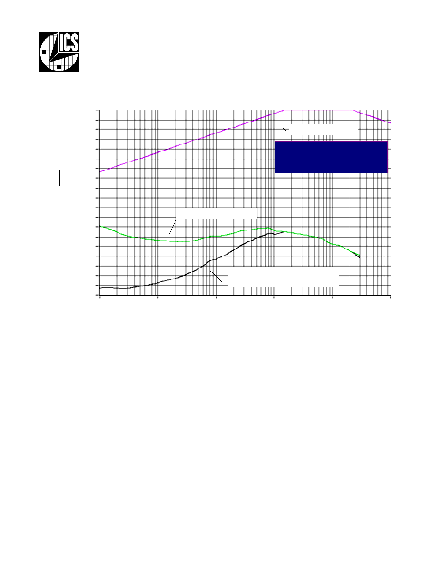
RMS Phase Jitter (Random)
1.5MHz to 22MHz = 2.42ps (typical)
O
FFSET
F
REQUENCY
(H
Z
)
N
OISE
P
O
WER
dBc
Hz
Phase Noise Result by adding
PCI ExpressTM Filter to raw data
PCI ExpressTM Filter
The illustrated phase noise plot was taken using a low phase
noise signal generator, the noise floor of the signal generator is
less than that of the device under test.
Using this configuration allows one to see the true spectral purity
or phase noise performance of the PLL in the device under test.
Due to the tracking ability of a PLL, it will track the input signal
up to its loop bandwidth. Therefore, if the input phase noise is
greater than that of the PLL, it will increase the output phase
noise performance of the device. It is recommended that the
phase noise performance of the input is verified in order to
achieve the above phase noise performance.
Raw Phase Noise Data

9DB202CG
www.icst.com/products/hiperclocks.html
REV. A OCTOBER 6, 2004
6
Integrated
Circuit
Systems, Inc.
ICS9DB202
PCI E
XPRESS
TM
J
ITTER
A
TTENUATOR
SCOPE
Qx
HCSL
P
ARAMETER
M
EASUREMENT
I
NFORMATION
O
UTPUT
S
KEW
D
IFFERENTIAL
I
NPUT
L
EVEL
3.3V HCSL O
UTPUT
L
OAD
AC T
EST
C
IRCUIT
0V
C
YCLE
-
TO
-C
YCLE
J
ITTER
O
UTPUT
D
UTY
C
YCLE
/P
ULSE
W
IDTH
/P
ERIOD
3.3V±5%
V
CMR
Cross Points
V
PP
GND
CLK
nCLK
V
DD
tsk(o)
PCIEXCx
Clock
Outputs
20%
80%
80%
20%
t
R
t
F
V
SW I N G
PCIEXTy
PCIEXCx
PCIEXTy
HCSL O
UTPUT
R
ISE
/F
ALL
T
IME
Pulse Width
t
PERIOD
t
PW
t
PERIOD
odc =
PCIEXT0,
PCIEXT1
PCIEXC0,
PCIEXC1
V
DD,
V
DDA
GND
PCIEXT0,
PCIEXT1
PCIEXC0,
PCIEXC1
t
jit(cc) =
t
cycle n ≠
t
cycle n+1
1000 Cycles
t
cycle n
t
cycle n+1

9DB202CG
www.icst.com/products/hiperclocks.html
REV. A OCTOBER 6, 2004
7
Integrated
Circuit
Systems, Inc.
ICS9DB202
PCI E
XPRESS
TM
J
ITTER
A
TTENUATOR
A
PPLICATION
I
NFORMATION
Figure 2 shows how the differential input can be wired to accept
single ended levels. The reference voltage V_REF = V
DD
/2 is
generated by the bias resistors R1, R2 and C1. This bias circuit
should be located as close as possible to the input pin. The ratio
F
IGURE
2. S
INGLE
E
NDED
S
IGNAL
D
RIVING
D
IFFERENTIAL
I
NPUT
W
IRING
THE
D
IFFERENTIAL
I
NPUT
TO
A
CCEPT
S
INGLE
E
NDED
L
EVELS
of R1 and R2 might need to be adjusted to position the V_REF in
the center of the input voltage swing. For example, if the input
clock swing is only 2.5V and V
DD
= 3.3V, V_REF should be 1.25V
and R2/R1 = 0.609.
V_REF
R1
1K
C1
0.1u
R2
1K
Single Ended Clock Input
CLK
nCLK
VDD
P
OWER
S
UPPLY
F
ILTERING
T
ECHNIQUES
As in any high speed analog circuitry, the power supply pins are
vulnerable to random noise. The ICS9DB202 provides separate
power supplies to isolate any high switching noise from the out-
puts to the internal PLL. V
DD
and V
DDA
should be individually con-
nected to the power supply plane through vias, and bypass ca-
pacitors should be used for each pin. To achieve optimum jitter
performance, power supply isolation is required.
Figure 1 illus-
trates how a 24
resistor along with a 10µF and a .01µF by-
pass capacitor should be connected to each V
DDA
pin.
F
IGURE
1. P
OWER
S
UPPLY
F
ILTERING
24
V
DDA
10
µF
.01
µF
3.3V
.01
µF
V
DD

9DB202CG
www.icst.com/products/hiperclocks.html
REV. A OCTOBER 6, 2004
8
Integrated
Circuit
Systems, Inc.
ICS9DB202
PCI E
XPRESS
TM
J
ITTER
A
TTENUATOR
F
IGURE
3C. H
I
P
ER
C
LOCK
S CLK/
N
CLK I
NPUT
D
RIVEN
BY
3.3V LVPECL D
RIVER
F
IGURE
3B. H
I
P
ER
C
LOCK
S CLK/
N
CLK I
NPUT
D
RIVEN
BY
3.3V LVPECL D
RIVER
F
IGURE
3D. H
I
P
ER
C
LOCK
S CLK/
N
CLK I
NPUT
D
RIVEN
BY
3.3V LVDS D
RIVER
3.3V
R1
50
R3
50
Zo = 50 Ohm
LVPECL
Zo = 50 Ohm
HiPerClockS
CLK
nCLK
3.3V
Input
R2
50
Zo = 50 Ohm
Input
HiPerClockS
CLK
nCLK
3.3V
R3
125
R2
84
Zo = 50 Ohm
3.3V
R4
125
LVPECL
R1
84
3.3V
D
IFFERENTIAL
C
LOCK
I
NPUT
I
NTERFACE
The CLK /nCLK accepts LVDS, LVPECL, LVHSTL, SSTL, HCSL
and other differential signals. Both V
SWING
and V
OH
must meet the
V
PP
and V
CMR
input requirements. Figures 3A to 3D show inter-
face examples for the HiPerClockS CLK/nCLK input driven by
the most common driver types. The input interfaces suggested
F
IGURE
3A. H
I
P
ER
C
LOCK
S CLK/
N
CLK I
NPUT
D
RIVEN
BY
ICS H
I
P
ER
C
LOCK
S LVHSTL D
RIVER
here are examples only. Please consult with the vendor of the
driver component to confirm the driver termination requirements.
For example in
Figure 3A, the input termination applies for ICS
HiPerClockS LVHSTL drivers. If you are using an LVHSTL driver
from another vendor, use their termination recommendation.
1.8V
R2
50
Input
LVHSTL Driver
ICS
HiPerClockS
R1
50
LVHSTL
3.3V
Zo = 50 Ohm
Zo = 50 Ohm
HiPerClockS
CLK
nCLK
Zo = 50 Ohm
R1
100
3.3V
LVDS_Driv er
Zo = 50 Ohm
Receiv er
CLK
nCLK
3.3V

9DB202CG
www.icst.com/products/hiperclocks.html
REV. A OCTOBER 6, 2004
9
Integrated
Circuit
Systems, Inc.
ICS9DB202
PCI E
XPRESS
TM
J
ITTER
A
TTENUATOR
R
ELIABILITY
I
NFORMATION
T
RANSISTOR
C
OUNT
The transistor count for ICS9DB202 is: 2471
T
ABLE
6A.
JA
VS
. A
IR
F
LOW
T
ABLE
F
OR
20 L
EAD
TSSOP P
ACKAGE
JA
by Velocity (Linear Feet per Minute)
0
200
500
Single-Layer PCB, JEDEC Standard Test Boards
114.5∞C/W
98∞C/W
88∞C/W
Multi-Layer PCB, JEDEC Standard Test Boards
73.2∞C/W
66.6∞C/W
63.5∞C/W
NOTE: Most modern PCB designs use multi-layered boards. The data in the second row pertains to most designs.
T
ABLE
6B.
JA
VS
. A
IR
F
LOW
T
ABLE
F
OR
20 L
EAD
SSOP P
ACKAGE
JA
by Velocity (Linear Feet per Minute)
0
200
500
Multi-Layer PCB, JEDEC Standard Test Boards
80.8∞C/W
73.2∞C/W
69.2∞C/W
NOTE: Most modern PCB designs use multi-layered boards. The data in the second row pertains to most designs.

9DB202CG
www.icst.com/products/hiperclocks.html
REV. A OCTOBER 6, 2004
10
Integrated
Circuit
Systems, Inc.
ICS9DB202
PCI E
XPRESS
TM
J
ITTER
A
TTENUATOR
P
ACKAGE
O
UTLINE
- F S
UFFIX
FOR
20 L
EAD
SSOP
T
ABLE
6B. P
ACKAGE
D
IMENSIONS
Reference Document: JEDEC Publication 95, MO-150
P
ACKAGE
O
UTLINE
- G S
UFFIX
FOR
20 L
EAD
TSSOP
T
ABLE
6A. P
ACKAGE
D
IMENSIONS
Reference Document: JEDEC Publication 95, MO-153
L
O
B
M
Y
S
s
r
e
t
e
m
i
l
l
i
M
m
u
m
i
n
i
M
m
u
m
i
x
a
M
N
0
2
A
-
-
0
2
.
1
1
A
5
0
.
0
5
1
.
0
2
A
0
8
.
0
5
0
.
1
b
9
1
.
0
0
3
.
0
c
9
0
.
0
0
2
.
0
D
0
4
.
6
0
6
.
6
E
C
I
S
A
B
0
4
.
6
1
E
0
3
.
4
0
5
.
4
e
C
I
S
A
B
5
6
.
0
L
5
4
.
0
5
7
.
0
∞
0
∞
8
a
a
a
-
-
0
1
.
0
L
O
B
M
Y
S
s
r
e
t
e
m
i
l
l
i
M
m
u
m
i
n
i
M
m
u
m
i
x
a
M
N
0
2
A
-
-
0
.
2
1
A
5
0
.
0
-
-
2
A
5
6
.
1
5
8
.
1
b
2
2
.
0
8
3
.
0
c
9
0
.
0
5
2
.
0
D
0
9
.
6
0
5
.
7
E
0
4
.
7
0
2
.
8
1
E
0
.
5
0
6
.
5
e
C
I
S
A
B
5
6
.
0
L
5
5
.
0
5
9
.
0
∞
0
∞
8

9DB202CG
www.icst.com/products/hiperclocks.html
REV. A OCTOBER 6, 2004
11
Integrated
Circuit
Systems, Inc.
ICS9DB202
PCI E
XPRESS
TM
J
ITTER
A
TTENUATOR
T
ABLE
7. O
RDERING
I
NFORMATION
While the information presented herein has been checked for both accuracy and reliability, Integrated Circuit Systems, Incorporated (ICS) assumes no responsibility for either its use
or for infringement of any patents or other rights of third parties, which would result from its use. No other circuits, patents, or licenses are implied. This product is intended for use
in normal commercial applications. Any other applications such as those requiring extended temperature range, high reliability, or other extraordinary environmental requirements are
not recommended without additional processing by ICS. ICS reserves the right to change any circuitry or specifications without notice. ICS does not authorize or warrant any ICS
product for use in life support devices or critical medical instruments.
r
e
b
m
u
N
r
e
d
r
O
/
t
r
a
P
g
n
i
k
r
a
M
e
g
a
k
c
a
P
t
n
u
o
C
e
r
u
t
a
r
e
p
m
e
T
G
C
2
0
2
B
D
9
S
C
I
G
C
2
0
2
B
D
9
S
C
I
P
O
S
S
T
d
a
e
L
0
2
e
b
u
T
r
e
p
2
7
C
∞
0
7
o
t
C
∞
0
T
G
C
2
0
2
B
D
9
S
C
I
G
C
2
0
2
B
D
9
S
C
I
l
e
e
R
d
n
a
e
p
a
T
n
o
P
O
S
S
T
d
a
e
L
0
2
0
0
5
2
C
∞
0
7
o
t
C
∞
0
F
L
G
C
2
0
2
B
D
9
S
C
I
L
G
C
2
0
2
B
D
9
S
C
I
P
O
S
S
T
"
e
e
r
F
-
d
a
e
L
"
d
a
e
L
0
2
e
b
u
T
r
e
p
2
7
C
∞
0
7
o
t
C
∞
0
T
F
L
G
C
2
0
2
B
D
9
S
C
I
L
G
C
2
0
2
B
D
9
S
C
I
n
o
P
O
S
S
T
"
e
e
r
F
-
d
a
e
L
"
d
a
e
L
0
2
l
e
e
R
d
n
a
e
p
a
T
0
0
5
2
C
∞
0
7
o
t
C
∞
0
F
C
2
0
2
B
D
9
S
C
I
F
C
2
0
2
B
D
9
S
C
I
P
O
S
S
d
a
e
L
0
2
e
b
u
T
r
e
p
4
6
C
∞
0
7
o
t
C
∞
0
T
F
C
2
0
2
B
D
9
S
C
I
F
C
2
0
2
B
D
9
S
C
I
l
e
e
R
d
n
a
e
p
a
T
n
o
P
O
S
S
d
a
e
L
0
2
0
0
0
1
C
∞
0
7
o
t
C
∞
0
F
L
F
C
2
0
2
B
D
9
S
C
I
F
L
F
C
2
0
2
B
D
9
S
C
I
P
O
S
S
"
e
e
r
F
-
d
a
e
L
"
d
a
e
L
0
2
e
b
u
T
r
e
p
4
6
C
∞
0
7
o
t
C
∞
0
T
F
L
F
C
2
0
2
B
D
9
S
C
I
F
L
F
C
2
0
2
B
D
9
S
C
I
n
o
P
O
S
S
"
e
e
r
F
-
d
a
e
L
"
d
a
e
L
0
2
l
e
e
R
d
n
a
e
p
a
T
0
0
0
1
C
∞
0
7
o
t
C
∞
0
The aforementioned trademarks, HiPerClockSTM and PCI ExpressTM iare trademarks of Integrated Circuit Systems, Inc. or its subsidiaries in the United States and/or other countries.