DATASHEET SEARCH SITE | WWW.ALLDATASHEET.COM
9DB306BL
www.icst.com/products/hiperclocks.html
REV. A APRIL 7, 2005
1
Integrated
Circuit
Systems, Inc.
ICS9DB306
PCI E
XPRESS
,
J
ITTER
A
TTENUATOR
G
ENERAL
D
ESCRIPTION
The ICS9DB306 is a high performance 1-to-6
Differential-to LVPECL Jitter Attenuator designed
for use in PCI ExpressTM systems. In some PCI
ExpressTM systems, such as those found in desktop
PCs, the PCI ExpressTM clocks are generated from
a low bandwidth, high phase noise PLL frequency
synthesizer. In these systems, a zero delay buffer may be
required to attenuate high frequency random and deterministic
jitter components from the PLL synthesizer and from the system
board. The ICS9DB306 has 2 PLL bandwidth modes. In low
bandwidth mode, the PLL loop BW is about 500kHz and this
setting will attenuate much of the jitter from the reference clock
input while being high enough to pass a triangular input spread
spectrum profile. There is also a high bandwidth mode which
sets the PLL bandwidth at 1MHz which will pass more spread
spectrum modulation.
For serdes which have x30 reference multipliers instead of x25
multipliers, 5 of the 6 PCI ExpressTM outputs (PCIEX1:5) can be
set for 125MHz instead of 100MHz by configuring the appropri-
ate frequency select pins (FS0:1). Output PCIEX0 will always
run at the reference clock frequency (usually 100MHz) in desk-
top PC PCI ExpressTM Applications.
Features
� Six differential LVPECL output pairs
� 1 differential clock input
� CLK and nCLK supports the following input types:
LVPECL, LVDS, LVHSTL, SSTL, HCSL
� Maximum output frequency: 140MHz
� Output skew: 135ps (maximum)
� Cycle-to-Cycle jitter: 25ps (maximum)
� RMS phase jitter @ 100MHz, (1.5MHz - 22MHz):
3ps (typical)
� 3.3V operating supply
� 0�C to 70�C ambient operating temperature
� Lead-Free package fully RoHS compliant
� Industrial temperature information available upon request
HiPerClockSTM
ICS
P
IN
A
SSIGNMENT
nOE0
CLK
nCLK
BYPASS
nOE1
PCIEXT0
nPCIEXC0
PCIEXT1
nPCIEXC1
PCIEXT2
nPCIEXC2
PCIEXT3
nPCIEXC3
PCIEXT4
nPCIEXC4
PCIEXT5
nPCIEXC5
B
LOCK
D
IAGRAM
ICS9DB306
28-Lead TSSOP, 173-MIL
4.4mm x 9.7mm x 0.92mm
body package
L Package
Top View
V
EE
PCIEXT1
PCIEXC1
PCIEXT2
PCIEXC2
V
CC
nOE0
nOE1
V
CC
PCIEXC3
PCIEXT3
PCIEXC4
PCIEXT4
V
EE
V
CC
PCIEXC0
PCIEXT0
FS0
nCLK
CLK
PLL_BW
V
CCA
V
EE
BYPASS
FS1
PCIEXT5
PCIEXC5
V
CC
ICS9DB306
28-Lead, 209-MIL SSOP
5.3mm x 10.2mm x 1.75mm
body package
F Package
Top View
Phase
Detector
VCO
Loop
Filter
1 Disabled
0 Enabled
1 Disabled
0 Enabled
�5
0 �4
1 �5
0 �5
1 �4
FS0
FS1
Internal Feedback
�5
0
1
0
1
0
1
Buffer
1
2
3
4
5
6
7
8
9
10
11
12
13
14
28
27
26
25
24
23
22
21
20
19
18
17
16
15
9DB306BL
www.icst.com/products/hiperclocks.html
REV. A APRIL 7, 2005
2
Integrated
Circuit
Systems, Inc.
ICS9DB306
PCI E
XPRESS
,
J
ITTER
A
TTENUATOR
T
ABLE
2. P
IN
C
HARACTERISTICS
T
ABLE
3A. R
ATIO
OF
O
UTPUT
F
REQUENCY
TO
I
NPUT
F
REQUENCY
F
UNCTION
T
ABLE
, FS0
l
o
b
m
y
S
r
e
t
e
m
a
r
a
P
s
n
o
i
t
i
d
n
o
C
t
s
e
T
m
u
m
i
n
i
M
l
a
c
i
p
y
T
m
u
m
i
x
a
M
s
t
i
n
U
C
N
I
e
c
n
a
t
i
c
a
p
a
C
t
u
p
n
I
4
F
p
R
P
U
L
L
U
P
r
o
t
s
i
s
e
R
p
u
ll
u
P
t
u
p
n
I
1
5
K
R
N
W
O
D
L
L
U
P
r
o
t
s
i
s
e
R
n
w
o
d
ll
u
P
t
u
p
n
I
1
5
K
s
t
u
p
n
I
s
t
u
p
t
u
O
0
S
F
0
X
E
I
C
P
1
X
E
I
C
P
2
X
E
I
C
P
0
1
4
/
5
4
/
5
1
1
1
1
T
ABLE
3C. O
UTPUT
E
NABLE
F
UNCTION
T
ABLE
, nOE0
T
ABLE
1. P
IN
D
ESCRIPTIONS
r
e
b
m
u
N
e
m
a
N
e
p
y
T
n
o
i
t
p
i
r
c
s
e
D
0
2
,
4
1
,
1
V
E
E
r
e
w
o
P
.
s
n
i
p
y
l
p
p
u
s
e
v
i
t
a
g
e
N
3
,
2
,
1
T
X
E
I
C
P
1
C
X
E
I
C
P
t
u
p
t
u
O
.
s
l
e
v
e
l
e
c
a
f
r
e
t
n
i
L
C
E
P
V
L
.
s
r
i
a
p
t
u
p
t
u
o
l
a
i
t
n
e
r
e
f
f
i
D
5
,
4
,
2
T
X
E
I
C
P
2
C
X
E
I
C
P
t
u
p
t
u
O
.
s
l
e
v
e
l
e
c
a
f
r
e
t
n
i
L
C
E
P
V
L
.
s
r
i
a
p
t
u
p
t
u
o
l
a
i
t
n
e
r
e
f
f
i
D
8
2
,
5
1
,
9
,
6
V
C
C
r
e
w
o
P
.
s
n
i
p
y
l
p
p
u
s
e
r
o
C
8
,
7
1
E
O
n
,
0
E
O
n
t
u
p
n
I
n
w
o
d
ll
u
P
o
g
o
t
)
x
T
X
E
I
C
P
(
s
t
u
p
t
u
o
e
u
r
t
s
e
c
r
o
f
,
H
G
I
H
n
e
h
W
.
e
l
b
a
n
e
t
u
p
t
u
O
,
W
O
L
n
e
h
W
.
H
G
I
H
o
g
o
t
)
x
C
X
E
I
C
P
(
s
t
u
p
t
u
o
d
e
t
r
e
v
n
i
e
h
t
d
n
a
W
O
L
.
s
l
e
v
e
l
e
c
a
f
r
e
t
n
i
L
T
T
V
L
/
S
O
M
C
V
L
.
d
e
l
b
a
n
e
e
r
a
s
t
u
p
t
u
o
1
1
,
0
1
,
3
C
X
E
I
C
P
3
T
X
E
I
C
P
t
u
p
t
u
O
.
s
l
e
v
e
l
e
c
a
f
r
e
t
n
i
L
C
E
P
V
L
.
s
r
i
a
p
t
u
p
t
u
o
l
a
i
t
n
e
r
e
f
f
i
D
3
1
,
2
1
,
4
C
X
E
I
C
P
4
T
X
E
I
C
P
t
u
p
t
u
O
.
s
l
e
v
e
l
e
c
a
f
r
e
t
n
i
L
C
E
P
V
L
.
s
r
i
a
p
t
u
p
t
u
o
l
a
i
t
n
e
r
e
f
f
i
D
7
1
,
6
1
,
5
C
X
E
I
C
P
5
T
X
E
I
C
P
t
u
p
t
u
O
.
s
l
e
v
e
l
e
c
a
f
r
e
t
n
i
L
C
E
P
V
L
.
s
r
i
a
p
t
u
p
t
u
o
l
a
i
t
n
e
r
e
f
f
i
D
8
1
1
S
F
n
w
o
d
ll
u
P
.
s
l
e
v
e
l
e
c
a
f
r
e
t
n
i
L
T
T
V
L
/
S
O
M
C
V
L
.
n
i
p
t
c
e
l
e
s
y
c
n
e
u
q
e
r
F
9
1
S
S
A
P
Y
B
t
u
p
n
I
n
w
o
d
ll
u
P
e
h
t
d
n
a
,
e
d
o
m
s
s
a
p
y
b
n
i
s
i
L
L
P
e
h
t
,
H
G
I
H
n
e
h
W
.
n
i
p
t
c
e
l
e
s
s
s
a
p
y
B
.
s
l
e
v
e
l
e
c
a
f
r
e
t
n
i
L
T
T
V
L
/
S
O
M
C
V
L
.
r
e
f
f
u
b
6
:
1
a
s
a
n
o
i
t
c
n
u
f
n
a
c
e
c
i
v
e
d
1
2
V
A
C
C
r
e
w
o
P
4
2
s
e
r
i
u
q
e
R
.
n
i
p
y
l
p
p
u
s
g
o
l
a
n
A
.
r
o
t
s
i
s
e
r
s
e
i
r
e
s
2
2
W
B
_
L
L
P
t
u
p
n
I
p
u
ll
u
P
.
s
l
e
v
e
l
e
c
a
f
r
e
t
n
i
L
T
T
V
L
/
S
O
M
C
V
L
.
t
u
p
n
i
h
t
d
i
w
d
n
a
B
L
L
P
s
t
c
e
l
e
S
3
2
K
L
C
t
u
p
n
I
n
w
o
d
ll
u
P
.
t
u
p
n
i
k
c
o
l
c
l
a
i
t
n
e
r
e
f
f
i
d
g
n
i
t
r
e
v
n
i
-
n
o
N
4
2
K
L
C
n
t
u
p
n
I
/
p
u
ll
u
P
n
w
o
d
ll
u
P
V
.
t
u
p
n
i
k
c
o
l
c
l
a
i
t
n
e
r
e
f
f
i
d
g
n
i
t
r
e
v
n
I
C
C
.
g
n
i
t
a
o
l
f
t
f
e
l
n
e
h
w
t
l
u
a
f
e
d
2
/
5
2
0
S
F
t
u
p
n
I
p
u
ll
u
P
.
s
l
e
v
e
l
e
c
a
f
r
e
t
n
i
L
T
T
V
L
/
S
O
M
C
V
L
.
n
i
p
t
c
e
l
e
s
y
c
n
e
u
q
e
r
F
7
2
,
6
2
,
0
T
X
E
I
C
P
0
C
X
E
I
C
P
t
u
p
t
u
O
.
s
l
e
v
e
l
e
c
a
f
r
e
t
n
i
L
C
E
P
V
L
.
s
r
i
a
p
t
u
p
t
u
o
l
a
i
t
n
e
r
e
f
f
i
D
:
E
T
O
N
p
u
ll
u
P
d
n
a
n
w
o
d
ll
u
P
.
s
e
u
l
a
v
l
a
c
i
p
y
t
r
o
f
,
s
c
i
t
s
i
r
e
t
c
a
r
a
h
C
n
i
P
,
2
e
l
b
a
T
e
e
S
.
s
r
o
t
s
i
s
e
r
t
u
p
n
i
l
a
n
r
e
t
n
i
o
t
r
e
f
e
r
T
ABLE
3B. R
ATIO
OF
O
UTPUT
F
REQUENCY
TO
I
NPUT
F
REQUENCY
F
UNCTION
T
ABLE
, FS1
s
t
u
p
n
I
s
t
u
p
t
u
O
1
S
F
3
X
E
I
C
P
4
X
E
I
C
P
5
X
E
I
C
P
0
1
1
1
1
4
/
5
4
/
5
4
/
5
s
t
u
p
n
I
s
t
u
p
t
u
O
0
E
O
n
2
:
0
X
E
I
C
P
0
d
e
l
b
a
n
E
1
d
e
l
b
a
s
i
D
T
ABLE
3D. O
UTPUT
E
NABLE
F
UNCTION
T
ABLE
, nOE1
s
t
u
p
n
I
s
t
u
p
t
u
O
1
E
O
n
5
:
3
X
E
I
C
P
0
d
e
l
b
a
n
E
1
d
e
l
b
a
s
i
D
T
ABLE
3E. PLL B
ANDWIDTH
F
UNCTION
T
ABLE
s
t
u
p
n
I
h
t
d
i
w
d
n
a
B
W
B
_
L
L
P
0
z
H
k
0
0
5
1
z
H
M
1
T
ABLE
3F. PLL M
ODE
F
UNCTION
T
ABLE
s
t
u
p
n
I
e
d
o
M
L
L
P
S
S
A
P
Y
B
1
d
e
l
b
a
s
i
D
0
d
e
l
b
a
n
E
9DB306BL
www.icst.com/products/hiperclocks.html
REV. A APRIL 7, 2005
3
Integrated
Circuit
Systems, Inc.
ICS9DB306
PCI E
XPRESS
,
J
ITTER
A
TTENUATOR
T
ABLE
4C. D
IFFERENTIAL
DC C
HARACTERISTICS
,
V
CC
= 3.3V�5%, T
A
= 0�C
TO
70�C
l
o
b
m
y
S
r
e
t
e
m
a
r
a
P
s
n
o
i
t
i
d
n
o
C
t
s
e
T
m
u
m
i
n
i
M
l
a
c
i
p
y
T
m
u
m
i
x
a
M
s
t
i
n
U
I
H
I
t
n
e
r
r
u
C
h
g
i
H
t
u
p
n
I
K
L
C
n
,
K
L
C
V
C
C
V
=
N
I
V
5
6
4
.
3
=
0
5
1
A
�
I
L
I
t
n
e
r
r
u
C
w
o
L
t
u
p
n
I
K
L
C
n
,
K
L
C
V
C
C
V
,
V
5
6
4
.
3
=
N
I
V
0
=
0
5
1
A
�
V
P
P
e
g
a
t
l
o
V
t
u
p
n
I
k
a
e
P
-
o
t
-
k
a
e
P
5
1
.
0
3
.
1
V
V
R
M
C
2
,
1
E
T
O
N
;
e
g
a
t
l
o
V
t
u
p
n
I
e
d
o
M
n
o
m
m
o
C
V
E
E
5
.
0
+
V
C
C
5
8
.
0
-
V
V
s
a
d
e
n
i
f
e
d
s
i
e
g
a
t
l
o
v
e
d
o
m
n
o
m
m
o
C
:
1
E
T
O
N
H
I
.
V
s
i
K
L
C
n
,
K
L
C
r
o
f
e
g
a
t
l
o
v
t
u
p
n
i
m
u
m
i
x
a
m
e
h
t
,
s
n
o
i
t
a
c
il
p
p
a
d
e
d
n
e
e
l
g
n
i
s
r
o
F
:
2
E
T
O
N
C
C
.
V
3
.
0
+
T
ABLE
4A. P
OWER
S
UPPLY
DC C
HARACTERISTICS
,
V
CC
= 3.3V�5%, T
A
= 0�C
TO
70�C
T
ABLE
4B. LVCMOS / LVTTL DC C
HARACTERISTICS
,
V
CC
= 3.3V�5%, T
A
= 0�C
TO
70�C
l
o
b
m
y
S
r
e
t
e
m
a
r
a
P
s
n
o
i
t
i
d
n
o
C
t
s
e
T
m
u
m
i
n
i
M
l
a
c
i
p
y
T
m
u
m
i
x
a
M
s
t
i
n
U
V
C
C
e
g
a
t
l
o
V
y
l
p
p
u
S
e
r
o
C
5
3
1
.
3
3
.
3
5
6
4
.
3
V
V
A
C
C
e
g
a
t
l
o
V
y
l
p
p
u
S
g
o
l
a
n
A
5
3
1
.
3
3
.
3
5
6
4
.
3
V
I
C
C
t
n
e
r
r
u
C
y
l
p
p
u
S
r
e
w
o
P
5
3
1
A
m
I
A
C
C
t
n
e
r
r
u
C
y
l
p
p
u
S
g
o
l
a
n
A
5
2
A
m
l
o
b
m
y
S
r
e
t
e
m
a
r
a
P
s
n
o
i
t
i
d
n
o
C
t
s
e
T
m
u
m
i
n
i
M
l
a
c
i
p
y
T
m
u
m
i
x
a
M
s
t
i
n
U
V
H
I
e
g
a
t
l
o
V
h
g
i
H
t
u
p
n
I
2
V
C
C
3
.
0
+
V
m
V
L
I
e
g
a
t
l
o
V
w
o
L
t
u
p
n
I
3
.
0
-
8
.
0
V
m
I
H
I
t
n
e
r
r
u
C
h
g
i
H
t
u
p
n
I
,
1
S
F
,
1
E
O
n
,
0
E
O
n
S
S
A
P
Y
B
V
C
C
V
=
N
I
V
5
6
4
.
3
=
0
5
1
A
�
W
B
_
L
L
P
,
0
S
F
5
A
�
I
L
I
t
n
e
r
r
u
C
w
o
L
t
u
p
n
I
,
1
S
F
,
1
E
O
n
,
0
E
O
n
S
S
A
P
Y
B
V
C
C
V
,
V
5
6
4
.
3
=
N
I
V
0
=
5
-
A
�
W
B
_
L
L
P
,
0
S
F
0
5
1
-
A
�
A
BSOLUTE
M
AXIMUM
R
ATINGS
Supply Voltage, V
CC
4.6V
Inputs, V
I
-0.5V to V
CC
+ 0.5V
Outputs, I
O
Continuous Current
50mA
Surge Current
100mA
Package Thermal Impedance,
JA
49.8�C/W (0 lfpm)
Storage Temperature, T
STG
-65�C to 150�C
NOTE: Stresses beyond those listed under Absolute
Maximum Ratings may cause permanent damage to the
device. These ratings are stress specifications only. Functional
operation of product at these conditions or any conditions be-
yond those listed in the
DC Characteristics or AC Character-
istics is not implied. Exposure to absolute maximum rating
conditions for extended periods may affect product reliability.
9DB306BL
www.icst.com/products/hiperclocks.html
REV. A APRIL 7, 2005
4
Integrated
Circuit
Systems, Inc.
ICS9DB306
PCI E
XPRESS
,
J
ITTER
A
TTENUATOR
T
ABLE
5. AC C
HARACTERISTICS
,
V
CC
= 3.3V�5%, T
A
= 0�C
TO
70�C
l
o
b
m
y
S
r
e
t
e
m
a
r
a
P
s
n
o
i
t
i
d
n
o
C
t
s
e
T
m
u
m
i
n
i
M
l
a
c
i
p
y
T
m
u
m
i
x
a
M
s
t
i
n
U
f
X
A
M
y
c
n
e
u
q
e
r
F
t
u
p
t
u
O
0
4
1
z
H
M
t
)
o
(
k
s
2
,
1
E
T
O
N
;
w
e
k
S
t
u
p
t
u
O
5
5
5
3
1
s
p
t
)
c
c
(
t
ij
2
E
T
O
N
,
r
e
t
t
i
J
e
l
c
y
C
-
o
t
-
e
l
c
y
C
5
2
s
p
t
)
�
(
t
ij
;
)
m
o
d
n
a
R
(
r
e
t
t
i
J
e
s
a
h
P
S
M
R
3
E
T
O
N
:
e
g
n
a
R
n
o
i
t
a
r
g
e
t
n
I
z
H
M
2
2
-
z
H
M
5
.
1
3
s
p
t
R
t
/
F
e
m
i
T
ll
a
F
/
e
s
i
R
t
u
p
t
u
O
%
0
8
o
t
%
0
2
0
0
2
0
0
7
s
p
c
d
o
e
l
c
y
C
y
t
u
D
t
u
p
t
u
O
8
4
2
5
%
.
s
n
o
i
t
i
d
n
o
c
d
a
o
l
l
a
u
q
e
h
t
i
w
d
n
a
e
g
a
t
l
o
v
y
l
p
p
u
s
e
m
a
s
e
h
t
t
a
s
t
u
p
t
u
o
n
e
e
w
t
e
b
w
e
k
s
s
a
d
e
n
i
f
e
D
:
1
E
T
O
N
.
s
t
n
i
o
p
s
s
o
r
c
l
a
i
t
n
e
r
e
f
f
i
d
t
u
p
t
u
o
e
h
t
t
a
d
e
r
u
s
a
e
M
.
5
6
d
r
a
d
n
a
t
S
C
E
D
E
J
h
t
i
w
e
c
n
a
d
r
o
c
c
a
n
i
d
e
n
i
f
e
d
s
i
r
e
t
e
m
a
r
a
p
s
i
h
T
:
2
E
T
O
N
.
n
o
i
t
c
e
s
s
i
h
t
g
n
i
w
o
ll
o
f
t
o
l
P
e
s
i
o
N
e
s
a
h
P
e
h
t
o
t
r
e
f
e
r
e
s
a
e
l
P
:
3
E
T
O
N
T
ABLE
4D. LVPECL DC C
HARACTERISTICS
,
V
CC
= 3.3V�5%, T
A
= 0�C
TO
70�C
l
o
b
m
y
S
r
e
t
e
m
a
r
a
P
s
n
o
i
t
i
d
n
o
C
t
s
e
T
m
u
m
i
n
i
M
l
a
c
i
p
y
T
m
u
m
i
x
a
M
s
t
i
n
U
V
H
O
1
E
T
O
N
;
e
g
a
t
l
o
V
h
g
i
H
t
u
p
t
u
O
V
C
C
4
.
1
-
V
C
C
9
.
0
-
V
V
L
O
1
E
T
O
N
;
e
g
a
t
l
o
V
w
o
L
t
u
p
t
u
O
V
C
C
0
.
2
-
V
C
C
7
.
1
-
V
V
G
N
I
W
S
g
n
i
w
S
e
g
a
t
l
o
V
t
u
p
t
u
O
k
a
e
P
-
o
t
-
k
a
e
P
6
.
0
0
.
1
V
0
5
h
t
i
w
d
e
t
a
n
i
m
r
e
t
s
t
u
p
t
u
O
:
1
E
T
O
N
V
o
t
C
C
.
V
2
-
9DB306BL
www.icst.com/products/hiperclocks.html
REV. A APRIL 7, 2005
5
Integrated
Circuit
Systems, Inc.
ICS9DB306
PCI E
XPRESS
,
J
ITTER
A
TTENUATOR
T
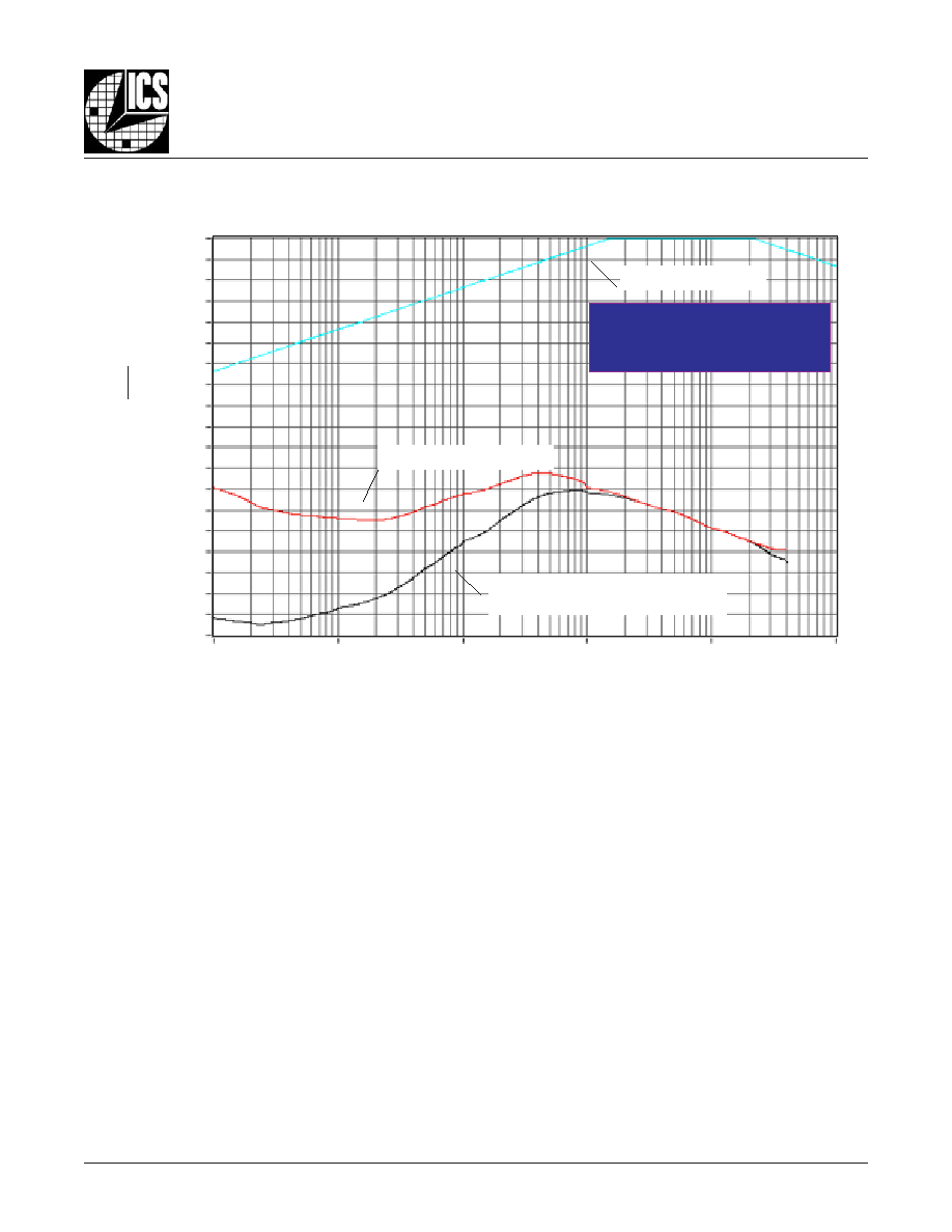
YPICAL
P
HASE
N
OISE
AT
100MH
Z
0
-10
-20
-30
-40
-50
-60
-70
-80
-90
-100
-110
-120
-130
-140
-150
-160
-170
-180
-190
1k
10k
100k
1M
10M
100M
100MHz
RMS Phase Jitter (Random)
1.5MHz to 22MHz = 3ps (typical)
O
FFSET
F
REQUENCY
(H
Z
)
N
OISE
P
O
WER
dBc
Hz
Phase Noise Result by adding
PCI ExpressTM Filter to raw data
PCI ExpressTM Filter
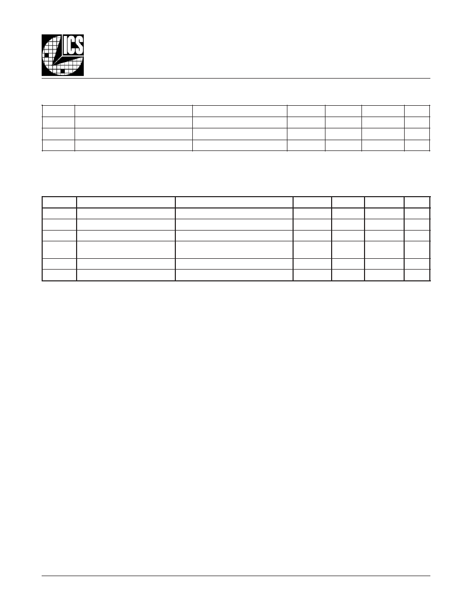
The illustrated phase noise plot was taken using a low phase
noise signal generator, the noise floor of the signal generator is
less than that of the device under test.
Using this configuration allows one to see the true spectral pu-
rity or phase noise performance of the PLL in the device under
test. Due to the tracking ability of a PLL, it will track the input
signal up to its loop bandwidth. Therefore, if the input phase noise
is greater than that of the VCO, it will increase the output phase
noise performance of the device. It is recommended that the
phase noise performance of the input is verified in order to
achieve the above phase noise performance.
Raw Phase Noise Data
Document Outline
- General Description
- Features
- Block Diagram
- Pin Assignments
- Pin Descriptions
- Pin Characteristics
- Ratio of Output Frequency to Input Frequency Function Table, FS0
- Ratio of Output Frequency to Input Frequency Function Table, FS1
- Output Enable Function Table, nOE0
- Output Enable Function Table, nOE1
- PLL Bandwith Table
- PLL Mode Function Table
- Absolute Maximum Ratings
- Power Supply DC Characteristics
- LVCMOS DC Characteristics
- Differential DC Characteristics
- LVPECL DC Characteristics
- AC Characteristics
- Typical Phase Noise Plot
- Parameter Measurement Information
- 3.3V Output Load AC Test Circuit Diagram
- Differential Input Level Diagram
- Output Skew Diagram
- Cycle-to-Cycle Jitter Diagram
- Output Rise/Fall Time Diagram
- Output Duty/Pulse Width/Period Diagram
- Application Information
- Power Supply Filtering Techniques
- Wiring the Differential Input to Accwept Single Ended Levels
- Termination for LVPECL Outputs
- Differential Clock Input Interface
- Schematic Example
- Power Considerations
- Power Dissipation
- Junction Temperature
- Thermal Resistance
- Calculations & Equations
- LVPECL Driver Circuit & Termination
- Reliability Information
- Transistor Count
- Package Outline for 28 Lead TSSOP
- Package Dimensions for 28 Lead TSSOP
- Package Outline for 28 Lead SSOP
- Package Dimensions for 28 Lead SSOP
- Ordering Information
- Revision History Sheet