
Integrated
Circuit
Systems, Inc.
ICS9FG104
0839D--06/02/05
Pin Configuration
Recommended Application:
Frequency Timing Generator for Differential CPU & SATA clocks
Features:
∑
Generates common CPU frequencies from 14.318 MHz
or 25 MHz
∑
Crystal or reference input
∑
4 - 0.7V current-mode differential output pairs
∑
Supports Serial-ATA at 100 MHz
∑
Two spread spectrum modes: 0 to -0.5 downspread and
+/-0.25% centerspread
∑
Unused inputs may be disabled in either driven or Hi-Z
state for power management.
∑
M/N Programming
Key Specifications:
∑
Output cycle-to-cycle jitter < 50 ps
∑
Output to output skew < 35 ps
∑
+/-300 ppm frequency accuracy on output clocks
Programmable FTG for Differential P4
TM
CPU, PCI-Express & SATA Clocks
28-pin SSOP/TSSOP
Frequency Select Table
SEL14M_25M#
(FS3)
FS2 FS1 FS0 OUTPUT(MHz)
0
0
0
0
100.00
0
0
0
1
125.00
0
0
1
0
133.33
0
0
1
1
166.67
0
1
0
0
200.00
0
1
0
1
266.00
0
1
1
0
333.00
0
1
1
1
400.00
1
0
0
0
100.00
1
0
0
1
125.00
1
0
1
0
133.33
1
0
1
1
166.67
1
1
0
0
200.00
1
1
0
1
266.00
1
1
1
0
333.00
1
1
1
1
400.00
XIN/CLKIN
1
28 VDDA
X2
2
27 GNDA
VDD
3
26 IREF
GND
4
25 FS0
REFOUT
5
24 FS1
FS2
6
23 DIF_0
DIF_3
7
22 DIF_0#
DIF_3#
8
21 VDD
VDD
9
20 GND
GND 10
19 DIF_1
DIF_2 11
18 DIF_1#
DIF_2# 12
17 SEL14M_25M#
SDATA 13
16 SPREAD
SCLK 14
15 DIF_STOP#
IC
S9
F
G
104

2
Integrated
Circuit
Systems, Inc.
ICS9FG104
0839D--06/02/05
Pin Description
PIN #
PIN NAME
PIN TYPE
DESCRIPTION
1
XIN/CLKIN
IN
Crystal input or Reference Clock input
2
X2
OUT
Crystal output, Nominally 14.318MHz
3
VDD
PWR
Power supply, nominal 3.3V
4
GND
IN
Ground pin.
5
REFOUT
IN
Reference Clock output
6
FS2
IN
Frequency select pin.
7
DIF_3
IN
0.7V differential true clock outputs
8
DIF_3#
OUT
0.7V differential complement clock outputs
9
VDD
PWR
Power supply, nominal 3.3V
10
GND
PWR
Ground pin.
11
DIF_2
OUT
0.7V differential true clock outputs
12
DIF_2#
OUT
0.7V differential complement clock outputs
13
SDATA
I/O
Data pin for SMBus circuitry, 5V tolerant.
14
SCLK
IN
Clock pin of SMBus circuitry, 5V tolerant.
15
DIF_STOP#
IN
Active low input to stop differential output clocks.
16
SPREAD
IN
Asynchronous, active high input, with internal 120Kohm pull-up resistor,
to enable spread spectrum functionality.
17
SEL14M_25M#
IN
Select 14.31818 MHz or 25 Mhz input frequency. 1 = 14.31818 MHz, 0 =
25 MHz
18
DIF_1#
OUT
0.7V differential complement clock outputs
19
DIF_1
OUT
0.7V differential true clock outputs
20
GND
PWR
Ground pin.
21
VDD
PWR
Power supply, nominal 3.3V
22
DIF_0#
OUT
0.7V differential complement clock outputs
23
DIF_0
OUT
0.7V differential true clock outputs
24
FS1
IN
Frequency select pin.
25
FS0
IN
Frequency select pin.
26
IREF
OUT
This pin establishes the reference current for the differential current-
mode output pairs. This pin requires a fixed precision resistor tied to
ground in order to establish the appropriate current. 475 ohms is the
standard value.
27
GNDA
PWR
Ground pin for the PLL core.
28
VDDA
PWR
3.3V power for the PLL core.

3
Integrated
Circuit
Systems, Inc.
ICS9FG104
0839D--06/02/05
The ICS9FG104 is a Frequency Timing Generator that provides 4 differential output pairs that are compliant to the Intel CK410
specification. It also provides support for PCI-Express and SATA. The part synthesizes several output frequencies from either
a 14.31818 Mhz crystal or a 25 MHz crystal. The device can also be driven by a reference input clock instead of a crystal. It
provides outputs with cycle-to-cycle jitter of less than 50 ps and output-to-output skew of less than 35 ps.
The ICS9FG104 also provides a copy of the reference clock. Frequency selection can be accomplished via strap pins or
SMBus control.
General Description
Block Diagram
Power Groups
STOP
LOGIC
XIN/CLKIN
X2
DIF(3:0)
CONTROL
LOGIC
SPREAD
FS(2:0)
SDATA
SCLK
SEL14M_25M#
DIF_STOP#
PROGRAMMABLE
SPREAD PLL
4
IREF
2
OSC
R EF OU T
VDD
GND
3
4
9,21
10,20
28
27
IREF, Analog VDD, GND for PLL Core
Description
Pin Number
REFOUT, Digital Inputs
DIF Outputs

4
Integrated
Circuit
Systems, Inc.
ICS9FG104
0839D--06/02/05
Absolute Max
Symbol
Parameter
Min
Max
Units
VDD_A
3.3V Core Supply Voltage
V
DD
+ 0.5V
V
VDD_In
3.3V Logic Input Supply Voltage
GND - 0.5
V
DD
+ 0.5V
V
Ts
Storage Temperature
-65
150
∞
C
Tambient
Ambient Operating Temp
0
70
∞C
Tcase Case
Temperature
115
∞C
ESD prot
Input ESD protection
human body model
2000
V
Electrical Characteristics - Input/Supply/Common Output Parameters
T
A
= 0 - 70∞C; Supply Voltage V
DD
= 3.3 V +/-5%
PARAMETER
SYMBOL
CONDITIONS
MIN
TYP
MAX
UNITS NOTES
Input High Voltage
V
IH
3.3 V +/-5%
2
V
DD
+ 0.3
V
1
Input Low Voltage
V
IL
3.3 V +/-5%
V
SS
- 0.3
0.8
V
1
Input High Current
I
IH
V
IN
= V
DD
-5
5
uA
1
I
IL1
V
IN
= 0 V; Inputs with no pull-up
resistors
-5
uA
1
I
IL2
V
IN
= 0 V; Inputs with pull-up
resistors
-200
uA
1
Full Active, C
L
= Full load;
f = 400 MHz
125
150
mA
1
Full Active, C
L
= Full load;
f = 100 MHz
110
125
mA
1
All outputs stopped driven
106
120
mA
1
All outputs stopped Hi-Z
48
60
mA
1
Input Frequency
3
F
i
V
DD
= 3.3 V
14
25
MHz
3
Pin Inductance
1
L
pin
7
nH
1
C
IN
Logic Inputs
1.5
5
pF
1
C
OUT
Output pin capacitance
6
pF
1
Clk Stabilization
1,2
T
STAB
From V
DD
Power-Up and after
input clock stabilization to 1st
clock
1.8
ms
1,2
Modulation Frequency
f
MOD
Triangular Modulation
30
33
kHz
1
DIF output enable
t
DIFOE
DIF output enable after
DIF_Stop# de-assertion
15
ns
1
Input Rise and Fall times
t
R
/t
F
20% to 80% of VDD
5
ns
1
1
Guaranteed by design, not 100% tested in production.
2
See timing diagrams for timing requirements.
3
Input frequency should be measured at the REFOUT pin and tuned to ideal 14.31818MHz or 25 MHz to
meet
Input/Output
Capacitance
1
Input Low Current
I
DD3.3STOP
I
DD3.3OP
Operating Supply Current

5
Integrated
Circuit
Systems, Inc.
ICS9FG104
0839D--06/02/05
Electrical Characteristics - DIF 0.7V Current Mode Differential Pair
T
A
= 0 - 70∞C; V
DD
= 3.3 V +/-5%; C
L
=2pF, R
S
=33.2
, R
P
=49.9
,
REF
= 475
PARAMETER
SYMBOL
CONDITIONS
MIN
TYP
MAX
UNITS
NOTES
Output Impedance
Zo
1
V
O
= V
x
3000
1
Voltage High
VHigh
660
850
1
Voltage Low
VLow
-150
150
1
Max Voltage
Vovs
1150
1
Min Voltage
Vuds
-300
1
Crossing Voltage (abs) Vcross(abs)
250
550
mV
1
Crossing Voltage (var)
d-Vcross
Crossing variation over all edges
140
mV
1
Long Accuracy
ppm
see Tperiod min-max values
-300
300
ppm
1,2
400MHz nominal
2.4993
2.5008
ns
2
400MHz spread
2.4993
2.5133
ns
2,3
333.33MHz nominal
2.9991
3.0009
ns
2
333.33MHz spread
2.9991
3.016
ns
2,3
266.66MHz nominal
3.7489
3.7511
ns
2
266.66MHz spread
3.7489
3.77
ns
2,3
200MHz nominal
4.9985
5.0015
ns
2
200MHz spread
4.9985
5.0266
ns
2,3
166.66MHz nominal
5.9982
6.0018
ns
2
166.66MHz spread
5.9982
6.0320
ns
2,3
133.33MHz nominal
7.4978
7.5023
ns
2
133.33MHz spread
7.4978
5.4000
ns
2,3
100.00MHz nominal
9.9970
10.0030
ns
2
100.00MHz spread
9.9970
10.0533
ns
2,3
400MHz nominal/spread
2.4143
ns
1,2
333.33MHz nominal/spread
2.9141
ns
1,2
266.66MHz nominal/spread
3.6639
ns
1,2
200MHz nominal/spread
4.8735
ns
1,2
166.66MHz nominal/spread
5.8732
ns
1,2
133.33MHz nominal/spread
7.3728
ns
1,2
100.00MHz nominal/spread
9.8720
ns
1,2
Rise Time
t
r
V
OL
= 0.175V, V
OH
= 0.525V
175
700
ps
1
Fall Time
t
f
V
OH
= 0.525V V
OL
= 0.175V
175
700
ps
1
Rise Time Variation
d-t
r
125
ps
1
Fall Time Variation
d-t
f
125
ps
1
Duty Cycle
d
t3
Measured Differentially
45
55
%
1
Skew, output to output
t
sk3
V
T
= 50%
35
ps
4
Jitter, PCI-e SRC phase
t
jPCI-ephase14
22MHz/1.5MHz/1.5MHz/10ns,
14.31818 MHz REF Clock
42
ps
4
Jitter, PCI-e SRC phase
t
jPCI-ephase25
22MHz/1.5MHz/1.5MHz/10ns,
25 MHz REF Clock
39
ps
4
Jitter, Cycle to cycle
t
jcyc-cyc
Measured Differentially
50
ps
1
1
Guaranteed by design and characterization, not 100% tested in production.
3
Figures are for down spread.
4
This figure is the peak-to-peak phase jitter as defined by PCI-SIG for a PCI Express reference clock. Please visit
http://www.pcisig.com for additional details
2
All Long Term Accuracy and Clock Period specifications are guaranteed assuming that REFOUT is at 14.31818MHz
or 25 MHz
Statistical measurement on single
ended signal using oscilloscope
math function.
mV
Measurement on single ended
signal using absolute value.
mV
Average period
Tperiod
Absolute min period
T
absmin

6
Integrated
Circuit
Systems, Inc.
ICS9FG104
0839D--06/02/05
Electrical C haracteristics - R EF-14.318/25 MHz
T
A
= 0 - 70∞C; V
DD
= 3.3 V +/-5% ; C
L
= 30 pF (unless otherwise specified)
PARAM ETER
SYMBO
L
CONDITIONS
MIN
TYP
MAX
UNITS Notes
Long Accuracy
ppm
see Tperiod min-max values
-300
0
300
ppm
1
14.318MHz output nominal
69.8270 69.8413 69.8550
ns
1
25.000MHz output nominal
39.9880 40.0000 40.0120
ns
1
Output High Voltage
V
OH
I
OH
= -1 mA
2.4
V
1
Output Low Voltage
V
OL
I
OL
= 1 mA
0.4
V
1
Output High Current
I
OH
V
OH
@MIN = 1.0 V,
V
OH
@MAX = 3.135 V
-29
-23
m A
1
Output Low Current
I
OL
V
OL
@MIN = 1.95 V,
V
OL
@MAX = 0.4 V
29
27
m A
1
Rise Time
t
r1
V
OL
= 0.4 V, V
OH
= 2.4 V
1
1.6
2
ns
1
Fall Time
t
f1
V
OH
= 2.4 V, V
OL
= 0.4 V
1
1.6
2
ns
1,2
Duty Cycle
d
t1
V
T
= 1.5 V
45
52.5
55
%
1,2
Jitter
t
jc y c -c y c
V
T
= 1.5 V
150
200
ps
1
1
Guaranteed by design and characterization, not 100% tested in produc tion.
2
All Long Term Accuracy and Clock Period specifications are guaranteed assuming that REFOUT is at
14.31818MHz or 25 MHz
Clock period
T
period

7
Integrated
Circuit
Systems, Inc.
ICS9FG104
0839D--06/02/05
General SMBus serial interface information for the ICS9FG104
How to Write:
∑ Controller (host) sends a start bit.
∑ Controller (host) sends the write address DC
(H)
∑ ICS clock will
acknowledge
∑ Controller (host) sends the begining byte location = N
∑ ICS clock will
acknowledge
∑ Controller (host) sends the data byte count = X
∑ ICS clock will
acknowledge
∑ Controller (host) starts sending
Byte N through
Byte N + X -1
(see Note 2)
∑ ICS clock will
acknowledge each byte one at a time
∑ Controller (host) sends a Stop bit
How to Read:
∑ Controller (host) will send start bit.
∑ Controller (host) sends the write address DC
(H)
∑ ICS clock will
acknowledge
∑ Controller (host) sends the begining byte
location = N
∑ ICS clock will
acknowledge
∑ Controller (host) will send a separate start bit.
∑ Controller (host) sends the read address DD
(H)
∑ ICS clock will
acknowledge
∑ ICS clock will send the data byte count = X
∑ ICS clock sends
Byte N + X -1
∑ ICS clock sends
Byte 0 through byte X (if X
(H)
was written to byte 8)
.
∑ Controller (host) will need to acknowledge each byte
∑ Controllor (host) will send a not acknowledge bit
∑ Controller (host) will send a stop bit
ICS (Slave/Receiver)
T
W R
ACK
ACK
ACK
ACK
ACK
P
stoP bit
X Byte
Index Block Write Operation
Slave Address DC
(H )
Beginning Byte = N
W Rite
starT bit
Controller (Host)
Byte N + X - 1
Data Byte Count = X
Beginning Byte N
T
starT bit
W R
W Rite
RT
Repeat starT
RD
ReaD
Beginning Byte N
Byte N + X - 1
N
Not acknowledge
P
stoP bit
ICS (Slave/Rece iver)
Controller (Host)
X Byte
ACK
ACK
Data Byte Count = X
ACK
Slave Address DD
(H )
Index Block Read Operation
Slave Address DC
(H )
Beginning Byte = N
ACK
ACK
8
Integrated
Circuit
Systems, Inc.
ICS9FG104
0839D--06/02/05
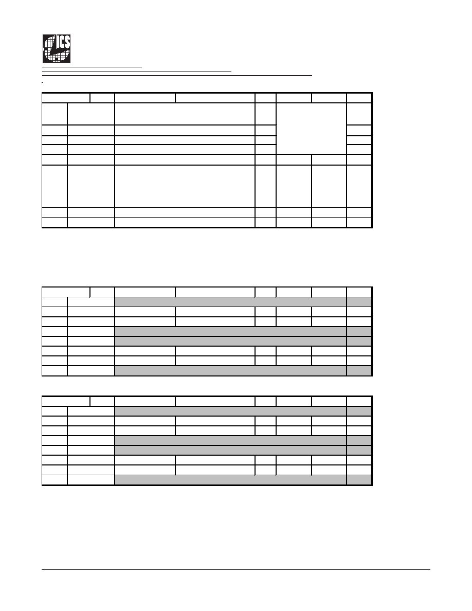
SMBus Table: Device Control Register, READ/WRITE ADDRESS (DC/DD)
Pin #
Name
Control Function
Type
0
1
PWD
Bit 7
RW
Pin 17
Bit 6
RW
Pin 6
Bit 5
RW
Pin 24
Bit 4
RW
Pin 25
Bit 3
RW
Off
On
Pin 16
Bit 2
RW
Hardware
Select
Software
Select
0
Bit 1
RW
Driven
Hi-Z
0
Bit 0
RW
Down
Center
0
Notes:
1. These bits reflect the state of the corresponding pins at power up, but may be written to
if Byte 0, bit 2 is set to '1'. FS3 is the SEL14M_25M# pin.
SMBus Table: Output Enable Register
Pin #
Name
Control Function
Type
0
1
PWD
Bit 7
1
Bit 6
DIF_3 EN
Output Enable
RW
Disable
Enable
1
Bit 5
DIF_2 EN
Output Enable
RW
Disable
Enable
1
Bit 4
1
Bit 3
1
Bit 2
DIF_1 EN
Output Enable
RW
Disable
Enable
1
Bit 1
DIF_0 EN
Output Enable
RW
Disable
Enable
1
Bit 0
1
SMBus Table: Output Stop Control Register
Pin #
Name
Control Function
Type
0
1
PWD
Bit 7
0
Bit 6
DIF_3 STOP EN Free Run/ Stop Enable RW
Free-run Stop-able
0
Bit 5
DIF_2 STOP EN Free Run/ Stop Enable RW
Free-run Stop-able
0
Bit 4
0
Bit 3
0
Bit 2
DIF_1 STOP EN Free Run/ Stop Enable RW
Free-run Stop-able
0
Bit 1
DIF_0 STOP EN Free Run/ Stop Enable RW
Free-run Stop-able
0
Bit 0
0
Reserved
Reserved
Reserved
See Frequency
Selection Table,
Page 1
SEL14M_25M#
1
(FS3)
FS2
1
FS1
1
FS0
1
-
-
-
-
-
-
-
Byte 2
-
-
-
-
-
-
Byte 1
-
-
-
DIF_STOP# drive mode
SPREAD TYPE
16
Spread Enable
1
-
Enable Software Control of Frequency,
Spread Enable (Spread Type always
Software Control)
24
25
Byte 0
17
6
Reserved
Reserved
Reserved
Reserved
Reserved

9
Integrated
Circuit
Systems, Inc.
ICS9FG104
0839D--06/02/05
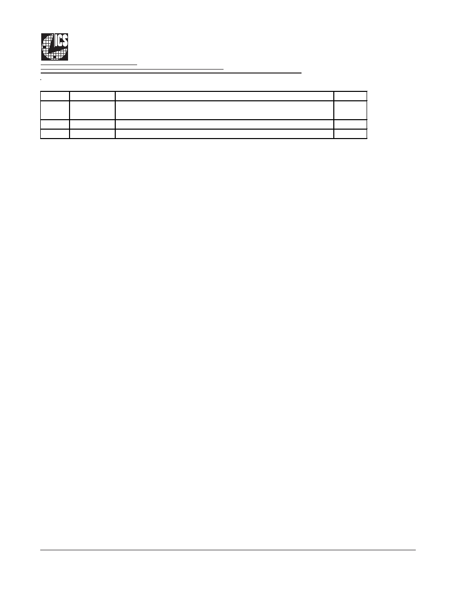
SMBus Table: Frequency Select Readback Register
Pin #
Name
Control Function
Type
0
1
PWD
Bit 7
SEL14M_25M#
1
(FS3)
State of pin 17
R
Pin 17
Bit 6
FS2
1
State of pin 6
R
Pin 6
Bit 5
FS1
1
State of pin 24
R
Pin 24
Bit 4
FS0
1
State of pin 25
R
Pin 25
Bit 3
SPREAD
1
State of pin 16
R
Off
On
Pin 16
Bit 2
0
Bit 1
0
Bit 0
0
Notes:
1. These bits reflect the state of the corresponding pins, regardless of whether software
programming is enabled or not.
SMBus Table: Vendor & Revision ID Register
Pin #
Name
Control Function
Type
0
1
PWD
Bit 7
RID3
R
-
-
X
Bit 6
RID2
R
-
-
X
Bit 5
RID1
R
-
-
X
Bit 4
RID0
R
-
-
X
Bit 3
VID3
R
-
-
0
Bit 2
VID2
R
-
-
0
Bit 1
VID1
R
-
-
0
Bit 0
VID0
R
-
-
1
SMBus Table: DEVICE ID
Pin #
Name
Control Function
Type
0
1
PWD
Bit 7
DID7
RW
-
-
0
Bit 6
DID6
RW
-
-
0
Bit 5
DID5
RW
-
-
0
Bit 4
DID4
RW
-
-
0
Bit 3
DID3
RW
-
-
1
Bit 2
DID2
RW
-
-
0
Bit 1
DID1
RW
-
-
0
Bit 0
DID0
RW
-
-
0
Byte 5
-
-
-
-
-
-
-
Byte 4
-
REVISION ID
-
-
-
-
-
16
VENDOR ID
-
-
-
25
24
See Frequency
Selection Table,
Page 1
6
17
Reserved
Reserved
Reserved
Device ID = 08 hex
Byte 3

10
Integrated
Circuit
Systems, Inc.
ICS9FG104
0839D--06/02/05
SMBus Table: Byte Count Register
Pin #
Name
Control Function
Type
0
1
PWD
Bit 7
BC7
RW
-
-
0
Bit 6
BC6
RW
-
-
0
Bit 5
BC5
RW
-
-
0
Bit 4
BC4
RW
-
-
0
Bit 3
BC3
RW
-
-
0
Bit 2
BC2
RW
-
-
1
Bit 1
BC1
RW
-
-
1
Bit 0
BC0
RW
-
-
1
SMBus Table: Reserved Register
Pin #
Name
Control Function
Type
0
1
PWD
Bit 7
0
Bit 6
0
Bit 5
0
Bit 4
0
Bit 3
0
Bit 2
0
Bit 1
0
Bit 0
0
SMBus Table: Reserved Register
Pin #
Name
Control Function
Type
0
1
PWD
Bit 7
0
Bit 6
0
Bit 5
0
Bit 4
0
Bit 3
0
Bit 2
0
Bit 1
0
Bit 0
0
SMBus Table: M/N Programming Enable
Pin #
Name
Control Function
Type
0
1
PWD
Bit 7
M/N_Enable
M/N Prog. Enable
RW
Disable
Enable
0
Bit 6
1
Bit 5
REFOUT_En
REFOUT Enable
RW
Disable
Enable
1
Bit 4
0
Bit 3
0
Bit 2
0
Bit 1
0
Bit 0
0
Reserved
Reserved
Byte 6
Reserved
Reserved
Reserved
Writing to this register
will configure how
many bytes will be
read back, default is
07
= 7 bytes.
-
-
-
-
-
-
-
-
Reserved
Reserved
Reserved
-
Reserved
Reserved
Reserved
-
-
-
-
Byte 7
-
-
-
-
-
-
-
Byte 8
-
-
-
Reserved
Reserved
Reserved
Reserved
5
-
Reserved
Reserved
Byte 9
-
-
-
Reserved
Reserved
Reserved
Reserved
-
Reserved
-
-
-

11
Integrated
Circuit
Systems, Inc.
ICS9FG104
0839D--06/02/05
SMBus Table: PLL Frequency Control Register
Pin #
Name
Control Function
Type
0
1
PWD
Bit 7
PLL N Div8
N Divider Prog bit 8
RW
X
Bit 6
PLL N Div9
N Divider Prog bit 9
RW
X
Bit 5
PLL M Div5
RW
X
Bit 4
PLL M Div4
RW
X
Bit 3
PLL M Div3
RW
X
Bit 2
PLL M Div2
RW
X
Bit 1
PLL M Div1
RW
X
Bit 0
PLL M Div0
RW
X
SMBus Table: PLL Frequency Control Register
Pin #
Name
Control Function
Type
0
1
PWD
Bit 7
PLL N Div7
RW
X
Bit 6
PLL N Div6
RW
X
Bit 5
PLL N Div5
RW
X
Bit 4
PLL N Div4
RW
X
Bit 3
PLL N Div3
RW
X
Bit 2
PLL N Div2
RW
X
Bit 1
PLL N Div1
RW
X
Bit 0
PLL N Div0
RW
X
SMBus Table: PLL Spread Spectrum Control Register
Pin #
Name
Control Function
Type
0
1
PWD
Bit 7
PLL SSP7
RW
X
Bit 6
PLL SSP6
RW
X
Bit 5
PLL SSP5
RW
X
Bit 4
PLL SSP4
RW
X
Bit 3
PLL SSP3
RW
X
Bit 2
PLL SSP2
RW
X
Bit 1
PLL SSP1
RW
X
Bit 0
PLL SSP0
RW
X
SMBus Table: PLL Spread Spectrum Control Register
Pin #
Name
Control Function
Type
0
1
PWD
Bit 7
0
Bit 6
PLL SSP14
RW
X
Bit 5
PLL SSP13
RW
X
Bit 4
PLL SSP12
RW
X
Bit 3
PLL SSP11
RW
X
Bit 2
PLL SSP10
RW
X
Bit 1
PLL SSP9
RW
X
Bit 0
PLL SSP8
RW
X
Byte 10
-
The decimal
representation of M and
N Divider in Byte 11 and
12 will configure the PLL
VCO frequency.
Default at power up =
latch-in or Byte 0 Rom
table. VCO Frequency
= 14.318 x
[NDiv(9:0)+8] /
[MDiv(5:0)+2]
-
-
M Divider
Programming
bit (5:0)
-
-
-
-
-
Byte 11
-
N Divider
Programming Byte11
bit(7:0) and Byte10
bit(7:6)
The decimal
representation of M and
N Divider in Byte 11 and
12 will configure the PLL
VCO frequency.
Default at power up =
latch-in or Byte 0 Rom
table. VCO Frequency
= 14.318 x
[NDiv(9:0)+8] /
[MDiv(5:0)+2]
-
-
-
-
-
-
-
Byte 12
-
Spread Spectrum
Programming bit(7:0)
These Spread
Spectrum bits in Byte
13 and 14 will program
the spread pecentage
of PLL
-
-
-
-
-
-
-
Byte 13
-
Reserved
Spread Spectrum
Programming bit(14:8)
These Spread
Spectrum bits in Byte
13 and 14 will program
the spread pecentage
of PLL
-
-
-
-
-
-
-

12
Integrated
Circuit
Systems, Inc.
ICS9FG104
0839D--06/02/05
Asserting DIF_STOP# pin stops all DIF outputs that are set to be stoppable after their next transition. When the SMBus
DIF_STOP tri-state bit corresponding to the DIF output of interest is programmed to a '0', DIF output will stop DIF_True =
HIGH and DIF_Complement = LOW. When the SMBus DIF_STOP tri-state bit corresponding to the DIF output of interest is
programmed to a '1', DIFoutputs will be tri-stated.
DIF_STOP# - Assertion (transition from '1' to '0')
With the de-assertion of DIF_STOP# all stopped DIF outputs will resume without a glitch. The maximum latency from the
de-assertion to active outputs is 2 - 6 DIF clock periods. If the control register tristate bit corresponding to the output of
interest is programmed to '1', then the stopped DIF outputs will be driven High within 15nS of DIF_Stop# de-assertion to a
voltage greater than 200mV.
DIF_STOP# - De-assertion (transition from '0' to '1')
DIF_STOP#
DIF
DIF#
DIF_Stop#
Tdrive_DIF_Stop, 15nS >200mV
DIF
DIF#
DIF Internal

13
Integrated
Circuit
Systems, Inc.
ICS9FG104
0839D--06/02/05
Ordering Information
ICS9FG104yFLFT
Example:
INDEX
AREA
INDEX
AREA
1 2
N
D
h x 45∞
E1
E
SEATING
PLANE
SEATING
PLANE
A1
A
e
- C -
b
.10 (.004) C
.10 (.004) C
c
L
Designation for tape and reel packaging
RoHS Compliant (Optional)
Package Type
F = SSOP
Revision Designator (will not correlate with datasheet revision)
Device Type (consists of 3 to 7 digit numbers)
Prefix
ICS, AV = Standard Device
ICS XXXX y F - LF T
MIN
MAX
MIN
MAX
A
--
2.00
--
.079
A1
0.05
--
.002
--
A2
1.65
1.85
.065
.073
b
0.22
0.38
.009
.015
c
0.09
0.25
.0035
.010
D
E
7.40
8.20
.291
.323
E1
5.00
5.60
.197
.220
e
L
0.55
0.95
.022
.037
N
0∞
8∞
0∞
8∞
VARIATIONS
MIN
MAX
MIN
MAX
28
9.90
10.50
.390
.413
(204mil) (25.6 mil)
Reference Doc.: JEDEC Publication 95, MO-150
0.0256 BASIC
COMMON DIMENSIONS
In Millimeters
In Inches
COMMON DIMENSIONS
5.3 mm. Body, 0.65 mm. Pitch SSOP
N
SEE VARIATIONS
SEE VARIATIONS
D mm.
D (inch)
SYMBOL
SEE VARIATIONS
SEE VARIATIONS
0.65 BASIC

14
Integrated
Circuit
Systems, Inc.
ICS9FG104
0839D--06/02/05
MIN
MAX
MIN
MAX
A
--
1.20
--
.047
A1
0.05
0.15
.002
.006
A2
0.80
1.05
.032
.041
b
0.19
0.30
.007
.012
c
0.09
0.20
.0035
.008
D
E
E1
4.30
4.50
.169
.177
e
L
0.45
0.75
.018
.030
N
0∞
8∞
0∞
8∞
aaa
--
0.10
--
.004
VARIATIONS
MIN
MAX
MIN
MAX
28
9.60
9.80
.378
.386
10-0035
4.40 mm. Body, 0.65 mm. Pitch TSSOP
6.40 BASIC
0.252 BASIC
0.0256 BASIC
COMMON DIMENSIONS
In Millimeters
In Inches
COMMON DIMENSIONS
(173 mil) (25.6 mil)
SYMBOL
SEE VARIATIONS
SEE VARIATIONS
0.65 BASIC
Reference Doc.: JEDEC Publication 95, MO-153
N
SEE VARIATIONS
SEE VARIATIONS
D mm.
D (inch)
INDEX
AREA
INDEX
AREA
1 2
1 2
N
D
E1
E
SEATING
PLANE
SEATING
PLANE
A1
A
A2
e
- C -
- C -
b
c
L
aaa
C
Ordering Information
ICS9FG104yGLFT
Example:
Designation for tape and reel packaging
RoHS Compliant (Optional)
Package Type
G = TSSOP
Revision Designator (will not correlate with datasheet revision)
Device Type (consists of 3 to 7 digit numbers)
Prefix
ICS, AV = Standard Device
ICS XXXX y G LF T
15
Integrated
Circuit
Systems, Inc.
ICS9FG104
0839D--06/02/05
Revision History
Rev.
Issue Date Description
Page #
D
6/2/2005
1. Updated SMBus Byte 3 bit 7, 5, 4 and 3.
2. Updated LF Ordering Information to RoHS Compliant.
9, 13-14